CS5343-DZZ中文资料
98 dB, 96 kHz, Multi-Bit Audio A/D Converter
Features
!Advanced Multi-Bit ?Σ Architecture !24-bit Conversion
!Supports Audio Sample Rates Up to 108kHz !98dB Dynamic Range at 5V !-90dB THD+N
!Low-Latency Digital Filter
!High-Pass Filter to Remove DC Offsets !Single +3.3 V or +5 V Power Supply !Power Consumption Less Than 50 mW !Master or Slave Operation !Slave Mode Speed Auto-Detect !Master Mode Default Settings !256x or 384x MCLK/LRCK Ratio !CS5343 Supports I2S Audio Format
!CS5344 Supports Left-Justified Audio Format
General Description
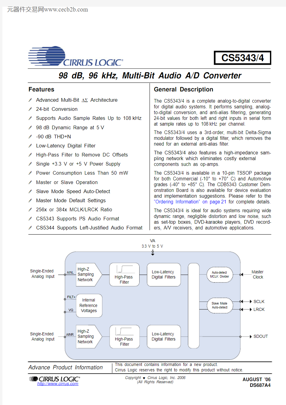
The CS5343/4 is a complete analog-to-digital converter for digital audio systems. It performs sampling, analog-to-digital conversion, and anti-alias filtering, generating 24-bit values for both left and right inputs in serial form at sample rates up to 108kHz per channel.
The CS5343/4 uses a 3rd-order, multi-bit Delta-Sigma modulator followed by a digital filter, which removes the need for an external anti-alias filter.
The CS5343/4 also features a high-impedance sam-pling network which eliminates costly external components such as op-amps.
The CS5343/4 is available in a 10-pin TSSOP package for both Commercial (-10° to +70° C) and Automotive grades (-40° to +85° C). The CDB5343 Customer Dem-onstration Board is also available for device evaluation and implementation suggestions. Please refer to the “Ordering Information” on page 21 for complete details.The CS5343/4 is ideal for audio systems requiring wide dynamic range, negligible distortion and low noise, such as set-top boxes, DVD-karaoke players, DVD record-ers, A/V receivers, and automotive applications.
CS5343/4
CS5343/4 TABLE OF CONTENTS
1. PIN DESCRIPTIONS (4)
2. CHARACTERISTICS AND SPECIFICATIONS (5)
SPECIFIED OPERATING CONDITIONS (5)
ABSOLUTE MAXIMUM RATINGS (5)
ANALOG CHARACTERISTICS - COMMERCIAL GRADE (6)
ANALOG CHARACTERISTICS - AUTOMOTIVE GRADE (7)
DIGITAL FILTER CHARACTERISTICS (8)
DC ELECTRICAL CHARACTERISTICS (8)
DIGITAL CHARACTERISTICS (9)
SYSTEM CLOCKING AND SERIAL AUDIO INTERFACE (10)
3. TYPICAL CONNECTION DIAGRAM (12)
4. APPLICATIONS (13)
4.1 Operation as Clock Master or Slave (13)
4.1.1 Slave Mode Operation (13)
4.1.2 Master Mode Operation (14)
4.1.2.1 Master Mode Speed Selection (14)
4.1.3 Master Clock (14)
4.2 Serial Audio Interface (15)
4.3 Digital Interface (15)
4.4 Analog Connections (15)
4.4.1 Component Values (16)
4.5 Grounding and Power Supply Decoupling (16)
4.6 Synchronization of Multiple Devices (17)
5. FILTER PLOTS (17)
6. PARAMETER DEFINITIONS (19)
7. PACKAGE DIMENSIONS (20)
THERMAL CHARACTERISTICS (20)
8. ORDERING INFORMATION (21)
9. REVISION HISTORY (21)
LIST OF FIGURES
Figure 1. CS5343 I2S Serial Audio Interface (11)
Figure 2. CS5344 Left-Justified Serial Audio Interface (11)
Figure 3. Typical Connection Diagram (12)
Figure 4. I2S Serial Audio Interface (15)
Figure 5. Left-Justified Serial Audio Interface (15)
Figure 6. CS5343/4 Analog Input Network (15)
Figure 7. CS5343/4 Example Analog Input Network (16)
Figure 8. Single-Speed Mode Stopband Rejection (17)
Figure 9. Single-Speed Mode Transition Band (17)
Figure 10. Single-Speed Mode Transition Band (Detail) (17)
Figure 11. Single-Speed Mode Passband Ripple (17)
Figure 12. Double-Speed Mode Stopband Rejection (18)
Figure 13. Double-Speed Mode Transition Band (18)
Figure 14. Double-Speed Mode Transition Band (Detail) (18)
Figure 15. Double-Speed Mode Passband Ripple (18)
CS5343/4 LIST OF TABLES
Table 1. Master/Slave Mode Selection (13)
Table 2. Speed Modes and the Associated Sample Rates (Fs) in Slave Mode (13)
Table 3. Speed Modes and the Associated Sample Rates (Fs) in Master Mode (14)
Table 4. Speed Mode Selection in Master Mode (14)
Table 5. Common MCLK Frequencies in Master and Slave Modes (14)
Table 6. Analog Input Design Parameters (16)
CS5343/4
1.PIN DESCRIPTIONS
Pin Name Pin #
Pin Description
SDOUT 1Serial Audio Data Output (Output ) - Output for two’s complement serial audio data. Also selects Master or Slave Mode.
SCLK 2Serial Clock (Input/Output ) - Serial clock for the serial audio interface.
LRCK 3Left Right Clock (Input/Output ) - Determines which channel, Left or Right, is currently active on the serial audio data line.
MCLK 4Master Clock (Input ) - Clock source for the delta-sigma modulator and digital filters.
FILT+5Positive Voltage Reference (Output ) - Positive reference voltage for the internal sampling circuits.AINL AINR 68Analog Input (Input ) - The full-scale analog input level is specified in the Analog Characteristics specifi-cation table.
VQ 7Quiescent Voltage (Output) - Filter connection for the internal quiescent reference voltage.GND 9Ground (Input ) - Ground reference. Must be connected to analog ground.VA
10
Power (Input ) - Positive power supply for the digital and analog sections.
SDOUT SCLK MCLK FILT+
VA GND AINR VQ AINL
CS5343/4
2.CHARACTERISTICS AND SPECIFICATIONS
(All Min/Max characteristics and specifications are guaranteed over the Specified Operating Conditions . Typical performance characteristics and specifications are derived from measurements taken at typical supply voltages and T A = 25°C.)
SPECIFIED OPERATING CONDITIONS
(GND = 0V, all voltages with respect to GND.)
ABSOLUTE MAXIMUM RATINGS
(GND = 0 V, all voltages with respect to GND.) (Note 1)
Notes:
1.Operation beyond these limits may result in permanent damage to the device. Normal operation is not
guaranteed at these extremes.2.Any pin except supplies. Transient currents of up to ±100mA on the analog input pins will not cause
SCR latch-up.3.The maximum over/under voltage is limited by the input current.
Parameter
Symbol Min Typ
Max
Unit
Power Supplies
VA 3.14.75 3.35.0 3.55.25V V Ambient Operating Temperature
Commercial Automotive
T AC T AD
-10-40
--
7085
°C °C
Parameter
Symbol
Min
Max
Unit
DC Power Supplies VA -0.3+6.0V Input Current (Note 2)I in -10+10mA Input Voltage
(Note 3)
V IN -0.7VA+0.7V Ambient Operating Temperature (Power Applied)T A -50+115°C Storage Temperature
T stg
-65
+150
°C
CS5343/4
ANALOG CHARACTERISTICS - COMMERCIAL GRADE
Test conditions (unless otherwise specified): Input test signal is a 1 kHz sine wave; measurement bandwidth is 10Hz to 20kHz; source impedance less than or equal to 2.5 k ?.Notes:
4.Referred to the typical full-scale input voltage
Dynamic Performance for Commercial Grade
VA = 3.3V
VA = 5.0V
Single-Speed Mode Fs = 48 kHz Symbol
Min Typ Max Min Typ Max Unit Dynamic Range
A-weighted unweighted 89869592--92899895--dB dB Total Harmonic Distortion + Noise
(Note 4) -1dB -20dB -60dB THD+N ----86-75-35-80------90-78-38-84--dB dB dB Double-Speed Mode Fs = 96kHz Min Typ Max Min Typ Max Unit Dynamic Range
A-weighted unweighted
89869592--92899895--dB dB Total Harmonic Distortion + Noise
(Note 4) -1dB -20dB -60dB
THD+N ----86-75-35
-80-----
-90-78-38
-84--dB dB dB Dynamic Performance for Commercial Grade - All Modes
Min
Typ Max Unit Interchannel Isolation
-90-dB DC Accuracy
Interchannel Gain Mismatch --0.1dB Gain Error -3-+3%Gain Drift
-±100
-ppm/°C Analog Input Characteristics
Full-scale Input Voltage 0.51*VA
0.56*VA 0.57*VA
Vpp Input Impedance
-
7.5
-M ?
CS5343/4
ANALOG CHARACTERISTICS - AUTOMOTIVE GRADE
Test conditions (unless otherwise specified): Input test signal is a 1 kHz sine wave; measurement bandwidth is 10Hz to 20kHz; source impedance less than or equal to 2.5 k ?.Notes:
5.Referred to the typical full-scale input voltage
Dynamic Performance for Automotive Grade
VA = 3.3V
VA = 5.0V
Single-Speed Mode Fs = 48kHz Symbol
Min Typ Max Min Typ Max Unit Dynamic Range
A-weighted unweighted 87849592--90879895--dB dB Total Harmonic Distortion + Noise
(Note 5) -1dB -20dB -60dB THD+N ----86-75-35-78------90-78-38-82--dB dB dB Double-Speed Mode Fs = 96kHz Min Typ Max Min Typ Max Unit Dynamic Range
A-weighted unweighted
87849592--90879895--dB dB Total Harmonic Distortion + Noise
(Note 5) -1dB -20dB -60dB
THD+N ----86-75-35
-78-----
-90-78-38
-82--dB dB dB Dynamic Performance for Automotive Grade - All Modes
Min
Typ Max Unit Interchannel Isolation
-90-dB DC Accuracy
Interchannel Gain Mismatch --0.1dB Gain Error -3-+3%Gain Drift
-±100
-ppm/°C Analog Input Characteristics
Full-scale Input Voltage 0.51*VA
0.56*VA 0.57*VA
Vpp Input Impedance
-
7.5
-M ?
CS5343/4
DIGITAL FILTER CHARACTERISTICS
Notes:
6.Response shown is for Fs equal to 48 kHz. Filter characteristics scale with Fs.
DC ELECTRICAL CHARACTERISTICS
(GND = 0V, all voltages with respect to 0V. MCLK=12.288MHz; Master Mode)
Notes:
7.Device enters power-down mode when MCLK is held static.
8.Valid with the recommended capacitor values on FILT+ and VQ as shown in the Typical Connection
Diagram.
Parameter
Symbol Min Typ Max Unit
Single-Speed Mode Fs = 4 - 54kHz
Passband (-0.1 dB)
0-0.489Fs Passband Ripple -0.025-0.025dB Stopband
0.560--Fs Stopband Attenuation
69--dB Total Group Delay (Fs = Output Sample Rate)
t gd
-12/Fs -s Double-Speed Mode Fs = 86 - 108kHz
Passband (-0.1 dB)
0-0.489Fs Passband Ripple -0.025-0.025dB Stopband
0.560--Fs Stopband Attenuation
69
--dB Total Group Delay (Fs = Output Sample Rate)
t gd
-9/Fs -s High-Pass Filter Characteristics
Frequency Response -3.0 dB -0.13 dB (Note 6)-120--Hz Hz Phase Deviation @ 20Hz
(Note 6)
-10-Deg Passband Ripple
--0
dB
Parameter
Symbol VA = 3.3 V
VA = 5.0 V Min
Typ
Max Min
Typ
Max
Unit
DC Power Supplies:
VA 3.1 3.3--5 5.25V Power Supply Current (Normal Operation)I A -15--15-mA Power Supply Current (Power-Down Mode) (Note 7)I A - 1.1-- 1.1-mA Power Consumption
(Normal Operation)
(Power-Down Mode) (Note 7)
----503.6
----
755.5
--mW mW
Parameter
Symbol
Min Typ
Max Unit
Power Supply Rejection Ratio (1kHz)(Note 8)
PSRR
-65-dB V Q Nominal Voltage Output Impedance
--0.44xVA 25--V k ?Filt+ Nominal Voltage Output Impedance
Maximum allowable DC current source/sink
---
VA 2202.5
---
V k ?uA
CS5343/4 DIGITAL CHARACTERISTICS
Parameter Symbol Min Typ Max Units High-Level Input Voltage (% of VA)V IH70--% Low-Level Input Voltage(% of VA)V IL--30% High-Level Output Voltage at I o = 500μA(%of VA)V OH70--% Low-Level Output Voltage at I o =500μA(%of VA)V OL--15% Input Leakage Current I in-10-10μA
CS5343/4
SYSTEM CLOCKING AND SERIAL AUDIO INTERFACE
(Logic “0” = GND = 0V; Logic “1” = VA, C L = 20pF) Parameter
Symbol Min Typ Max Unit
Master Mode
MCLK Period
(Double-Speed, 384x Mode)t clkw
24-30ns (Double-Speed, 192x Mode)48-60ns (Double-Speed, 256x Mode)36-45ns (Double-Speed, 128x Mode)72-90ns (Single-Speed, 768x Mode)24-325ns (Single-Speed, 384x Mode)48-651ns (Single-Speed, 512x Mode)36-488ns (Single-Speed, 256x Mode)
72-976ns MCLK Duty Cycle 405060%Output Sample Rate (Single-Speed)(Double-Speed)
Fs 486--54
108kHz kHz LRCK Duty Cycle -50-%SCLK Duty Cycle
-50-%SDOUT valid before SCLK rising t stp 10--ns SDOUT valid after SCLK rising t hld 40--ns SCLK falling to LRCK edge
t slrd
-20-20ns Slave Mode
MCLK Period
(Double-Speed, 384x Mode)t clkw
24-30ns (Double-Speed, 192x Mode)48-60ns (Double-Speed, 256x Mode)36-45ns (Double-Speed, 128x Mode)72-90ns (Single-Speed, 768x Mode)24-325ns (Single-Speed, 384x Mode)48-651ns (Single-Speed, 512x Mode)36-488ns (Single-Speed, 256x Mode)
72-976ns MCLK Duty Cycle 405060%Input Sample Rate (Single-Speed)
(Double-Speed)
Fs 486--54108kHz kHz LRCK Duty
Cycle 405060%SCLK Period t sclkw
--ns SCLK Duty
Cycle
455055%SDOUT valid before SCLK rising t stp 10--ns SDOUT valid after SCLK rising t hld 10--ns SCLK falling to LRCK edge
t slrd -20
-20
ns
164Fs ×------------------
CS5343/4 Array
Figure 1. CS5343 I2S Serial Audio Interface
Figure 2. CS5344 Left-Justified Serial Audio Interface
CS5343/4
3.TYPICAL CONNECTION DIAGRAM
Figure 3. Typical Connection Diagram
in the “Master Mode Speed Selection” section on page 14
CS5343/4
4.APPLICATIONS
4.1
Operation as Clock Master or Slave
The CS5343/4 supports operation as either a clock master or slave. As a clock master, the left/right and serial clocks are synchronously generated on-chip and output on the LRCK and SCLK pins, respectively.As a clock slave, the LRCK and SCLK pins are always inputs and require external generation of the left/right and serial clocks. The selection of clock master or slave is made via a 10 k ? pull-up resistor from SDOUT to VA for Master Mode selection or via a 10 k ? pull-down resistor from SDOUT to GND for Slave Mode se-lection, as shown in Table 1.
4.1.1Slave Mode Operation
A unique feature of the CS5343/4 is the automatic selection of either Single- or Double-Speed Mode when acting as a clock slave. The auto-mode selection feature supports all standard audio sample rates from 4 to 108kHz. Please refer to Table 2 for supported sample rate ranges in Slave Mode.
Table 2. Speed Modes and the Associated Sample Rates (Fs) in Slave Mode
Mode
Selection
Master Mode 10 k ? pull-up resistor from SDOUT to VA Slave Mode
10 k ? pull-down resistor from SDOUT to GND
Table 1. Master/Slave Mode Selection
Speed Mode
MCLK/LRCK
Ratio
SCLK/LRCK
Ratio
Input Sample Rate Range (kHz)
Single-Speed Mode
256x
64 4 - 54512x 64 4 - 54384x 48, 64 4 - 54768x 48, 64 4 - 54Double-Speed Mode
128x
6486 - 108256x 6486 - 108192x 48, 6486 - 108384x
48, 64
86 - 108
CS5343/4
4.1.2
Master Mode Operation
As clock Master, the CS5343/4 generates LRCK and SCLK synchronously on-chip. Table 3 shows the available sample rates and associated clock ratios in Master Mode.
4.1.2.1Master Mode Speed Selection
During power-up in Master Mode, the LRCK and SCLK pins are inputs to configure speed mode and the output clock ratio. The LRCK pin is pulled low internally to select Single-Speed Mode by default, but Dou-ble-Speed Mode is accessed with a 10 k ? pull-up resistor from LRCK to VA as shown in Table 4. Simi-larly, the SCLK pin is internally pulled-low by default to select a 256x MCLK/LRCK ratio, but a MCLK/LRCK ratio of 348x is accessed with a 10 k ? pull-up resistor from SCLK to VA as shown in Table 4.Following the power-up routine, the LRCK and SCLK pins become clock outputs.
4.1.3Master Clock
The CS5343/4 requires a Master clock (MCLK) which runs the internal sampling circuits and digital filters.There is also an internal MCLK divider which is automatically activated based on the frequency of the MCLK. Table 4 lists some common audio output sample rates and the required MCLK frequency.
Speed Mode
MCLK/LRCK
Ratio
SCLK/LRCK
Ratio
Input Sample Rate Range (kHz)
Single-Speed Mode
256x
64 4 - 54512x 64 4 - 54384x 64 4 - 54768x 64 4 - 54Double-Speed Mode
128x
6486 - 108256x 6486 - 108192x 6486 - 108384x
64
86 - 108
Table 3. Speed Modes and the Associated Sample Rates (Fs) in Master Mode
Pin
Resistor Option
Clock Configuration
LRCK Internal Pull-Down to GND (100 k ?)Single-Speed Mode (default)
External Pull-Up to VA (10 k ?)Double-Speed Mode SCLK
Internal Pull-Down to GND (100 k ?)256x MCLK/LRCK (default)
External Pull-Up to VA (10 k ?)
384x MCLK/LRCK
Table 4. Speed Mode Selection in Master Mode
Master and Slave Mode
Sample Rate (kHz)
Speed Mode
MCLK(MHz)
MCLK (MHz)
256x 512x 384x 768x 32SSM 8.91216.38412.28824.57644.1SSM 11.28922.57916.93433.86848
SSM
12.288
24.57618.43236.864Sample Rate (kHz)
Speed Mode
MCLK(MHz)
MCLK (MHz)
128x 256x 192x 384x 88.2DSM 11.28922.57916.93433.86896
DSM
12.288
24.576
18.432
36.864
Table 5. Common MCLK Frequencies in Master and Slave Modes
CS5343/4
4.2
Serial Audio Interface
The CS5343 output is serial data in I2S audio format and the CS5344 output is serial data in Left-Justified audio format. Figures 4 and 5 show the I2S and Left-Justified data relative to SCLK and LRCK. Additionally,Figures 1 and 2 display more information on the required timing for the serial audio interface format. For an overview of serial audio interface formats, please refer to Cirrus Application Note AN282.
4.3Digital Interface
VA supplies power to both the analog and digital sections of the ADC, and also powers the serial port. Con-sequently, the digital interface logic level must equal VA to within the limits specified under “Digital Charac-teristics” on page 9.
4.4Analog Connections
The analog modulator samples the input signal at half of the internal master clock rate, or 6.144MHz when MCLK = 12.288 MHz. The digital filter will reject signals within the stopband of the filter. However, there is no rejection for input signals which are multiples of the input sampling frequency (n ×6.144MHz), where n=0,1,2,... Refer to Figure 6 which shows the recommended topology of the analog input network. The ex-ternal shunt capacitor and internal input impedance form a single-pole RC filter to provide the appropriate filtering of noise at the modulator sampling frequency. Additionally, the 180 pF capacitor acts as a charge source for the internal sampling circuits. Capacitors of NPO or other high-quality dielectric will produce the best results while capacitors with a large voltage coefficient (such as general-purpose ceramics) can de-grade signal linearity.
Figure 4. I2S Serial Audio Interface
Figure 5. Left-Justified Serial Audio Interface
Figure 6. CS5343/4 Analog Input Network
CS5343/4
4.4.1
Component Values
Three parameters determine the values of resistors R1 and R2 as shown in Figure 6: source impedance,attenuation, and input impedance. Table 6 shows the design equation used to determine these values.?
Source Impedance: Source impedance is defined as the impedance as seen from the ADC looking back into the signal network. The ADC achieves optimal THD+N performance with a source imped-ance less than or equal to 2.5 k ?.
?
Attenuation: The required attenuation factor depends on the magnitude of the input signal. The full-scale input voltage is specified under “Analog Characteristics - Commercial Grade” on page 6. The user should select values for R1 and R2 such that the magnitude of the incoming signal multiplied by the attenuation factor is less than or equal to the full-scale input voltage of the device.
?
Input Impedance: Input impedance is the impedance from the signal source to the ADC analog input pins. Table 6 shows the input parameters and the associated design equations.
Figure 7 illustrates an example configuration using two 4.99 k ? resistors in place of R1 and R2. Based on the discussion above, this circuit provides an optimal interface for both the ADC and the signal source.First, consumer equipment frequently requires an input impedance of 10 k ?, which the 4.99 k ? resistors provide. Second, this circuit will attenuate a typical line level voltage, 2 Vrms, to the full-scale input of the ADC, 1 Vrms when VA = 5 V. Finally, at 2.5 k ?, the source impedance optimizes analog performance of the ADC.
4.5Grounding and Power Supply Decoupling
As with any high-resolution converter, designing with the CS5343/4 requires careful attention to power sup-ply and grounding arrangements if its potential performance is to be realized. Figure 3 shows the recom-mended power arrangements, with VA connected to a clean supply. Decoupling capacitors should be as near to the ADC as possible, with the low value ceramic capacitor being the nearest. All signals, especially clocks, should be kept away from the FILT+ and VQ pins in order to avoid unwanted coupling into the mod-ulators. The FILT+ and VQ decoupling capacitors, particularly the 0.01μF, must be positioned to minimize the electrical path from FILT+ to GND. The CDB5343 evaluation board demonstrates the optimum layout and power supply arrangements. To minimize digital noise, connect the ADC digital outputs only to CMOS inputs.
Source Impedance
Attenuation Factor
Input Impedance
Table 6. Analog Input Design Parameters
R 1R 2×()R 1R 2+------------------------R 2()R 1R 2+()------------------------R 1R 2+()
Figure 7. CS5343/4 Example Analog Input Network
CS5343/4
4.6
Synchronization of Multiple Devices
In systems where multiple ADCs are required, care must be taken to achieve simultaneous sampling. To ensure synchronous sampling, the MCLK, SCLK, and LRCK must be the same for all of the CS5343 and CS5344 devices in the system.
5.FILTER PLOTS
Figure 8. Single-Speed Mode Stopband Rejection
Figure 9. Single-Speed Mode Transition Band
Figure 10. Single-Speed Mode Transition Band (Detail)
Figure 11. Single-Speed Mode Passband Ripple
CS5343/4
Figure 12. Double-Speed Mode Stopband Rejection
Figure 13. Double-Speed Mode Transition Band
Figure 14. Double-Speed Mode Transition Band (Detail)Figure 15. Double-Speed Mode Passband Ripple
CS5343/4 6.PARAMETER DEFINITIONS
Dynamic Range
The ratio of the rms value of the signal to the rms sum of all other spectral components over the specified bandwidth. Dynamic Range is a signal-to-noise ratio measurement over the specified bandwidth made with
a -60dBFS signal. 60dB is added to resulting measurement to refer the measurement to full-scale. This
technique ensures that the distortion components are below the noise level and do not affect the measure-ment. This measurement technique has been accepted by the Audio Engineering Society, AES17-1991, and the Electronic Industries Association of Japan, EIAJ CP-307. Expressed in decibels.
Total Harmonic Distortion + Noise
The ratio of the rms value of the signal to the rms sum of all other spectral components over the specified bandwidth (typically 10Hz to 20kHz), including distortion components. Expressed in decibels. Measured at -1 and -20dBFS as suggested in AES17-1991 Annex A.
Frequency Response
A measure of the amplitude response variation from 10Hz to 20kHz relative to the amplitude response at
1kHz. Units in decibels.
Interchannel Isolation
A measure of crosstalk between the left and right channels. Measured for each channel at the converter's
output with no signal to the input under test and a full-scale signal applied to the other channel. Units in deci-bels.
Interchannel Gain Mismatch
The gain difference between left and right channels. Units in decibels.
Gain Error
The deviation from the nominal full-scale analog input for a full-scale digital output.
Gain Drift
The change in gain value with temperature. Units in ppm/°C.
Offset Error
The deviation of the mid-scale transition (111...111 to 000...000) from the ideal. Units in mV.
CS5343/4
7.PACKAGE DIMENSIONS
Notes:
1.Reference document: JEDEC MO-187
2. D does not include mold flash or protrusions which is 0.15 mm max. per side.
3.E1 does not include inter-lead flash or protrusions which is 0.15 mm max per side.
4.Dimension b does not include a total allowable dambar protrusion of 0.08 mm max.
5.Exceptions to JEDEC dimension.
THERMAL CHARACTERISTICS
INCHES
MILLIMETERS
NOTE
DIM
MIN
NOM
MAX
MIN
NOM
MAX
A ----0.0433---- 1.10A10--0.00590
--0.15A20.0295--0.03740.75
--0.95b 0.0059--0.01180.15
--0.304, 5c 0.0031--0.00910.08
--0.23D --0.1181 BSC ---- 3.00 BSC --2E --0.1929 BSC ---- 4.90 BSC --E1--0.1181 BSC ---- 3.00 BSC --3
e --0.0197 BSC ----0.50 BSC --L 0.01570.02360.03150.400.600.80L1--0.0374 REF ----0.95 REF
--μ
0°
--8°0°
--
8°
Controlling Dimension is Millimeters
Parameter
Symbol
Min
Typ
Max
Unit Allowable Junction Temperature T J
--135°C Junction to Ambient Thermal Impedance
(4-layer PCB)(2-layer PCB)
θJA-4θJA-2
--
100170
--
°C/W °C/W
10LD TSSOP (3mm BODY) PACKAGE DRAWING (Note 1)
E
N
123
e
b A1
A2A
D
SEATING PLANE E11
L SIDE VIEW
END VIEW
TOP VIEW
∝
L1
c