IRF740S中文资料
IRF740S
N -CHANNEL 400V -0.48?-10A -D 2
PAK
PowerMESH ?MOSFET
s TYPICAL R DS(on)=0.48?
s EXTREMELY HIGH dv/dt CAPABILITY s 100%AVALANCHE TESTED
s VERY LOW INTRINSIC CAPACITANCES s GATE CHARGE MINIMIZED
s
FOR THROUGH-HOLE VERSION CONTACT SALES OFFICE
DESCRIPTION
This power MOSFET is designed using the company’s consolidated strip layout-based MESH OVERLAY ?process.This technology matches and improves the performances compared with standard parts from various sources.
APPLICATIONS s HIGH CURRENT SWITCHING s UNINTERRUPTIBLE POWER SUPPLY (UPS)s DC/DC COVERTERS FOR TELECOM,
INDUSTRIAL,AND LIGHTING EQUIPMENT.
?
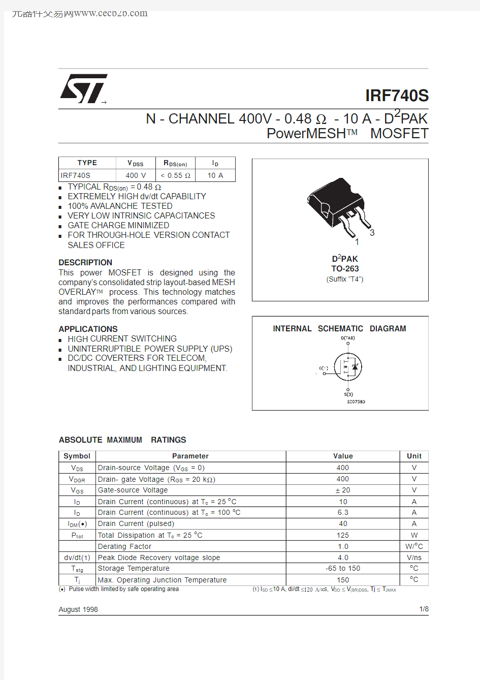
INTERNAL SCHEMATIC DIAGRAM
August 1998ABSOLUTE MAXIMUM RATINGS
Symbol Parameter
Value Unit V DS Drain-source Voltage (V GS =0)400V V DGR Drain-gate Voltage (R GS =20k ?)400V V GS Gate-source Voltage
±20V I D Drain Current (continuous)at T c =25o
C 10A I
D Drain Current (continuous)at T c =100o C 6.3A I DM (?)Drain Current (pulsed)
40A P t ot Total Dissipation at T c =25o
C 125W Derating Factor
1.0W/o
C dv/dt(1)Peak Diode Recovery voltage slope 4.0V/ns
T stg Storage Temperature
-65to 150
o C T j
Max.Operating Junction Temperature
150
o C
(?)Pulse width limited by safe operating area
(1)I SD ≤10A,di/dt ≤120 Α/μs,V DD ≤V (BR)DSS ,Tj ≤T JMAX
TYPE V DSS R DS(on)I D IRF740S
400V
<0.55?
10A
1
3
D 2PAK TO-263
(Suffix ”T4”)
1/8
THERMAL DATA
R t hj-ca se Rthj-amb R thc-si nk
T l Thermal Resistance Junction-case Max
Thermal Resistance Junction-ambient Max
Thermal Resistance Case-sink Typ
Maximum Lead Temperature For Soldering Purpose
1.0
62.5
0.5
300
o C/W
oC/W
o C/W
o C
AVALANCHE CHARACTERISTICS
Symbol Parameter Max Value Unit
I AR Avalanche Current,Repetitive or Not-Repetitive
(pulse width limited by T j max)
10A
E AS Single Pulse Avalanche Energy
(starting T j=25o C,I D=I AR,V DD=50V)
520mJ
ELECTRICAL CHARACTERISTICS(T case=25o C unless otherwise specified)
OFF
Symbol Parameter Test Conditions Min.Typ.Max.Unit V(BR)DSS Drain-source
Breakdown Voltage
I D=250μA V GS=0400V
I DSS Zero Gate Voltage
Drain Current(V GS=0)V DS=Max Rating
V DS=Max Rating T c=125o C
1
50
μA
μA
I GSS Gate-body Leakage
Current(V DS=0)
V GS=±20V±100nA ON(?)
Symbol Parameter Test Conditions Min.Typ.Max.Unit V GS(th)Gate Threshold
Voltage
V DS=V GS I D=250μA234V
R DS(on)Static Drain-source On
Resistance
V GS=10V I D=5.3A0.480.55?
I D(o n)On State Drain Current V DS>I D(on)x R DS(on)max
V GS=10V
10A DYNAMIC
Symbol Parameter Test Conditions Min.Typ.Max.Unit
g fs(?)Forward
Transconductance
V DS>I D(on)x R DS(on)max I D=6A 5.8S
C iss C oss C rss Input Capacitance
Output Capacitance
Reverse Transfer
Capacitance
V DS=25V f=1MHz V GS=01400
220
27
pF
pF
pF
IRF740S 2/8
ELECTRICAL CHARACTERISTICS(continued)
SWITCHING ON
Symbol Parameter Test Conditions Min.Typ.Max.Unit
t d(on) t r Turn-on Time
Rise Time
V DD=200V I D=5A
R G=4.7 ?V GS=10V
(see test circuit,figure1)
17
10
ns
ns
Q g Q gs Q gd Total Gate Charge
Gate-Source Charge
Gate-Drain Charge
V DD=320V I D=10.7A V GS=10V35
11
12
43nC
nC
nC
SWITCHING OFF
Symbol Parameter Test Conditions Min.Typ.Max.Unit
t r(Vof f) t f
t c Off-voltage Rise Time
Fall Time
Cross-over Time
V DD=320V I D=10A
R G=4.7 ?V GS=10V
(see test circuit,figure3)
10
10
17
ns
ns
ns
SOURCE DRAIN DIODE
Symbol Parameter Test Conditions Min.Typ.Max.Unit
I SD I SDM(?)Source-drain Current
Source-drain Current
(pulsed)
10
40
A
A
V SD(?)Forward On Voltage I SD=10A V GS=0 1.6V
t rr Q rr I RRM Reverse Recovery
Time
Reverse Recovery
Charge
Reverse Recovery
Current
I SD=10A di/dt=100A/μs
V DD=100V T j=150o C
(see test circuit,figure3)
370
3.2
17
ns
μC
A
(?)Pulsed:Pulse duration=300μs,duty cycle1.5%
(?)Pulse width limited by safe operating area
Safe Operating Area Thermal Impedance
IRF740S
3/8
Output Characteristics Transconductance
Gate Charge vs Gate-source Voltage Transfer Characteristics
Static Drain-source On Resistance Capacitance Variations
IRF740S 4/8
Normalized Gate Threshold Voltage vs Temperature
Source-drain Diode Forward Characteristics Normalized On Resistance vs Temperature
IRF740S
5/8
Fig.1:Unclamped Inductive Load Test Circuit Fig.3:Switching Times Test Circuits For Resistive Load Fig.1:Unclamped Inductive Waveform Fig.4:Gate Charge test Circuit
Fig.5:Test Circuit For Inductive Load Switching And Diode Recovery Times
IRF740S
6/8
DIM.
mm
inch MIN.
TYP.
MAX.MIN.TYP.
MAX.A 4.3 4.60.1690.181A1 2.49 2.690.0980.106B 0.70.930.0270.036B2 1.25 1.40.0490.055C 0.450.60.0170.023C2 1.21 1.360.0470.053D 8.959.350.3520.368E 1010.280.3930.404G 4.88 5.280.1920.208L 1515.850.5900.624L2 1.27 1.40.0500.055L3
1.4
1.75
0.055
0.068
L2
L3
L
B2B
G
E
A
C2
D
C
A1
P011P6/C
TO-263(D 2PAK)MECHANICAL DATA
IRF740S
7/8
Information furnished is believed to be accurate and reliable.However,STMicroelectronics assumes no responsibility for the consequences of use of such information nor for any infringement of patents or other rights of third parties which may result from its use.No license is granted by implication or otherwise under any patent or patent rights of STMicroelectronics.Specification mentioned in this publication are subject to change without notice.This publication supersedes and replaces all information previously supplied.STMicroelectronics products are not authorized for use as critical components in life support devices or systems without express written approval of STMicroelectronics.
The ST logo is a registered trademark of STMicroelectronics ?1998STMicroelectronics –Printed in Italy –All Rights Reserved
STMicroelectronics GROUP OF COMPANIES
Australia -Brazil -Canada -China -France -Germany -Italy -Japan -Korea -Malaysia -Malta -Mexico -Morocco -The Netherlands -Singapore -Spain -Sweden -Switzerland -Taiwan -Thailand -United Kingdom -U.S.A.
.
IRF740S
8/8