MAX4444中文资料
Ultra-High-Speed, Low-Distortion, Differential-to-Single-Ended Line Receivers with Enable
For free samples & the latest literature: https://www.360docs.net/doc/fc1415459.html,, or phone 1-800-998-8800.For small orders, phone 1-800-835-8769.
General Description
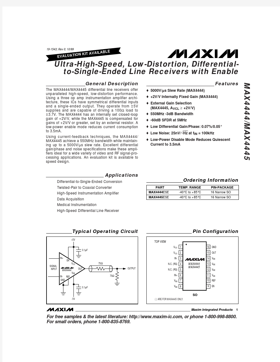
The MAX4444/MAX4445 differential line receivers offer unparalleled high-speed, low-distortion https://www.360docs.net/doc/fc1415459.html,ing a three op amp instrumentation amplifier archi-tecture, these ICs have symmetrical differential inputs and a single-ended output. They operate from ±5V supplies and are capable of driving a 100?load to ±3.7V. The MAX4444 has an internally set closed-loop gain of +2V/V, while the MAX4445 is compensated for gains of +2V/V or greater, set by an external resistor. A low-power enable mode reduces current consumption to 3.5mA.
Using current-feedback techniques, the MAX4444/MAX4445 achieve a 550MHz bandwidth while maintain-ing up to a 5000V/μs slew rate. Excellent differential gain/phase and noise specifications make these ampli-fiers ideal for a wide variety of video and RF signal-pro-cessing applications. An evaluation kit is available to speed design.
Applications
Differential-to-Single-Ended Conversion Twisted-Pair to Coaxial Converter High-Speed Instrumentation Amplifier Data Acquisition Medical Instrumentation
High-Speed Differential Line Receiver
Features
o 5000V/μs Slew Rate (MAX4444)o +2V/V Internally Fixed Gain (MAX4444)o External Gain Selection (MAX4445, A VCL
≥+2V/V)o 550MHz -3dB Bandwidth o -60dB SFDR at 5MHz
o Low Differential Gain/Phase: 0.07%/0.05°o Low Noise: 25nV/√Hz at f IN = 100kHz
o Low-Power Disable Mode Reduces Quiescent Current to 3.5mA
MAX4444/MAX4445
________________________________________________________________Maxim Integrated Products 1
Typical Operating Circuit
19-1543; Rev 0; 10/99
E V A L U A T IO
N K IT A
V A IL A B L E
Pin Configuration
Ordering Information
M A X 4444/M A X 4445
Ultra-High-Speed, Low-Distortion, Differential-to-Single-Ended Line Receivers with Enable 2_______________________________________________________________________________________
ABSOLUTE MAXIMUM RATINGS
DC ELECTRICAL CHARACTERISTICS
(V CC = +5V, V EE = -5V, V EN = ≥2V, V CM = 0 , R L = ∞, REF = GND, A VCL = +2V/V, T A = T MIN to T MAX , unless otherwise noted. Typical values are at T A = +25°C.)
Stresses beyond those listed under “Absolute Maximum Ratings” may cause permanent damage to the device. These are stress ratings only, and functional operation of the device at these or any other conditions beyond those indicated in the operational sections of the specifications is not implied. Exposure to absolute maximum rating conditions for extended periods may affect device reliability.
V CC to V EE ...........................................................................+12V Voltage on IN+, IN-, EN, OUT+,
OUT-, RG, REF..............................(V EE - 0.3V) to (V CC + 0.3V)Current Into IN+, IN-, RG, EN .............................................20mA Output Short-Circuit Duration...........................Indefinite to GND
Continuous Power Dissipation (T A = +70°C)
16-Pin Narrow SO (derate 20mW/°C above +70°C)...1600mW Operating Temperature Range ...........................-40°C to +85°C Storage Temperature Range.............................-65°C to +150°C Lead Temperature (soldering, 10sec).............................+300°C
MAX4444/MAX4445
Ultra-High Speed, Low-Distortion, Differential-to-Single-Ended Line Receivers with Enable
_______________________________________________________________________________________3
AC ELECTRICAL CHARACTERISTICS
(V CC = +5V, V EE = -5V, V EN = 5V, R L = 100?, REF = GND, A VCL = +2V/V, T A = +25°C, unless otherwise noted.)
Note 1:Input step voltage has <100ps rise (fall) time. Measured at the output from 10% to 90% (90% to 10%) level.Note 2: Includes the current noise contribution through the on-die feedback resistor.
INPUT 25mV/div OUTPUT 50mV/div 5ns/div MAX4444
SMALL-SIGNAL PULSE RESPONSE
M A X 4444t o c 07
INPUT 25mV/div OUTPUT 50mV/div 5ns/div
MAX4445
SMALL-SIGNAL PULSE RESPONSE
M A X 4445t o c 08
INPUT 250mV/div
OUTPUT 500mV/div
5ns/div
MAX4444
LARGE-SIGNAL PULSE RESPONSE
M A X 4444t o c 09
M A X 4444/M A X 4445
Ultra-High-Speed, Low-Distortion, Differential-to-Single-Ended Line Receivers with Enable 4_______________________________________________________________________________________
Typical Operating Characteristics
(V CC = +5V, V EE = -5V, V EN = 5V, V IN = V IN + - V IN -, R L = 100?, REF = GND, A V = +2V/V, T A = +25°C, unless otherwise noted.)
100M
1G
-5-4-3-2-1013245100k
1M
10M MAX4444
SMALL-SIGNAL GAIN vs. FREQUENCY
FREQUENCY (Hz)
G A I N (d B )
100M
1G
-6-5-4
-3-2-102134100k
1M
10M MAX4445
SMALL-SIGNAL GAIN vs. FREQUENCY
FREQUENCY (Hz)
G A I N (d B )
100M
1G
-0.100.1
0.20.30.40.50.70.60.80.9
100k
1M
10M MAX4444
GAIN FLATNESS vs. FREQUENCY
FREQUENCY (Hz)
G A I N (d B )
100M
1G
-0.4-0.3-0.2-0.100.10.20.40.30.50.6100k
1M
10M MAX4445
GAIN FLATNESS vs. FREQUENCY
FREQUENCY (Hz)
G A I N (d B )
100M 1G -5
-4-3-2-1013245100k 1M 10M MAX4444
LARGE-SIGNAL GAIN vs. FREQUENCY
FREQUENCY (Hz)
G A I N (d B )
100M 1G
-6
-5-4-3-2-102134
100k 1M 10M MAX4445
LARGE-SIGNAL GAIN vs. FREQUENCY
FREQUENCY (Hz)
G A I N (d B )
MAX4444/MAX4445
Ultra-High-Speed, Low-Distortion, Differential-to-Single-Ended Line Receivers with Enable
_______________________________________________________________________________________5
INPUT 250mV/div
OUTPUT 500mV/div
5ns/div MAX4445
LARGE-SIGNAL PULSE RESPONSE
M A X 4445t o c 10
1000200030004000500060000 1.00.5 1.5 2.0 2.5 3.0 3.5 4.0 4.5
SLEW RATE vs. OUTPUT VOLTAGE SWING
OUTPUT VOLTAGE SWING (Vp-p)
S L E W R A T E (V /μs )
0.080.060.040.020-0.02-0.04-0.06-0.08
100
100
MAX4444
DIFFERENTIAL GAIN AND PHASE
IRE
IRE
P H A S E (d e g r e e s )
G A I N (%)
0.010-0.01-0.02-0.03-0.04-0.05
M A X 4444t o c 12
00-10-20-30
-100
10M
100M MAX4444
HARMONIC DISTORTION
vs. FREQUENCY
-40-50-60-70-80-90FREQUENCY (Hz)D I S T O R T I O N (d B )
500k
1M
0-10-20-30-100
10M
100M
MAX4445
HARMONIC DISTORTION
vs. FREQUENCY
-40-50-60-70-80-90FREQUENCY (Hz)
D I S T O R T I O N (d B )
500k 1M 0
-100
100
1k
10k
MAX4444
HARMONIC DISTORTION vs. LOAD RESISTANCE
-80-90
LOAD RESISTANCE (?)
D I S T O R T I O N (d B )
-60-70
-40-30-50-20-100-100
100
1k
10k MAX4445
HARMONIC DISTORTION
vs. LOAD RESISTANCE
-80-90LOAD RESISTANCE (?)
D I S T O R T I O N (d B )
-60-70-40-30-50-20-100-10-20
-30-40-50-60-70-80-90-100
0.5 1.5 2.5 3.5 4.5 5.5 6.5MAX4444
HARMONIC DISTORTION vs. OUTPUT VOLTAGE SWING
OUTPUT VOLTAGE SWING (Vp-p)D I S T O R T I O N (d B )
-10-20
-30-40-50-60-70-80-90-100
0.5 1.5 2.5 3.5 4.5 5.5 6.5
MAX4445
HARMONIC DISTORTION vs. OUTPUT VOLTAGE SWING
OUTPUT VOLTAGE SWING (Vp-p)
D I S T O R T I O N (d B )
Typical Operating Characteristics (continued)
(V CC = +5V, V EE = -5V, V EN = 5V, V IN = V IN + - V IN -, R L = 100?, REF = GND, A V = +2V/V, T A = +25°C, unless otherwise noted.)
-5
-10
-15
-20
-40
10
-15
35
60
85
INPUT OFFSET VOLTAGE vs. TEMPERATURE
M A X 4444/45t o c 28
TEMPERATURE (°C)
I N P U T O F F S E T V O L T A G E (m V )
M A X 4444/M A X 4445
Ultra-High-Speed, Low-Distortion, Differential-to-Single-Ended Line Receivers with Enable 6
_______________________________________________________________________________________
3.903.853.80
3.753.703.653.60
800
400
1200
1600
2000
VOLTAGE SWING vs. LOAD RESISTANCE
LOAD RESISTANCE (?)
O U T P U T V O L T A G E (V )
1
100k 100
10
1k
10k 1M
10M
INPUT VOLTAGE NOISE DENSITY
vs. FREQUENCY
M A X 4444/45t o c 21
FREQUENCY (Hz)
V O L T A G E N O I S E (n V /H z )
10
100
10001
10
100
1k
10k
100k
1M
10M
INPUT CURRENT NOISE DENSITY
vs. FREQUENCY
M A X 4444/45t o c 22
FREQUENCY (Hz)
C U R R E N T N O I S E (p A /H z )
110
100
0-10-20-30-40-50-60-70-80
100k
10M 100M
1M
1G
POWER-SUPPLY REJECTION RATIO
vs. FREQUENCY
M A X 4444/45t o c 23
FREQUENCY (Hz)
P S R R (d B )
0-10-20-30-40-50-60-70-80
100k
10M 100M
1M
1G
COMMON-MODE REJECTION
vs. FREQUENCY
M A X 4444/45t o c 24
FREQUENCY (Hz)
C M R (d B )
1000
100
10
1
-0.1-0.01
100k
10M 100M
1M
1G
MAX4444
CLOSED-LOOP OUTPUT IMPEDANCE
vs. FREQUENCY
M
A X 4444t o c 25
FREQUENCY (Hz)
Z O U T (?)
SHUTDOWN
PULSE 2.5V/div
OUTPUT 1V/div
200ns/div
SHUTDOWN RESPONSE
M A X 4444/45t o c 26
12
1416182022248
12
10
14
16
18
20
22
24
MAX4444
RECOMMENDED ISOLATION RESISTANCE vs. CAPACITIVE LOAD
M A X 4444t o c 27
CAPACITIVE LOAD (pF)
R I S O (?)
Typical Operating Characteristics (continued)
(V CC = +5V, V EE = -5V, V EN = 5V, V IN = V IN + - V IN -, R L = 100?, REF = GND, A V = +2V/V, T A = +25°C, unless otherwise noted.)
MAX4444/MAX4445
Ultra-High-Speed, Low-Distortion, Differential-to-Single-Ended Line Receivers with Enable
_______________________________________________________________________________________7
024681012-40
-10
-25
5
20
35
50
65
80
INPUT BIAS CURRENT vs. TEMPERATURE
M A X 4444/45t o c 29
TEMPERATURE (°C)
I N P U T B I A S C U R R E N T (μA )
-40
-15
10
35
60
85
QUIESCENT CURRENT vs. TEMPERATURE
TEMPERATURE (°C)
Q U I E S C E N T C U R R E N T (m A )
Pin Description
Typical Operating Characteristics (continued)
(V CC = +5V, V EE = -5V, V EN = 5V, V IN = V IN + - V IN -, R L = 100?, REF = GND, A V = +2V/V, T A = +25°C, unless otherwise noted.)
35383736
39404142434445
-40
10
-15
35
60
85
QUIESCENT CURRENT vs. TEMPERATURE
TEMPERATURE (°C)
Q U I E S C E N T C U R R E N T (m A )
M A X 4444/M A X 4445
Ultra-High-Speed, Low-Distortion, Differential-to-Single-Ended Line Receivers with Enable Maxim cannot assume responsibility for use of any circuitry other than circuitry entirely embodied in a Maxim product. No circuit patent licenses are implied. Maxim reserves the right to change the circuitry and specifications without notice at any time.
8_____________________Maxim Integrated Products, 120 San Gabriel Drive, Sunnyvale, CA 94086 408-737-7600?1999 Maxim Integrated Products
Printed USA
is a registered trademark of Maxim Integrated Products.
_______________Detailed Description
The MAX4444/MAX4445 differential-to-single-ended line receivers offer high-speed and low-distortion per-formance, and are ideally suited for video and RF sig-nal-processing applications. These receivers offer a small-signal bandwidth of 550MHz and have a high slew rate of up to 5000V/μs. Their 120mA output capa-bility allows them to be directly coupled to data acquisi-tion systems.
__________Applications Information
Grounding Bypassing
Use the following high-frequency design techniques when designing the PC board for the MAX4444/MAX4445.
?Use a multilayer board with one layer dedicated as the ground plane.
?Do not use wire wrap or breadboards due to high inductance.
?Avoid IC sockets due to high parasitic capacitance and inductance.
?Bypass supplies with a 0.1μF capacitor. Use sur-face-mount capacitors to minimize lead inductance. ?Keep signal lines as short and straight as possible.Do not make 90°turns. Use rounded corners. Do not cross signal paths if possible.
?Ensure that the ground plane is free from voids.
Low-Power Enable Mode
The MAX4444/MAX4445 are disabled when EN goes low. This reduces supply current to only 3.5mA. As the output becomes higher impedance, the effective impedance at the output for the MAX4444 is 1.8k ?. The effective output impedance for the MAX4445 is 1.8k ?plus R GAIN .
Setting Gain (MAX4445)
The MAX4445 is stable with a minimum gain configura-tion of +2V/V. R GAIN , connected between the RG pins,sets the gain of this device as shown in Figure 1.Calculate the expected gain as follows:
Gain = (1 + 600 / R GAIN )
Driving Capacitive Loads
The MAX4444/MAX4445 are designed to drive capaci-tive loads. However, excessive capacitive loads may cause ringing or instability at the output as the phase margin of the device reduces. Adding a small series isolation resistor at the output helps reduce the ringing but slightly increases gain error (Figure 2). For recom-mended values, see Typical Operating Characteristics .
Coaxial Line Driver
The MAX4444/MAX4445 are well suited to drive coaxial cables. Their high output current capability can easily drive the 75?characteristic impedance of common coaxial cables. Adjust the gain of the MAX4445 to com-pensate for cable losses to maintain the required levels at the input of the next stage.
Chip Information
TRANSISTOR COUNT: 254SUBSTRATE CONNECTED TO V EE