A 201.4 GOPS 496 mW Real-Time Multi-Object Recognition Processor With Bio-Inspired Neural Perception
A 201.4GOPS 496mW Real-Time Multi-Object Recognition Processor With Bio-Inspired Neural
Perception Engine
Joo-Young Kim ,Student Member,IEEE ,Minsu Kim ,Student Member,IEEE ,Seungjin Lee ,Student Member,IEEE ,
Jinwook Oh ,Student Member,IEEE ,Kwanho Kim ,Student Member,IEEE ,and Hoi-Jun Yoo ,Fellow,IEEE
Abstract—A 201.4GOPS real-time multi-object recognition processor is presented with a three-stage pipelined architecture.Visual perception based multi-object recognition algorithm is applied to give multiple attentions to multiple objects in the input image.For human-like multi-object perception,a neural percep-tion engine is proposed with biologically inspired neural networks and fuzzy logic circuits.In the proposed hardware architecture,three recognition tasks (visual perception,descriptor generation,and object decision)are directly mapped to the neural perception engine,16SIMD processors including 128processing elements,and decision processor,respectively,and executed in the pipeline to maximize throughput of the object recognition.For ef?cient task pipelining,proposed task/power manager balances the execution times of the three stages based on intelligent workload estimations.In addition,a 118.4GB/s multi-casting network-on-chip is pro-posed for communication architecture with incorporating overall 21IP blocks.For low-power object recognition,workload-aware dynamic power management is performed in chip-level.The 49mm 2chip is fabricated in a
0.13m 8-metal CMOS process and contains 3.7M gates and 396KB on-chip SRAM.It achieves 60frame/sec multi-object recognition up to 10different objects for VGA
(640480)video input while dissipating 496mW at 1.2V.The obtained 8.2mJ/frame energy ef?ciency is 3.2times higher than the state-of-the-art recognition processor.
Index Terms—Multi-casting network-on-chip,multimedia pro-cessor,multi-object recognition,neural perception engine,visual perception,workload-aware dynamic power management,three-stage pipelined architecture.
I.I NTRODUCTION
O
BJECT recognition is a fundamental technology for in-telligent vision applications such as autonomous cruise control,mobile robot vision,and surveillance systems [1]–[5].Usually,it contains not only pixel based image processing for object feature extraction but also vector database matching for ?nal object decision [6].For object recognition,?rst,various scale spaces are generated by a cascaded ?ltering for input video
Manuscript received May 04,2009;revised July 22,2009and September 01,2009.Current version published December 23,2009.This paper was approved by Guest Editor Kazutami Arimoto.
The authors are with the Department of Electrical Engineering and Computer Science,Korea Advanced Institute of Science and Technology,Daejeon 305-701,Korea (e-mail:trample7@eeinfo.kaist.ac.kr).
Color versions of one or more of the ?gures in this paper are available online at https://www.360docs.net/doc/0f386638.html,.
Digital Object Identi?er 10.1109/JSSC.2009.2031768
stream.Then,key-points are extracted among neighbor scale spaces by local maxima/minima search,and each of them is con-verted to a descriptor vector that describes the magnitude and orientation of https://www.360docs.net/doc/0f386638.html,st,the ?nal recognition is made by nearest neighbor matching with pre-de?ned object database that gener-ally includes over ten thousands of object descriptor vectors.Since each stage of the object recognition requires huge amount of computations,its real-time operation is hard to be achieved with a single general purpose CPU [3].To achieve real-time performance over 20frame/sec with low power con-sumption under 1W,many multi-core based vision processors have been developed [1]–[5].In massively parallel single instruction multiple data (SIMD)processors [1],[2],hundreds of processing elements (PEs)of are employed to maximize data-level parallelism for per-pixel image operations such as image ?ltering and histogram.However,their identical oper-ations are not suitable for key-point or object level operations such as descriptor vector generation and database matching.On the other hand,the multi-core processor of [3]exploits coarse-grained PEs and memory-centric network-on-chip (NoC)for task-level parallelism over data-level parallelism;however,it cannot provide enough computing power for real-time object recognition due to its data synchronization overhead.Unlike the previous processors,a NoC based parallel processor [4]adopts a visual attention engine (V AE)[7]to reduce the computational complexity of the object recognition.Motivated from human visual system,the V AE selects mean-ingful key-points out of the extracted ones to give attentions to them before the main object recognition processing aforemen-tioned.Although it reduces the execution time of the whole object recognition,however,its performance is still limited because its visual attention,object feature extraction and de-scriptor generation,and database matching are performed in series in time domain due to their unbalanced workloads.
In this work,we propose a real-time low-power multi-object recognition processor with a three-stage pipelined architecture.The previous visual attention is enhanced to visual perception to give multiple attentions to multiple objects in the input image.For human-like multi-object perception,neural perception en-gine is proposed with biologically inspired neural networks and fuzzy logic circuits.In the proposed processor,a three-stage pipelined architecture is proposed to maximize the throughput of object recognition.The mentioned three object recognition tasks are pipelined in frame level and their execution times are balanced based on intelligent workload estimations to improve
0018-9200/$26.00?2009IEEE
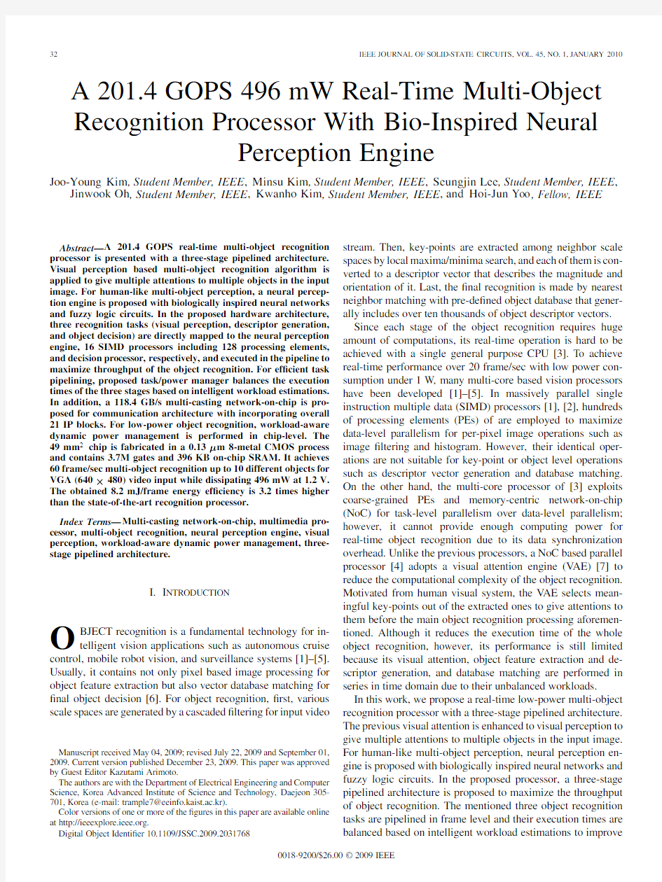
Fig.1.Visual perception based object recognition model.
pipelining ef?ciency.In addition,a multi-casting NoC is pro-posed for the integration of overall 21IP blocks of the processor.For low power consumption,workload-aware dynamic power management is performed in chip-level.As a result,the pro-posed processor achieves 60frame/sec 496mW multi-object
recognition up to 10different objects for VGA
(640
480)sized video input.
The rest of this paper is organized as follows.Section II de-scribes a visual perception based multi-object recognition algo-rithm in detail.Then,Section III explains system architecture of the proposed processor.Detailed designs of each building block are explained in Section IV.Section V describes the proposed NoC communication architecture.The chip implementation and evaluation results follow in Section VI.Finally,Section VII summarizes the paper.
II.V ISUAL P ERCEPTION B ASED M ULTI -O BJECT R ECOGNITION A.Visual Perception Based Object Recognition Model
Fig.1shows the concept diagram of the proposed visual per-ception based multi-object recognition model.The visual per-ception is an extended mechanism of the previous visual atten-tion [4]to multi-object cases.Based on visual attention,it ad-ditionally selects the seed points of the objects and performs seeded region growing to detect the regions-of-interest (ROIs)for https://www.360docs.net/doc/0f386638.html,pared with the previous attention,the visual perception gives multiple attentions to multiple objects of the input image by highlighting ROI of each object.After the visual perception,the next object recognition tasks such as key-point extraction and database matching are performed with focusing only on the selected ROIs.By processing only critical regions out of the whole image,computational cost of the object recog-nition is also reduced in proportional to the area of selected ROIs.
B.Overall Algorithm
Fig.2shows the overall algorithm of the proposed multi-object recognition processor.It is divided into three stages by
the role of each stage:visual perception,descriptor generation,and object decision.This algorithm is devised to recognize around 50of?ce stuffs in real-time,which is applicable for autonomous mobile robot’s vision system.
The visual perception stage is proposed to estimate the ROIs of objects,a global feature of the image,in advance to main object recognition processing.Based on Itti’s visual attention model [8],it extracts not only static features such as intensity,color,and orientation,but also a dynamic feature such as motion vector from the down-scaled input image to generate saliency map.Based on this saliency map,the visual perception selects the seed points of objects and performs seeded region growing to detect ROI of each object [9].Finally,it determines the ROIs for multiple objects in a unit of
4040pixel sized tile,called a grid-tile.For the implementation of visual perception stage,a special hardware block with bio-inspired neural networks and fuzzy logic circuits is proposed to mimic operations of human visual system.
The descriptor generation stage extracts key-points of objects out of the selected ROI grid-tiles from the visual perception stage,and generates descriptor vectors for them.To this end,various algorithmic methods such as KLT,Harris-corner detector,af?ne transformations,and scale invariant feature transform (SIFT)exist [6].In our algorithm,the SIFT is se-lected because it is robust to noise injection as well as scale and rotation variances.For the implementation of descriptor generation stage,a parallel processor consisting of many pro-cessing units is adopted to tackle parallel and complex image processing tasks.To be applicable for various algorithms,each processing unit is designed as a programmable device.
The object decision stage determines the ?nal recognition re-sults by performing database matching for selected regions.It matches the descriptor vectors out of the descriptor generation stage with the object database including thousands of object vectors.A vector matching is to search the minimum distance vector out of the vectors in the database with an input inquiry vector.To accelerate these repeated vector matching operations,
Fig.2.Three-stage multi-object recognition algorithm.
dedicated vector distance calculation units are employed in the object decision stage.
Overall,the proposed algorithm employs grid-based ROI pro-cessing that divides the input image into a number of two-di-mensional(2-D)grid-tiles and performs the processing based on them.It enables?ne-grained ROI extraction of multiple ob-jects and reduces the effective processing area of input images. To evaluate the proposed algorithm,we perform experiments with50of?ce objects out of Columbia object image library (Coil-100)[10].It is applied to2400sample images that include random objects in natural background scenes,with a16384-entry database made by the SIFT.As a result,overall recog-nition rate by the proposed algorithm is measured as92%.For evaluations of the ROI detection by visual perception,true pos-itive rate that represents the ratio of correctly detected region out of ground truth ROI and false positive rate that represents the ratio of incorrectly detected region out of not interested re-gion[11]are measured as70%and5%,respectively.The visual perception barely affects the overall recognition rate while re-ducing the processing area of the images to32.8%on average.
III.S YSTEM A RCHITECTURE
Fig.3shows the overall block diagram of the proposed pro-cessor.It consists of21IP blocks:a neural perception engine (NPE),a SPU task/power manager(STM),16SIMD processor units(SPUs),a decision processor(DP),and two external memory interfaces.The NPE is responsible for the?rst visual perception stage.It extracts the ROI grid-tiles for each object and sends them to16SPUs for detailed image processing. The16SPUs,whose power domain is separated into four,are responsible for the second descriptor generation stage.They extract object features out of the selected ROIs and convert them to descriptor vectors.The descriptor vectors out of the 16SPUs are gathered at the DP.The DP accelerates the vector matching process of descriptor vectors for the third object decision stage.The STM is specially devised to distribute the tasks of the ROI grid-tiles from the NPE to the16SPUs and to manage them.It also controls the pipeline stages of the overall processor and manages four power domains of16SPUs.The overall21IP blocks are interconnected through the proposed multi-casting NoC.
To increase parallelism and hardware utilization of the pro-posed processor,the proposed three stages are executed in the pipeline in frame level as shown in Fig.4.The pipelined data are ROI grid-tiles and descriptor vectors between the?rst–second stage and second–third stage,respectively.Unlike the execu-tion time of the?rst visual perception stage is constant due to its ?xed computation amount,the execution time of the second de-scriptor generation and third object decision are varying with the number of ROI grid-tiles and descriptor vectors.In order to bal-ance the execution times of three stages,the STM estimates the workload of the following descriptor vector and object decision stage based on the number of extracted ROI grid-tiles and de-scriptor vectors,respectively,and controls their execution times using two pipeline time balancing schemes.
To control the execution time of the descriptor generation stage,the STM performs workload-aware task scheduling (W ATS)that differs the number of scheduling SPUs according to the stage’s input workload.Fig.5(a)shows the?ow chart of the W ATS.First,the STM measures the number of ROI grid-tiles from the NPE and classi?es it to one of N work-load levels divided by N-1threshold values.And then,the STM determines the number of operating SPUs according to the classi?ed workload level.Since it allocates the SPUs in
Fig.3.Overall block diagram of proposed
processor.
Fig.4.Three-stage pipelined architecture.
proportional to the amount of workload,the execution time of the overall descriptor generation stage is kept in constant.The overall execution time is adjusted by modifying threshold values of classi?cation process.By lowering threshold values,the execution time is decreased because more SPUs are as-signed for the same amount of workload.On the other hand,the execution time increases when threshold values become high,while the number of operating SPUs is reduced.
To control the execution time of object decision stage,the STM performs applied database size control (ADSC),shown in Fig.5(b).Based on the vector matching algorithm of the DP [12],the overall execution time of the object decision stage is
Fig.5.(a)Workload-aware task scheduling.(b)Applied database size
control.
Fig.6.Block diagram of neural perception engine and SPU task/power manager.
proportional to the number of input descriptor vectors and the size of applied database.Based on these,the execution time of the object decision stage can be controlled by con?guring coverage rate of database.First,the STM measures the number of descriptor vectors from the SPUs and calculates the expected execution time of the vector matching.Then,it compares the expected execution time with the target pipeline time and con?gures the database coverage rate of the DP to meet the pipeline time.However,reducing coverage rate should be care-fully performed because it can degrade the overall recognition rate.With a 16384-entry database for 50objects recognition,correctly matched rate degrades 0.6%and 1.3%,when the coverage rate is 0.95and 0.90,respectively.With the help of the WATS and ADSC,the execution times of the three stages can be balanced to the target pipeline time,16ms,even under
the workload variations.As a result,the proposed processor achieves 60frame/sec frame-rate for VGA
(640480)sized video input.
IV .B UILDING B LOCK D ESIGN
A.Neural Perception Engine
Fig.6shows the block diagram of the NPE.For ef?cient ROI detection,the NPE employs a 32-bit RISC controller and three hardware engines;motion estimator (ME),visual attention en-gine (V AE),and object detection engine (ODE).The ME is em-ployed to extract dynamic motion vectors between two sequen-tial frames and implemented by array PEs with a full search block matching method [13].The V AE is employed to extract
Fig.7.Detailed visual perception algorithm.
static features such as intensity,color,and orientation and gen-erate the saliency map that combines the extracted feature maps through repeated normalizations.The ODE is proposed to per-form the ?nal ROI classi?cation for each object using the gener-ated saliency map.The RISC controller takes a role in control-ling the three dedicated engines and performing software ori-ented operations between the dedicated operations of the en-gines.A 24KB memory is used for storing original images and data communication among the three engines by sharing inter-mediate processing data.After the ?nal ROI classi?cation,the NPE transfers information of the obtained ROI grid-tiles to the STM through a FIFO queue.
Fig.7shows the detailed visual perception algorithm oper-ated by the NPE,which broadly consist of saliency map gen-eration and ROI classi?cation.The saliency map generation is mainly based on Itti’s saliency based visual attention [8]and ac-celerated by the V AE.First,the RGB channels of VGA sized
input image are down-sized to
80
60pixels and an inten-sity feature map and two color feature maps are generated by per-pixel ?ltering operations.Four orientation feature maps,for the direction of 0,45,90,and 135,are generated from the in-tensity feature map with the Gabor ?ltering.After generating multi-scale Gaussian pyramid images for each of 7maps,each image is transformed by a center-surround mechanism to en-hance the parts of the image that differ from their surround-ings.Finally,the saliency map is generated by repeated com-bination of normalized feature maps.The motion vector map,generated by the ME,is also combined in this step.Among these processes,computationally intensive image ?ltering op-erations such as Gabor,Gaussian,and center-surround ?ltering are accelerated by the hardware accelerator V AE.The normal-ization processes,which include irregular operations and can be performed in different ways,are performed by software by the RISC controller.After saliency map generation,ROI classi?ca-tion is performed by the ODE.First,the 10most salient points are selected as the seed points out of the saliency map.Then,from the most salient seed point,the ROI of an object grows from neighbor pixels of the seed through repeated homogeneity classi?cations.For the classi?cation of each pixel,an intensity,saliency,and location are used for homogeneity evaluation.The similarities between the seed and target pixel are measured for above three metrics,and based on the summated result,the ?nal classi?cation that the target pixel is determined to be joined to the ROI or not is determined.In case that the other seed points are included by the grown region,they are inhibited from the seed points in the next ROI classi?cation.After repeating clas-si?cation processes for 10seed points,the ROI of each object in pixel unit is quantized to the small sized grid-tile unit.
In the design of the V AE and ODE,biologically inspired cel-lular neural networks and neuro-fuzzy classi?er are employed for fast feature extraction and robust classi?cation,respectively.In the V AE,2-D cellular neural networks are used to rapidly ex-tract various features from the input image using its regional and collective processing [7].Fig.8shows overall block di-agram,circuits,and measured waveforms of the ODE.It em-ploys Gaussian fuzzy membership and single-layer neural net-
Fig.8.Block diagram,circuits,and measured waveforms of object detection engine.
work for similarity measure and decision making,respectively.In circuit design,the ODE exploits analog-based mixed-mode circuits to reduce area and power overhead of Gaussian func-tion circuits and neural synaptic multipliers.Except the digitally implemented learning part,data processing parts of the ODE are implemented by analog circuits.To exploit the analog data processing,8-bit intensity,saliency,and location values of the target and seed pixel are converted to analog signals by DACs.After that,three Gaussian function circuits measure the simi-larities between the two pixels for three metrics.A Gaussian function circuit is realized by the combination of MOS differ-ential pair and minimum follower circuit in current mode con-?guration.The differential pair circuit outputs the symmetric differential signals,each of which has exponential non-linearity characteristics.And the minimum follower circuit generates the Gaussian-like output by following the minimum between the symmetric differential signals.A 2-D Gaussian function circuit can be implemented by two consecutive Gaussian function cir-cuits by connecting the output of a Gaussian function circuit to the bias current input tail of the next Gaussian function circuit.Finally,current-mode neural synaptic circuits merge the three measured similarities with multiplying their weight values,and comparator circuit make the ?nal decision through thresholding.With a Hebbian learning [14],the weight values of the neural synaptic circuits,which play a role in classi?cation criteria,are updated every cycle.As a result,the ODE completes the ROI detection for 1object within
7s at 200MHz operating frequency.And its analog-based mixed-mode implementation reduces the area and power consumption by 59%and 44%,respectively,compared with those of digital implementation.
Fig.8also shows the measurement waveforms of mixed-mode ODE.They include DAC output signal,Gaussian function cir-cuit output signal,and ?nal classi?cation signal.As shown in the enlarged waveforms,the Gaussian output signal varies with the similarity of two analog input signals,and the ?nal classi?-cation signal is made based on it.B.SIMD Processor Unit
The SPU is designed to accelerate parallel image processing tasks of the descriptor generation stage.As shown in Fig.9,the SPU consist of a SPU controller,eight SIMD controlled dual-issued very long instruction word (VLIW)PEs,128-bit-wide data memory,and 2-D DMA.The eight PEs perform pixel parallel image processing operation such as Gaussian ?ltering,local maximum search,and histogram operation.The SPU con-troller controls the overall program ?ow of the SPU,decodes the instruction for the eight PEs,and performs data transfer between the eight PEs and data memory.For the data memory of the eight PEs,a 128-bit uni?ed memory is used rather than eight 16-bit memories to reduce the area and power consumption by 30.4%and 36.4%,respectively.The two data aligners between the data memory and eight PEs facilitate the data movement by rotating the uni?ed 128-bit data in 16-bit unit.The 2-D DMA performs the data transfer between the external memory and internal data memory in parallel with the PE operation.It automatically gen-erates the addresses for 2-D data access for the data transactions of vision applications.
The detailed block diagram of each dual-issued VLIW PE is also shown in Fig.9.It consists of two independent data
Fig.9.SIMD processor unit and its dual-issued VLIW PE.
paths for data processing operations such as ALU,shift,mul-tiply,and multiply-and-accumulation(MAC),and data transfer operations such as load and store.A51-bit dual-issued VLIW instruction enables parallel execution of the data processing and data transfer operation for every cycle.Utilizing its own reg-ister?le with?ve-read and three-write ports,the PE can exe-cute complex instructions for image processing such as two-way multiply/MAC,three-operanded min/max compare,and32-bit accumulation in a single cycle.The register?les of the other PEs can be directly accessed for window based image processing.In addition,each PE can be conditionally executed for the same in-struction using its independently managed status register.
C.Decision Processor
The object decision stage is composed of repeated vector matching processes that search the nearest vector of each input descriptor among object database.These repeated vector matching can be a performance bottleneck because distance calculations between the input vector and each of thousands of vectors in database require a lot of processing time.In the proposed processor,the DP accelerates the vector matching to make the object decision stage to be operated over60frame/sec frame rate for the database including more than15,000vectors. To reduce the search region of database without accuracy loss, the DP exploits the H-VQ algorithm presented in the previous vector matching processor[12].However,as shown in Fig.10, the hardware is redesigned to increase the throughput of vector matching with two modi?cations.First,the H-VQ algorithm is performed with dedicated three-stage pipelined datapath for vector distance calculation and comparison.Second,the bandwidth of database vector memory is increased twice,from 256-bit to512-bit.For the vector matching operations of the DP,descriptor vectors are gathered in feature vector memory from the SPUs as the?rst step.Then,the H-VQ algorithm is performed by a controller with the dedicated datapath.Once an input inquiry vector is set,the DP can obtain the index of the minimum distance vector by reading vectors from the database memory because the distance calculations and minimum vector updates are automatically performed in pipelined datapath stages.Since the DP can read two256-bit vectors from the database memory in a single cycle,the throughput of the DP is two vector distance calculations per cycle at200MHz. In overall,the DP matches256descriptor vectors with a 16384-entry database within3M cycles.
Fig.10.Block diagram of decision processor.
V .M ULTI -C ASTING N ETWORK -ON -C HIP
As the number of IP blocks increases to address computing requirements of recent multimedia processing,conventional shared medium based communication reveals its limitations to handle simultaneous data transactions among multiple IP blocks.As an alternative,a network-on-chip (NoC)is high-lighted as suitable communication architecture in multi-core era in spite of its high implementation costs compared with conventional bus,because it provides suf?cient bandwidth to multiple IP blocks and has good scalability with distributed router switches [15]–[17].In this processor,a multi-casting network-on-chip (MC-NoC)is proposed to integrate all of 21IP blocks.To cope with the processor’s application-driven data transactions such as 1-to-N broad/multi-casting and inter-pro-cessor data communications,the MC-NoC has a new combined architecture and supports a multi-casting capability.
Fig.11shows the proposed MC-NoC architecture that con-sists of a
910system network and four
77SPU cluster (SPC)networks.The 16SPUs are connected to the system network through the four SPC networks while the NPE,STM,DP,and two external interfaces are directly connected to the system network.It adopts a hierarchical star topology [15]as a basic topology for low latency data communications,and then,supplements a ring topology to the SPC networks for high-speed inter-SPU data transactions.The additional network links for the combined topology provides 25.6GB/s aggregated bandwidth between the SPC networks and allows each SPU to access the other SPUs in neighbor clusters in two switch hops.In overall,topology-combined MC-NoC provides a 118.4GB/s total bandwidth with the switch hop latency of less than 3.The proposed MC-NoC adopts a wormhole routing protocol whose packet is composed of header,address,and data ?ow control units (FLITs).Each FLIT consists of 2-bit control signals and 34-bit data signals including 2-bit FLIT type indicator.The header FLIT contains all information for the entire packet transmission such as 4-bit burst length for burst data
transaction
Fig.11.Proposed multi-casting NoC architecture.
up to eight FLITs and 2-bit priority level for quality-of-service.The 16-bit source de?ned routing information (RI)allows four switch traversals for normal packets and multi-casting to arbi-trary SPUs for multi-casting packets.In case of multi-casting packets,each bit of 16-bit RI indicates each destination SPU.In the MC-NoC,multi-casting from the NPE/STM to the 16SPUs is supported to accelerate 1-to-N data transactions such as program kernel distribution and image data download.To this end,each network switch is designed to have multi-casting ability.Fig.12shows a four-stage pipelined multi-casting crossbar switch and its multi-casting port.It consists of input ports,arbiters,mux based crossbar fabric,and output ports.At ?rst,the incoming FLITs are buffered at the 8-depth FIFO queue that contains the synchronization interface [18]for heterogeneous clock domain conversion.Then,each active input port sends a request signal to its destination arbiter to get a grant signal to traverse the crossbar fabric.For scheduling of grant signals,the arbiters perform a simple round-robin sched-uling according to the priority levels.In case of multi-casting
Fig.12.Four-stage pipelined multi-casting switch and its multi-casting port.
packet,a multi-casting input port sends multiple requests to all destination arbiters at the same time and waits until all grant signals are returned.To this end,in the multi-casting input port,a multi-port requester decodes the 16-bit RI and generates corresponding request signals and a grant checker holds the multi-casting packet until the registered request signals are equal to the received grant signals.After all grants are gathered,multi-casting is performed using the existing broad-casted wires of crossbar fabric without any additional wires.A vari-able strength driver is specially employed for the multi-casting port to provide suf?cient driving strength for multi-casting.As a result,the MC-NoC’s multi-casting capability accelerates the program kernel distribution and image data download task of the target object recognition by
6.56and
1.22,respectively.
VI.L OW -P OWER T ECHNIQUES
To reduce power consumption during the object recognition processing,chip-level power management is performed by the STM.Fig.13shows power management architecture of the proposed processor and its workload-aware dynamic power management.In the chip,power domain of the 16SPUs is divided into four domains and each of them is independently controlled by the STM.To control the power domains,off-chip power gating method [19]is employed for low cost implemen-tation.An external regulator with enable signal is employed for each of the power domains.The rest parts of the chip,the NPE,STM,DP and NoC,are placed in always-on domain.For ef?cient power gating of the chip,workload-aware power gating (W APG)is adopted with workload-aware task sched-uling (W ATS).When the STM measures the workload of the SPUs based on the number of ROI grid-tiles and determines the number of activating SPUs,it also determines the number of activated power domains in proportional to the workload amount,as shown in the ?ow chart of Fig.13.After that,the STM sends request signals to external regulators to gate unused power domains of SPUs before it assigns the ROI grid-tile tasks to the SPUs.Considering a few hundreds
of s settling time of external regulators,the requests for power gating occur only once per frame.By the WAPG,the number of activated power domains adaptively varies according to the workload of input frame as shown in Fig.13.
For further reduction of dynamic power in activated power domains,software controlled clock gating is applied to each op-erating SPU as shown in Fig.14.The clock of SPU can be gated by two software requests,end request and wait request .Each request is made by writing operation of the SPU to pre-de?ned address.The end request occurs when the SPU has ?nished its assigned task.On the other hand,the wait request is generated in situation that the SPU should stop its operation and wait for other module’s operation.To this end,the SPU writes the index value at the pre-de?ned wait address to notify the index of wait
Fig.13.Workload-aware dynamic power
management.
Fig.14.Software controlled clock gating.
conditions to be resolved.In this case,the clock is automati-cally restored when all the wait conditions are resolved.With the WAPG and software controlled clock gating,the power con-sumption of the 16SPUs is reduced by 38%,from 542mW to 336mW,while the power consumption of the overall processor amounts to 496mW at 60frame/sec frame-rate.
VII.C HIP I MPLEMENTATION AND E V ALUATION
The proposed recognition processor is fabricated in a
0.13m
1-poly 8-metal CMOS technology and
its
mm chip con-tains 36.4M transistors including 3.7M logic gates and 396KB on-chip SRAM.Fig.15shows the chip micrograph and Table I summarizes its features.The operating frequency is 200MHz for IP blocks and 400MHz for the NoC.Its peak performance amounts to 201.4giga operations per second (GOPS)when 695mW is dissipated.Speci?cally,128PEs of 16SPUs,each of which performs up to ?ve operations per cycle with a two-way MAC instruction,performs 128GOPS.The NPE performs
54
Fig.15.Chip micrograph.
GOPS;40linear PEs of the V AE perform 24GOPS,four parallel analog-digital mixed datapaths of the ODE perform 20GOPS,parallel SAD units of the ME perform 9.8GOPS,and a con-trol RISC performs 0.2GOPS.The DP performs 19.4GOPS using its 3216-bit SAD distance calculation and compare units.The average power consumption of the processor is 496mW at the supply voltage of 1.2V while the proposed multi-object recognition is running at 60frame/sec frame-rate.Table II shows power break-down of the proposed processor.The 16SPUs ac-count for about two thirds of overall power consumption.
Fig.16shows performance comparisons of the proposed pro-cessor with previous vision processors [2]–[4],[20].Fig.16(a)shows power ef?ciency comparison.The GOPS/W,which normalizes the GOPS performance with the power,is adopted as a performance index where the 1operation means 16-bit ?xed-point operation.The proposed processor achieves 290GOPS/W,which is 1.36times higher than the previous vision processors.Fig.16(b)shows energy ef?ciency comparison in object recognition,which is obtained by energy consumption per each frame.With 60frame/sec operation by the pipelined architecture and under 0.5W power consumption by the workload-aware dynamic power management,the proposed
Fig.16.(a)GOPS/W comparison.(b)Energy/frame
comparison.
Fig.17.Demonstration system.
TABLE I C HIP S
UMMARY
TABLE II
P OWER B REAK -D
OWN
processor achieves 8.2mJ energy dissipation per frame for VGA sized video input,which is 3.2times lower than the best of the previous object recognition processor.
For the validation of the fabricated chip,a demonstration system for real-time object recognition is developed as shown in Fig.17.It is composed of target objects,video camcorder,evaluation board,and LCD display.The evaluation board is composed of three ?oors,which are for host processor,video decoder and fabricated recognition chip,and peripheral interfaces such as LCD display,serial,USB,and Ethernet,respectively.In the demonstration system,the fabricated chip is used as a vision processing accelerator while the host processor controls the whole program sequences and accesses peripheral modules to display the results and to interface with the external devices.The overall object recognition is performed by three steps.First,the input image of the target objects is captured from the video camcorder and decoded to three-channel RGB pixel data by the video decoder.Then,the decoded image frame is processed by the proposed multi-object recognition https://www.360docs.net/doc/0f386638.html,st,the ?nal recognition results are displayed with the key-points at the LCD screen by the host processor.
VIII.C ONCLUSION
In this work,we have proposed a real-time multi-object recognition processor with a three-stage pipelined architec-ture.The visual perception based multi-object recognition algorithm has been developed to give multiple attentions to multiple objects in the input image.For human-like multi-ob-ject perception,a neural perception engine has been proposed with biologically inspired neural networks and fuzzy logic
circuits.In hardware architecture,a three-stage pipelined ar-chitecture has been proposed to maximize the throughput of recognition processing.The three object recognition tasks are executed in the pipeline and the execution times of the three tasks are balanced for ef?cient pipelining based on intelligent workload estimations.In addition,a 118.4GB/s multi-casting network-on-chip has been proposed for communication archi-tecture with incorporating overall 21IP blocks of the processor.Finally,workload-aware dynamic power management was performed for low-power object recognition.The 49mm chip contains 3.7M gates and 396KB on-chip SRAM in a
0.13m CMOS process.With a demonstration system,the fabricated chip achieves 60frame/sec multi-object recognition
up to 10different objects for VGA
(640
480)video input while dissipating 496mW at 1.2V.The obtained 8.2mJ/frame energy dissipation is 3.2times lower than the state-of-the-art recognition processor.
R EFERENCES
[1]S.Kyo et al.,“A 51.2GOPS scalable video recognition processor for
intelligent cruise control based on a linear array of 1284-way VLIW processing elements,”IEEE J.Solid-State Circuits ,vol.38,no.11,pp.1992–2000,Nov.2003.
[2]A.Abbo et al.,“XETAL-II:A 107GOPS,600mW massively-parallel
processor for video scene analysis,”IEEE J.Solid-State Circuits ,vol.43,no.1,pp.192–201,Jan.2008.
[3]D.Kim et al.,“An 81.6GOPS object recognition processor based on
NoC and visual image processing memory,”in Proc.IEEE Custom In-tegrated Circuits Conf.(CICC),Apr.2007,pp.443–446.
[4]K.Kim et al.,“A 125GOPS 583mW network-on-chip based parallel
processor with bio-inspired visual attention engine,”IEEE J.Solid-State Circuits ,vol.44,no.1,pp.136–147,Jan.2009.
[5]J.-Y.Kim et al.,“A 201.4GOPS 496mW real-time multi-object recog-nition processor with bio-inspired neural perception engine,”in IEEE ISSCC Dig.Tech.Papers ,Feb.2009,pp.150–151.
[6]D.G.Lowe,“Distinctive image features from scale-invariant key-points,”ACM https://www.360docs.net/doc/0f386638.html,puter Vision ,vol.60,no.2,pp.91–110,Jan.2004.
[7]S.Lee et al.,“The brain mimicking visual attention engine:An 802
60digital cellular neural network for rapid global feature extraction,”in IEEE Symp.VLSI Circuits Dig.,Jun.2008,pp.26–27.
[8]L.Itti et al.,“A model of saliency-based visual attention for rapid scene
analysis,”IEEE Trans.Pattern Anal.Machine Intell.,vol.20,no.11,pp.1254–1259,Nov.1998.
[9]M.Kim et al.,“A 22.8GOPS 2.83mW neuro-fuzzy object detection
engine for fast multi-object recognition,”in IEEE Symp.VLSI Circuits Dig.,Jun.2009,pp.260–261.
[10]S.A.Nene,S.K.Nayar,and H.Murase,Columbia Object Image Li-brary (Coil-100),Columbia University,New York,Technical Report CUCS-006-96,Feb.1996.
[11]S.Agarwal et al.,“Learning to detect objects in images via a sparse,
part-based representation,”IEEE Trans.Pattern Anal.Machine Intell.,vol.26,no.11,pp.1475–1490,Nov.2004.
[12]J.-Y.Kim et al.,“A 66frame/sec 38mW nearest neighbor matching
processor with hierarchical VQ algorithm for real-time object recogni-tion,”in Proc.IEEE A-SSCC ,Nov.2008,pp.177–180.
[13]P.Pirsch,N.Demassieux,and W.Gehrke,“VLSI architectures
for video compression—A survey,”Proc.IEEE ,vol.83,no.2,pp.220–246,Feb.1995.
[14]D.O.Hebb ,The Organization of Behavior .New York:Wiley,1949.[15]S.-J.Lee et al.,“An 800MHz star-connected on-chip network for ap-plication to systems on a chip,”in IEEE ISSCC Dig.Tech.Papers ,2003,pp.468–489.
[16]K.Lee et al.,“Low-power networks-on-chip for high-performance SoC
design,”IEEE Trans.VLSI Syst.,vol.14,no.2,pp.148–160,Feb.2006.[17]K.Kim et al.,“A 76.8GB/s 46mW low-latency network-on-chip for
real-time object recognition processor,”in Proc.IEEE A-SSCC ,Nov.2009,pp.177–180.
[18]J.N.Seizovic,“Pipeline synchronization,”in Proc.IEEE ASYNC ,Nov.
1994,pp.87–96.
[19]M.Keating et al.,Low Power Methodology Manual for System on Chip
Design .New York:Springer,2007.
[20]B.Khailany et al.,“A programmable 512GOPS stream processor for
signal,image,and video processing,”in IEEE ISSCC Dig.Tech.Pa-pers ,Feb.2007,pp.
272–273.
Joo-Young Kim (S’05)received the B.S.and M.S.degrees in electrical engineering and computer sci-ence from the Korea Advanced Institute of Science and Technology (KAIST),Daejeon,Korea,in 2005and 2007,respectively,and is currently working to-ward the Ph.D.degree in electrical engineering and computer science at KAIST.
Since 2006,he has been involved with the develop-ment of the parallel processors for computer vision.Currently,his research interests are parallel architec-ture,sub-systems,and VLSI implementation for bio-inspired vision
processor.
Minsu Kim (S’07)received the B.S.and M.S.de-grees in electrical engineering and computer science from the Korea Advanced Institute of Science and Technology (KAIST),Daejeon,Korea,in 2007and 2009,respectively.He is currently working toward the Ph.D.degree in electrical engineering and com-puter science at KAIST.
His research interests include network-on-chip based SoC design and bio-inspired VLSI architecture for intelligent vision
processing.
Seungjin Lee (S’06)received the B.S.and M.S.de-grees in electrical engineering and computer science from the Korea Advanced Institute of Science and Technology (KAIST),Daejeon,Korea,in 2006and 2008,respectively.He is currently working toward the Ph.D.degree in electrical engineering and com-puter science from KAIST.
His previous research interests include low-power digital signal processors for digital hearing aids and body area communication.Currently,he is investi-gating parallel architectures for computer vision pro-
cessing.
Jinwook Oh (S’08)received the B.S degree in elec-trical engineering and computer science from Seoul National University,Seoul,Korea,in 2008.He is cur-rently working toward the M.S.degree in electrical engineering and computer science at KAIST,Dae-jeon,Korea.
His research interests include low-power digital signal processors for computer vision.Recently,he is involved with the VLSI implementation of neural networks and fuzzy
logics.
Kwanho Kim (S’04)received the B.S.and M.S degrees in electrical engineering and computer science from the Korea Advanced Institute of Sci-ence and Technology (KAIST)in 2004and 2006,respectively.He is currently working toward the Ph.D.degree in electrical engineering and computer science at KAIST.
In 2004,he joined the Semiconductor System Laboratory (SSL)at KAIST as a Research Assistant.His research interests include VLSI design for object recognition,architecture and implementation of
NoC-based SoC.
Hoi-Jun Yoo(M’95–SM’04–F’08)graduated from
the Electronic Department of Seoul National Uni-
versity,Seoul,Korea,in1983and received the M.S.
and Ph.D degrees in electrical engineering from the
Korea Advanced Institute of Science and Technology
(KAIST),Daejeon,in1985and1988,respectively.
His Ph.D.work concerned the fabrication process
for GaAs vertical optoelectronic integrated circuits.
From1988to1990,he was with Bell Communi-
cations Research,Red Bank,NJ,where he invented
the two-dimensional phase-locked VCSEL array,the front-surface-emitting laser,and the high-speed lateral HBT.In1991,he be-came Manager of a DRAM design group at Hyundai Electronics and designed a family of from fast-1M DRAMs and256M synchronous DRAMs.In1998 he joined the faculty of the Department of Electrical Engineering at KAIST and now is a full Professor.From2001to2005,he was the Director of the System In-tegration and IP Authoring Research Center(SIPAC),funded by Korean govern-ment to promote worldwide IP authoring and its SOC application.From2003to 2005,he was the full time Advisor to Minister of Korea Ministry of Information and Communication and National Project Manager for SoC and Computer.In 2007,he founded SDIA(System Design Innovation and Application Research Center)at KAIST to research and develop SoCs for intelligent robots,wearable computers and bio systems.His current interests are high-speed and low-power network on chips,3-D graphics,body area networks,biomedical devices and circuits,and memory circuits and systems.He is the author of the books DRAM Design(Seoul,Korea:Hongleung,1996;in Korean),High Performance DRAM (Seoul,Korea:Sigma,1999;in Korean),and chapters of Networks on Chips (New York:Morgan Kaufmann,2006).
Dr.Yoo received the Electronic Industrial Association of Korea Award for his contribution to DRAM technology the1994,Hynix Development Award in 1995,the Korea Semiconductor Industry Association Award in2002,Best Re-search of KAIST Award in2007,Design Award of2001ASP-DAC,and Out-standing Design Awards2005,2006,2007A-SSCC.He is a member of the executive committees of ISSCC,Symposium on VLSI,and A-SSCC,and was the TPC chair of the A-SSCC2008.
变电所母线桥的动稳定校验
变电所母线桥的动稳定校验 随着用电负荷的快速增长,许多变电所都对主变进行了增容,并对相关设备进行了调换和校验,但往往会忽视主变母线桥的动稳定校验,事实上此项工作非常重要。当主变增容后,由于阻抗发生了变化,短路电流将会增大许多,一旦发生短路,产生的电动力有可能会对母线桥产生破坏。特别是户内母线桥由于安装时受地理位置的限制,绝缘子间的跨距较长,受到破坏的可能性更大,所以应加强此项工作。 下面以我局35kV/10kv胡店变电所#2主变增容为例来谈谈如何进行主变母线桥的动稳定校验和校验中应注意的问题。 1短路电流计算 图1为胡店变电所的系统主接线图。(略) 已知#1主变容量为10000kVA,短路电压为7.42%,#2主变容量为12500kVA,短路电压为7.48%(增容前短路电压为7.73%)。 取系统基准容量为100MVA,则#1主变短路电压标么值 X1=7.42/100×100×1000/10000=0.742, #2主变短路电压标么值 X2=7.48/100×100×1000/12500=0.5984 胡店变电所最大运行方式系统到35kV母线上的电抗标么值为0.2778。 ∴#1主变与#2主变的并联电抗为: X12=X1×X2/(X1+X2)=0.33125; 最大运行方式下系统到10kV母线上的组合电抗为: X=0.2778+0.33125=0.60875
∴10kV母线上的三相短路电流为:Id=100000/0.60875*√3*10.5,冲击电流:I sh=2.55I =23032.875A。 d 2动稳定校验 (1)10kV母线桥的动稳定校验: 进行母线桥动稳定校验应注意以下两点: ①电动力的计算,经过对外边相所受的力,中间相所受的力以及三相和二相电动力进行比较,三相短路时中间相所受的力最大,所以计算时必须以此为依据。 ②母线及其支架都具有弹性和质量,组成一弹性系统,所以应计算应力系数,计及共振的影响。根据以上两点,校验过程如下: 已知母线桥为8×80mm2的铝排,相间中心线间距离为210mm,先计算应力系数: ∵频率系数N f=3.56,弹性模量E=7×10.7 Pa,单位长度铝排质量M=1.568kg/m,绝缘子间跨距2m,则一阶固有频率: f’=(N f/L2)*√(EI/M)=110Hz 查表可得动态应力系数β=1.3。 ∴单位长度铝排所受的电动力为: f ph=1.73×10⁻⁷I sh2/a×β=568.1N/m ∵三相铝排水平布置,∴截面系数W=bh2/6=85333mm3,根据铝排的最大应力可确定绝缘子间允许的最大跨距为: L MAX=√10*σal*W/ f ph=3.24m ∵胡店变主变母线桥绝缘子间最大跨距为2m,小于绝缘子间的最大允许跨距。
数据挖掘算法综述
数据挖掘方法综述 [摘要]数据挖掘(DM,DataMining)又被称为数据库知识发现(KDD,Knowledge Discovery in Databases),它的主要挖掘方法有分类、聚类、关联规则挖掘和序列模式挖掘等。 [关键词]数据挖掘分类聚类关联规则序列模式 1、数据挖掘的基本概念 数据挖掘从技术上说是从大量的、不完全的、有噪声的、模糊的、随机的数据中提取隐含在其中的、人们事先不知道的、但又是潜在的有用的信息和知识的过程。这个定义包括好几层含义: 数据源必须是真实的、大量的、含噪声的、发现的是用户感兴趣的知识, 发现的知识要可接受、可理解、可运用, 并不要求发现放之四海皆准的知识, 仅支持特定的发现问题, 数据挖掘技术能从中自动分析数据进行归纳性推理从中发掘出潜在的数据模式或进行预测, 建立新的业务模型帮助决策者调整策略做出正确的决策。数据挖掘是是运用统计学、人工智能、机器学习、数据库技术等方法发现数据的模型和结构、发现有价值的关系或知识的一门交叉学科。数据挖掘的主要方法有分类、聚类和关联规则挖掘等 2、分类 分类(Classification)又称监督学习(Supervised Learning)。监
督学习的定义是:给出一个数据集D,监督学习的目标是产生一个联系属性值集合A和类标(一个类属性值称为一个类标)集合C的分类/预测函数,这个函数可以用于预测新的属性集合(数据实例)的类标。这个函数就被称为分类模型(Classification Model),或者是分类器(Classifier)。分类的主要算法有:决策树算法、规则推理、朴素贝叶斯分类、支持向量机等算法。 决策树算法的核心是Divide-and-Conquer的策略,即采用自顶向下的递归方式构造决策树。在每一步中,决策树评估所有的属性然后选择一个属性把数据分为m个不相交的子集,其中m是被选中的属性的不同值的数目。一棵决策树可以被转化成一个规则集,规则集用来分类。 规则推理算法则直接产生规则集合,规则推理算法的核心是Separate-and-Conquer的策略,它评估所有的属性-值对(条件),然后选择一个。因此,在一步中,Divide-and-Conquer策略产生m条规则,而Separate-and-Conquer策略只产生1条规则,效率比决策树要高得多,但就基本的思想而言,两者是相同的。 朴素贝叶斯分类的基本思想是:分类的任务可以被看作是给定一个测试样例d后估计它的后验概率,即Pr(C=c j︱d),然后我们考察哪个类c j对应概率最大,便将那个类别赋予样例d。构造朴素贝叶斯分类器所需要的概率值可以经过一次扫描数据得到,所以算法相对训练样本的数量是线性的,效率很高,就分类的准确性而言,尽管算法做出了很强的条件独立假设,但经过实际检验证明,分类的效果还是
数据挖掘概述
数据挖掘概述 阅读目录 ?何为数据挖掘? ?数据挖掘背后的哲学思想 ?数据挖掘的起源 ?数据挖掘的基本任务 ?数据挖掘的基本流程 ?数据挖掘的工程架构 ?小结 回到顶部何为数据挖掘? 数据挖掘就是指从数据中获取知识。 好吧,这样的定义方式比较抽象,但这也是业界认可度最高的一种解释了。对于如何开发一个大数据环境下完整的数据挖掘项目,业界至今仍没有统一的规范。说白了,大家都听说过大数据、数据挖掘等概念,然而真正能做而且做好的公司并不是很多。
笔者本人曾任职于A公司云计算事业群的数据引擎团队,有幸参与过几个比较大型的数据挖掘项目,因此对于如何实施大数据场景下的数据挖掘工程有一些小小的心得。但由于本系列博文主要是结合传统数据挖掘理论和笔者自身在A云的一些实践经历,因此部分观点会有较强主观性,也欢迎大家来跟我探讨。 回到顶部数据挖掘背后的哲学思想 在过去很多年,首要原则模型(first-principle models)是科学工程领域最为经典的模型。 比如你要想知道某辆车从启动到速度稳定行驶的距离,那么你会先统计从启动到稳定耗费的时间、稳定后的速度、加速度等参数;然后运用牛顿第二定律(或者其他物理学公式)建立模型;最后根据该车多次实验的结果列出方程组从而计算出模型的各个参数。通过该过程,你就相当于学习到了一个知识--- 某辆车从启动到速度稳定行驶的具体模型。此后往该模型输入车的启动参数便可自动计算出该车达到稳定速度前行驶的距离。 然而,在数据挖掘的思想中,知识的学习是不需要通过具体问题的专业知识建模。如果之前已经记录下了100辆型号性能相似的车从启动到速度稳定行驶的距离,那么我就能够对这100个数据求均值,从而得到结果。显然,这一过程是是直接面向数据的,或者说我们是直接从数据开发模型的。 这其实是模拟了人的原始学习过程 --- 比如你要预测一个人跑100米要多久时间,你肯定是根据之前了解的他(研究对象)这样体型的人跑100米用的多少时间做一个估计,而不会使用牛顿定律来算。 回到顶部数据挖掘的起源 由于数据挖掘理论涉及到的面很广,它实际上起源于多个学科。如建模部分主要起源于统计学和机器学习。统计学方法以模型为驱动,常常建立一个能够产生数据的模型;而机器学习则以算法为驱动,让计算机通过执行算法来发现知识。仔细想想,"学习"本身就有算法的意思在里面嘛。
母线电动力及动热稳定性计算
母线电动力及动热稳定性计算 1 目的和范围 本文档为电气产品的母线电动力、动稳定、热稳定计算指导文件,作为产品结构设计安全指导文件的方案设计阶段指导文件,用于母线电动力、动稳定性、热稳定性计算的选型指导。 2 参加文件 表1 3 术语和缩略语 表2 4 母线电动力、动稳定、热稳定计算 4.1 载流导体的电动力计算 4.1.1 同一平面内圆细导体上的电动力计算
? 当同一平面内导体1l 和2l 分别流过1I 和2I 电流时(见图1),导体1l 上的电动力计 算 h F K I I 4210 π μ= 式中 F ——导体1l 上的电动力(N ) 0μ——真空磁导率,m H 60104.0-?=πμ; 1I 、2I ——流过导体1l 和2l 的电流(A ); h K ——回路系数,见表1。 图1 圆细导体上的电动力 表1 回路系数h K 表 两导体相互位置及示意图 h K 平 行 21l l = ∞=1l 时,a l K h 2= ∞≠1l 时,?? ? ???-+=l a l a a l K h 2)(12 21l l ≠ 22 2) ()(1l a m l a l a K h ++-+= 22)()1(l a m +-- l a m =
? 当导体1l 和2l 分别流过1I 和2I 电流时,沿1l 导体任意单位长度上各点的电动力计 算 f 124K f I I d μ= π 式中 f ——1l 导体任意单位长度上的电动力(m N ); f K ——与同一平面内两导体的长度和相互位置有关的系数,见表2。 表2 f K 系数表
4.1.2 两平行矩形截面导体上的电动力计算 两矩形导体(母线)在b <<a ,且b >>h 的情况下,其单位长度上的电动力F 的 计算见表3。 当矩形导体的b 与a 和h 的尺寸相比不可忽略时,可按下式计算 712 210x L F I I K a -=? 式中 F -两导体相互作用的电动力,N ; L -母线支承点间的距离,m ; a -导体间距,m ; 1I 、2I -流过两个矩形母线的电流,A ; x K -导体截面形状系数; 表3 两矩形导体单位长度上的电动力 4.1.3 三相母线短路时的电动力计算
高压电缆热稳定校验计算书
筠连县分水岭煤业有限责任公司 井 下 高 压 电 缆 热 稳 定 性 校 验 计 算 书 巡司二煤矿 编制:机电科 筠连县分水岭煤业有限责任公司
井下高压电缆热稳定校验计算书 一、概述: 根据《煤矿安全规程》第453条及456条之规定,对我矿入井高压电缆进行热稳定校验。 二、确定供电方式 我矿高压供电采用分列运行供电方式,地面变电所、井下变电所均采用单母线分段分列供电方式运行,各种主要负荷分接于不同母线段。 三、井下高压电缆明细: 矿上有两趟主进线,引至巡司变电站不同母线段,一趟931线,另一趟925线。井下中央变电所由地面配电房10KV输入。 入井一回路:MYJV22-8.7/10KV 3*50mm2--800m(10KV) 入井二回路:MYJV22-8.7/10KV 3*50mm2--800m(10KV) 四、校验计算 1、井下入井回路高压电缆热稳定性校验 已知条件:该条高压电缆型号为,MYJV22-8.7/10KV 3*50mm2 ,800m,电缆长度为800m=0.8km。 (1)计算电网阻抗 查附表一,短路电流的周期分量稳定性为 电抗:X=0.072*0.8=0.0576Ω; 电阻:R=0.407*0.8=0.3256 Ω; (2)三相短路电流的计算
A Z I 5.174693305 .0310000 3v 3=?== ∞ (3)电缆热稳定校验 由于断路器的燃弧时间及固有动作时间之和约为t=0.05S; 查附表二得热稳定计算系数取K=142; 故电缆最小热值稳定截面为 23mm 51.2705.0142/5.17469t )/(min ===∞)(K I S Smin<50mm 2 故选用 MYJV 22 -8.7/10KV 3*50 电缆热稳定校验合格,符合要求。 附表一:三相电缆在工作温度时的阻抗值(Ω/Km ) 电缆截面S (mm 2 ) 4 6 10 16 2 5 35 50 70 95 120 150 185 240 交联聚乙烯 R 4.988 3.325 2.035 1.272 0.814 0.581 0.407 0.291 0.214 0.169 0.136 0.11 0.085 X 0.093 0.093 0.087 0.082 0.075 0.072 0.072 0.069 0.069 0.069 0.07 0.07 0.07 附表二 不同绝缘导体的热稳定计算系数 绝缘材料 芯线起始温度(° C ) 芯线最高允许温度(°C ) 系数K 聚氯乙烯 70 160 115(114) 普通橡胶 75 200 131 乙丙橡胶 90 250 143(142) 油浸纸绝缘 80 160 107 交联聚乙烯 90 250 142
数据挖掘分类算法介绍
数据挖掘分类算法介绍 ----------------------------------------------------------------------------------------------------------------------------- 分类是用于识别什么样的事务属于哪一类的方法,可用于分类的算法有决策树、bayes分类、神经网络、支持向量机等等。 决策树 例1 一个自行车厂商想要通过广告宣传来吸引顾客。他们从各地的超市获得超市会员的信息,计划将广告册和礼品投递给这些会员。 但是投递广告册是需要成本的,不可能投递给所有的超市会员。而这些会员中有的人会响应广告宣传,有的人就算得到广告册不会购买。 所以最好是将广告投递给那些对广告册感兴趣从而购买自行车的会员。分类模型的作用就是识别出什么样的会员可能购买自行车。 自行车厂商首先从所有会员中抽取了1000个会员,向这些会员投递广告册,然后记录这些收到广告册的会员是否购买了自行车。 数据如下:
在分类模型中,每个会员作为一个事例,居民的婚姻状况、性别、年龄等特征作为输入列,所需预测的分类是客户是否购买了自行车。 使用1000个会员事例训练模型后得到的决策树分类如下:
※图中矩形表示一个拆分节点,矩形中文字是拆分条件。 ※矩形颜色深浅代表此节点包含事例的数量,颜色越深包含的事例越多,如全部节点包含所有的1000个事例,颜色最深。经过第一次基于年龄的拆分后,年龄大于67岁的包含36个事例,年龄小于32岁的133个事例,年龄在39和67岁之间的602个事例,年龄32和39岁之间的229个事例。所以第一次拆分后,年龄在39和67岁的节点颜色最深,年龄大于67岁的节点颜色最浅。 ※节点中的条包含两种颜色,红色和蓝色,分别表示此节点中的事例购买和不购买自行车的比例。如节点“年龄>=67”节点中,包含36个事例,其中28个没有购买自行车,8个购买了自行车,所以蓝色的条比红色的要长。表示年龄大于67的会员有74.62%的概率不购买自行车,有23.01%的概率购买自行车。 在图中,可以找出几个有用的节点: 1. 年龄小于32岁,居住在太平洋地区的会员有7 2.75%的概率购买自行车; 2. 年龄在32和39岁之间的会员有68.42%的概率购买自行车; 3. 年龄在39和67岁之间,上班距离不大于10公里,只有1辆汽车的会员有66.08%的概率购买自行车;
热稳定性校验(主焦
井下高压开关、供电电缆动热稳定性校验 一、-350中央变电所开关断路器开断能力及电缆热稳定性校验 1 23 G 35kV 2 Uz%=7.5△P N.T =12kW △P N.T =3.11kW S N.T =8MVA 6kV S1点三相短路电流计算: 35kV 变压器阻抗: 2 22.1. u %7.5 6.30.37()1001008z N T N T U Z S ?===Ω? 35kV 变压器电阻:2 22.1.22. 6.30.0120.007()8 N T N T N T U R P S =?=?=Ω 35kV 变压器电抗:10.37()X = ==Ω 电缆电抗:02(x )0.415000.08780 0.66()1000 1000i L X ??+?== =Ω∑ 电缆电阻:02(x )0.11815000.118780 0.27()1000 1000 i L R ??+?== =Ω∑ 总阻抗: 21.370.66) 1.06( Z ==Ω S1点三相短路电流:(3)1 3.43()d I KA === S2点三相短路电流计算: S2点所用电缆为MY-3×70+1×25,长400米,变压器容量为500KV A ,查表的:(2)2d I =2.5KA
S2点三相短路电流:32 d d =2.88I I KA = 1、架空线路、入井电缆的热稳定性校验。已知供电负荷为3128.02KV A ,电压为6KV ,需用系数0.62,功率因数cos 0.78φ=,架空线路长度1.5km ,电缆长度780m (1)按经济电流密度选择电缆,计算容量为 3128.020.62 2486.37cos 0.78 kp S KVA φ?= ==。 电缆的长时工作电流Ig 为239.25 Ig === A 按长时允许电流校验电缆截面查煤矿供电表5-15得MYJV42-3×185-6/6截面长时允许电流为479A/6kV 、大于239.25A 符合要求。 (2)按电压损失校验,配电线路允许电压损失5%得 60000.1300Uy V ?=?=,线路的实际电压损失 109.1L U COS DS φφ?====,U ?小于300V 电压损失满足要求 (3)热稳定性条件校验,短路电流的周期分量稳定性为 电缆最小允许热稳定截面积: 3 2min d =S I mm 其中:i t ----断路器分断时间,一般取0.25s ; C----电缆热稳定系数,一般取100,环境温度35℃,电缆温升不超过120℃时,铜芯电缆聚乙烯电缆熔化温度为130℃,电
上海理工大学高等传热学试题及答案
1.试求出圆柱坐标系的尺度系数,并由此导出圆柱坐标系中的导热微分方程。 2 .一无限大平板,初始温度为T 0;τ>0时,在x = 0表面处绝热;在x = L 表面以对流方式向温度为t f 的流体换热。试用分离变量法求出τ>0时平板的温度分布(常物性)。(需求出特征函数、超越方程的具体形式,范数(模)可用积分形式表示)。(15分) , 3.简述近似解析解——积分法中热层厚度δ的概念。 答:近似解析解:既有分析解的特征:得到的结果具有解析函数形式,又有近似解的特征:结果只能近似满足导热解问题。在有限的时间内,边界温度 的变化对于区域温度场的影响只是在某一有限的范围内,把这个有限的范围定义为热层厚度δ。 4.与单相固体导热相比,相变导热有什么特点 答:相变导热包含了相变和导热两种物理过程。相变导热的特点是 1.固、液两相之间存在着 移动的交界面。 2.两相交界面有潜热的释放(或吸收) | 对流部分(所需量和符号自己设定) 1 推导极坐标系下二维稳态导热微分方程。 2 已知绕流平板流动附面层微分方程为 y u y u V x u u 22??=??+??ν 取相似变量为: x u y νη∞ = x u f νψ∞= 写出问题的数学模型并求问题的相似解。 3 已知绕流平板流动换热的附面层能量积分方程为: ?=∞?? =-δ00)(y y t a dy t t u dx d 当Pr<<1时,写出问题的数学模型并求问题的近似积分解及平均Nu (取三次多项式)。 4 ] O x
5写出常热流圆管内热充分发展流动和换热问题的数学模型并求出速度和温度分布及Nu x.辐射 1.请推导出具有n个表面的净热流法壁面间辐射换热求解公式,并简要说明应用任一种数值方法的求解过程。 2.试推导介质辐射传递方程的微分形式和积分形式,要求表述出各个步骤和结果中各个相关量的含义。 3.根据光谱辐射强度表示下面各量:1)光谱定向辐射力;2)定向辐射力;3)光谱辐射力;4)辐射力;5)辐射热流量。要求写清各量的符号、单位。 4.说明下列术语(可用数学表达式)(每题4分) a)光学厚度 b)漫有色表面 c)? d)兰贝特余弦定律 e)光谱散射相函数 f)定向“灰”入射辐射
高压电缆热稳定校验计算书
*作品编号:DG13485201600078972981* 创作者:玫霸* 筠连县分水岭煤业有限责任公司 井 下 高 压 电 缆 热 稳 定 性 校 验 计 算 书 巡司二煤矿
编制:机电科 筠连县分水岭煤业有限责任公司 井下高压电缆热稳定校验计算书 一、概述: 根据《煤矿安全规程》第453条及456条之规定,对我矿入井高压电缆进行热稳定校验。 二、确定供电方式 我矿高压供电采用分列运行供电方式,地面变电所、井下变电所均采用单母线分段分列供电方式运行,各种主要负荷分接于不同母线段。 三、井下高压电缆明细: 矿上有两趟主进线,引至巡司变电站不同母线段,一趟931线,另一趟925线。井下中央变电所由地面配电房10KV输入。 入井一回路:MYJV22-8.7/10KV 3*50mm2--800m(10KV) 入井二回路:MYJV22-8.7/10KV 3*50mm2--800m(10KV) 四、校验计算 1、井下入井回路高压电缆热稳定性校验 已知条件:该条高压电缆型号为,MYJV22-8.7/10KV 3*50mm2 ,800m,电缆长度为800m=0.8km。 (1)计算电网阻抗 查附表一,短路电流的周期分量稳定性为
电抗:X=0.072*0.8=0.0576Ω; 电阻:R=0.407*0.8=0.3256 Ω; (2)三相短路电流的计算 (3)电缆热稳定校验 由于断路器的燃弧时间及固有动作时间之和约为t=0.05S; 查附表二得热稳定计算系数取K=142; 故电缆最小热值稳定截面为 Smin<50mm2故选用 MYJV22 -8.7/10KV 3*50 电缆热稳定校验合格,符合要求。 附表一:三相电缆在工作温度时的阻抗值(Ω/Km)
大数据时代的数据挖掘技术
大数据时代的数据挖掘 技术 Document serial number【UU89WT-UU98YT-UU8CB-UUUT-UUT108】
大数据时代的数据挖掘技术 【摘要】随着大数据时代的到来,在大数据观念不断提出的今天,加强数据大数据挖掘及时的应用已成为大势所趋。那么在这一过程中,我们必须掌握大数据与数据挖掘的内涵,并对数据挖掘技术进行分析,从而明确大数据时代下数据挖掘技术的应用领域,促进各项数据的处理,提高大数据处理能力。 【关键词】大数据时代;数据挖掘技术;应用 大数据时代下的数据处理技术要求更高,所以要想确保数据处理成效得到提升,就必须切实加强数据挖掘技术的应用,才能更好地促进数据处理职能的转变,提高数据处理效率,以下就大数据时代下的数据挖掘技术做出如下分析。 1.大数据与数据挖掘的内涵分析 近年来,随着云计算和物联网概念的提出,信息技术得到了前所未有的发展,而大数据则是在此基础上对现代信息技术革命的又一次颠覆,所以大数据技术主要是从多种巨量的数据中快速的挖掘和获取有价值的信息技术,因而在云时代的今天,大数据技术已经被我们所关注,所以数据挖掘技术成为最为关键的技术。尤其是在当前在日常信息关联和处理中越来越离不开数据挖掘技术和信息技术的支持。大数据,而主要是对全球的数据量较大的一个概括,且每年的数据增长速度较快。而数据挖掘,主要是从多种模糊而又随机、大量而又复杂且不规则的数据中,获得有用的信息知识,从数据库中抽丝剥茧、转换分析,从而掌握其潜在价值与规律[1]。
2.大数据时代下数据挖掘技术的核心-分析方法 数据挖掘的过程实际就是对数据进行分析和处理,所以其核心就在于数据的分析方法。要想确保分析方法的科学性,就必须确保所采用算法的科学性和可靠性,获取数据潜在规律,并采取多元化的分析方法促进问题的解决和优化。以下就几种常见的数据分析方法做出简要的说明。 一是归类法,主要是将没有指向和不确定且抽象的数据信息予以集中,并对集中后的数据实施分类整理和编辑处理,从而确保所形成的数据源具有特征一致、表现相同的特点,从而为加强对其的研究提供便利。所以这一分析方法能有效的满足各种数据信息处理。 二是关联法,由于不同数据间存在的关联性较为隐蔽,采取人力往往难以找出其信息特征,所以需要预先结合信息关联的表现,对数据关联管理方案进行制定,从而完成基于某种目的的前提下对信息进行处理,所以其主要是在一些信息处理要求高和任务较为复杂的信息处理工作之中。 三是特征法,由于数据资源的应用范围较广,所以需要对其特征进行挖掘。也就是采用某一种技术,将具有相同特征的数据进行集中。例如采用人工神经网络技术时,主要是对大批量复杂的数据分析,对非常复杂的模式进行抽取或者对其趋势进行分析。而采取遗传算法,则主要是对其他评估算法的适合度进行评估,并结合生物进化的原理,对信息数据的成长过程进行虚拟和假设,从而组建出半虚拟、半真实的信息资源。再如可视化技术则是为数据挖掘提供辅助,采取多种方式对数据的
传热学上海理工大学硕士研究生入学考试试题
2004年上海理工大学硕士研究生入学考试试题考试科目:传热学准考证号:得分: 一、问答题(每题5分) 1. 一无内热源平板沿厚度x方向发生一维稳态导热,其一侧表面上的温度梯度 =30 ℃/m,导热系数λ1=40W/(m.℃),如果其另一侧表面上的导热系数λ2=50W/(m.℃),问这一侧表面上的温度梯度是多少? 2. 解释毕渥准则数Bi的物理含义,并说明为什么用Bi判别非稳态导热问题能否采用集总参数法求解。 3. 图1.1示出了常物性、有均匀内热源、二维稳态导热问题局部边界区域的网格配置,试用元体平衡法建立节点0关于温度t的有限差分方程式(设 ,所需参数的符号自己设定)。 4. 当条件相同时,物体在空气中冷却快还是在水中冷却快?这一现象说明对流换热与什么因素相关? 5. 试用简图表示流体沿平板流动时速度边界层的发展并说明速度边界层内分成哪些区域? 6. 试解释普朗特数Pr的物理意义,并示意性的画出Pr>1时的速度边界层和热边界层厚度沿板长的变化(速度边界层和热边界层要画在同一图上以便比较)。 7. 说明温度附面层的概念及附面层能量微分方程在物理上忽略了哪部分换热。 8. 在应用管内旺盛紊流实验关联式时,当流体与换热壁面温差较大时需要对计算结果修正,为什么? 9. 试说明为什么一个细长圆柱水平放置时自然对流换热一般大于竖直放置时的自然对流换热? 10.在稳定膜态沸腾过程中,为什么换热系数随 增加而迅速上升?
11.试说明大气中CO2含量增高为什么会出现大气温室效应? 二、计算题 1. (10分)一直径为5cm的钢球,其初始温度为500℃,突然被置于温度为 30℃的空气中。设钢球表面与周围环境的对流换热系数为10 W/m2℃,试计算钢球非稳态导热的时间常数及其被冷却到300℃所需的时间。已知钢球的比热为c=0.48kJ/kg℃, ρ=7753kg/m3, λ=33W/m℃。 2. (20分)长10m、外径133mm的水平管道通过一大房间,房间壁面及其内 的空气温度均为30℃。若管道表面温度为90℃、黑度为0.9,求管道的散 热量(自然对流换热的努塞尔特数用下式计算)。3. (22分)如图2所示为一半径R=1m的半球,球冠3绝热。底面1和2的 温度分别为500℃和100℃,黑度都为0.9,求底面1和2间的辐射散热量。 4. (23分)温度为95℃的热空气流经一内径100mm、厚度6mm的圆管,管 壁导热系数为22 W/m℃。管外环境温度为30℃,管外壁与环境的总换热系数为10 W/m2℃。若管内空气质量流量为407kg/h,求管出口空气温度降低到65℃时的管长(不需考虑修正)。 三、理论题 1.(8分)一厚度为2δ的无内热源薄平板,其导热系数和初始温度分别为 λ和t0,突然被插在温度为t f的流体中。平板表面与流体的换热系数为h,给出问题的完整数学描述。 2. (12分)绕流平板换热的附面层积分方程为: 平板温度为t W,来流速度和温度分别为u∞和t∞,若Pr<<1,可以忽略速
大数据技术概述
大数据技术 1.什么是数据挖掘,什么是机器学习: 什么是机器学习 关注的问题:计算机程序如何随着经验积存自动提高性能; 研究计算机如何样模拟或实现人类的学习行为,以猎取新的知识或技能,重新组织已有的知识结构使之不断改善自身的性能; 通过输入和输出,来训练一个模型。 2.大数据分析系统层次结构:应用层、算法层、系统软件层、基础设施层 3.传统的机器学习流程 预处理-》特征提取-》特征选择-》再到推理-》预测或者识不。手工地选取特征是一件特不费劲、启发式(需要专业知识)的方法,假如数据被专门好的表达成了特征,通常线性模型就能达到中意的精度。 4.大数据分析的要紧思想方法
4.1三个思维上的转变 关注全集(不是随机样本而是全体数据):面临大规模数据时,依靠于采样分析;统计学习的目的——用尽可能少的数据来证实尽可能重大的发觉;大数据是指不用随机分析如此的捷径,而是采纳大部分或全体数据。 关注概率(不是精确性而是概率):大数据的简单算法比小数据的复杂算法更有效 关注关系(不是因果关系而是相关关系):建立在相关关系分析法基础上的预测是大数据的核心,相关关系的核心是量化两个数据值之间的数理关系,关联物是预测的关键。 4.2数据创新的思维方式 可量化是数据的核心特征(将所有可能与不可能的信息数据化);挖掘数据潜在的价值是数据创新的核心;三类最有价值的信息:位置信息、信令信息以及网管和日志。 数据混搭为制造新应用提供了重要支持。 数据坟墓:提供数据服务,其他人都比我聪慧! 数据废气:是用户在线交互的副产品,包括了扫瞄的页面,停留了多久,鼠标光标停留的位置、输入的信息。
4.3大数据分析的要素 大数据“价值链”构成:数据、技术与需求(思维);数据的价值在于正确的解读。 5.数据化与数字化的区不 数据化:将现象转变为可制表分析的量化形式的过程; 数字化:将模拟数据转换成使用0、1表示的二进制码的过程 6.基于协同过滤的推举机制 基于协同过滤的推举(这种机制是现今应用最为广泛的推举机制)——基于模型的推举(SVM、聚类、潜在语义分析、贝叶斯网络、线性回归、逻辑回归) 余弦距离(又称余弦相似度):表示是否有相同的倾向 欧几里得距离(又称欧几里得相似度):表示绝对的距离 这种推举方法的优缺点: 它不需要对物品或者用户进行严格的建模,而且不要求物品的描述是机器可理解的;推举是开放的,能够共用他人的经验,专门好的支持用户发觉潜在的兴趣偏好。 数据稀疏性问题,大量的用户只是评价了一小部分的项目,而大多数的项目是没有进行评分;冷启动问题,新物品和新用户依靠
案例--变电所母线桥的动稳定校验
案例--变电所母线桥的动稳定校验 朱时光修改 下面以35kV/10kv某变电所#2主变增容为例来谈谈如何进行主变母线桥的动稳定校验和校验中应注意的问题。 1短路电流计算 图1为某变电所的系统主接线图。(略) 已知#1主变容量为10000kVA,短路电压为7.42%,#2主变容量原为1000为kVA 增容为12500kVA,短路电压为7.48%。 取系统基准容量为100MVA,则#1主变短路电压标么值 X1=7.42/100×100×1000/10000=0.742, #2主变短路电压标么值 X2=7.48/100×100×1000/12500=0.5984 假定某变电所最大运行方式系统到35kV母线上的电抗标么值为0.2778。 ∴#1主变与#2主变的并联电抗为: X12=X1×X2/(X1+X2)=0.33125; 最大运行方式下系统到10kV母线上的组合电抗为: X=0.2778+0.33125=0.60875 ∴10kV母线上的三相短路电流为:Id=100000/0.60875*√3*10.5=9.04KA,冲击电流:I s h=2.55I d=23.05KA。 2动稳定校验
(1)10kV母线桥的动稳定校验: 进行母线桥动稳定校验应注意以下两点: ①电动力的计算,经过对外边相所受的力,中间相所受的力以及三相和二相电动力进行比较,三相短路时中间相所受的力最大,所以计算时必须以此为依据。 ②母线及其支架都具有弹性和质量,组成一弹性系统,所以应计算应力系数,计及共振的影响。 根据以上两点,校验过程如下: 已知母线桥为8×80mm2的铝排,相间中心线间距离A为210mm,先计算应力系数: 6Kg/Cm2, ∵频率系数N f=3.56,弹性模量E=0.71×10 -4kg.s2/cm2,绝缘子间跨距2m, 单位长度铝排质量M=0.176X10 截面惯性矩J=bh3/12=34.13c m4或取惯性半径(查表)与母线截面的积, ∵三相铝排水平布置,∴截面系数W=bh2/6=8.55Cm3, 则一阶固有频率: f0=(3.56/L2)*√(EJ/M)=104(Hz) 查表可得动态应力系数β=1.33。 ∴铝母排所受的最大机械应力为: σMAX=1.7248×10⁻³I s h2(L2/Aw)×β=270.35 kg/c m2<σ允许=500 根据铝排的最大应力可确定绝缘子间允许的最大跨距为:(简化公式可查表) L MAX=1838√a/ I s h=366(c m) ∵某变主变母线桥绝缘子间最大跨距为2m,小于绝缘子间的最大允许跨距。
2020年传热学考研大纲——上海理工大学材料科学与工程学院
2020年传热学考研大纲——上海理工大学材料科 学与工程学院 传热学A《传热学》杨世铭、陶文铨,高等教育出版社,2006年 二、基本要求 1.掌握热量传递的三种方式(导热、对流和辐射)的基本概念和基本定律; 2.能够对常见的导热、对流、辐射换热及传热过程进行定量的计算,并了解其物理机理和特点,进行定性分析; 3.对典型的传热现象能进行分析,建立合适的数学模型并求解; 4.能够用差分法建立导热问题的数值离散方程,并了解其计算机求解过程。 三、主要知识点 第一章绪论:热量传递的三种基本方式;导热、对流和热辐射的基本概念和初步计算公式;热阻;传热过程和传热系数。 第二章导热基本定律和稳态导热:温度场、温度梯度;傅里叶定律和导热系数;导热微分方程、初始条件与边界条件;单层及多层平壁的导热;单层及多层圆筒壁的导热;通过肋端绝热的等截面直肋的导热;肋效率;一维变截面导热;有内热源的一维稳态导热。 第三章非稳态导热:非稳态导热的基本概念;集总参数法;描述非稳态导热问题的数学模型(方程和定解条件); 第四章导热问题的数值解法:导热问题数值解法的基本思想;用差分法建立稳态导热问题的数值离散方程。 第五章对流换热:对流换热的主要影响因素和基本分类、牛顿冷却公式和对流换热系数的主要影响因素;速度边界层和热边界层的概念;横掠平板层流换热边界层的微分方程组;横掠平板层流换热边界
层积分方程组;动量传递和热量传递比拟的概念;相似的概念及相似 准则;管槽内强制对流换热特征及用实验关联式计算;绕流单管、管 束对流换热特征及用实验关联式计算;大空间自然对流换热特征及对流换热特征及用实验关联式计算。 第六章凝结与沸腾换热:凝结与沸腾换热的基本概念;珠状凝结与膜状凝结特点;膜状凝结换热计算;影响膜状凝结的因素;大容器饱和沸腾曲线;影响沸腾换热的因素。 第七章热辐射基本定律及物体的辐射特性:热辐射的基本概念;黑体、白体、透明体;辐射力与光谱辐射力;定向辐射强度;黑体辐射基本定律:普朗克定律,维恩定律,斯忒藩—玻尔兹曼定律,兰贝 特定律;实际固体和液体的辐射特性、黑度;灰体、基尔霍夫定律。 第八章辐射换热的计算:角系数的概念、性质、计算;两固体表面组成的封闭系统的辐射换热计算;表面热阻;空间热阻;多表面系统辐射换热的网络法计算;辐射换热的强化与削弱、遮热板;辐射换热 系数和复合换热表面传热系数;气体辐射特点。 第九章传热过程分析与换热器计算:传热过程及传热系数的计算;临界绝热直径;换热器型式及对数平均温差;用平均温差法进行换热 器的热计算;换热器效能ε的概念和定义;强化传热。
铜排动热稳定校验
都是需要考虑的,特别是母桥距离比较长的时候。需要计算出现短路故障时的电动力,绝缘子类固定件的安装距离、绝缘子安装件的抗屈服力等。不很少有人会特别计算,我感觉是大家都自觉不自觉的把母线规格放大了,所以基本上不用计算。 4 母线的热效应和电动力效应 4.1母线的热效应 4.1.1母线的热效应是指母线在规定的条件下能够承载的因电流流过而产生的热效应。在开关设备和控制设备中指在规定的使用和性能条件下,在规定的时间内,母线承载的额定短时耐受电流(IK)。 4.1.2根据额定短时耐受电流来确定母线最小截面 根据GB3906-1991《3.6-40.5kV交流金属封闭开关设备和控制设备》[附录F]中公式:S=(I/a)(t/△θ)1/2来确定母线的最小截面。 式中: S—母线最小截面,mm2; I--额定短时耐受电流,A; a—材质系数,铜为13,铝为8.5; t--额定短路持续时间,s; △θ—温升(K),对于裸导体一般取180K,对于4s持续时间取215K。 如对于31.5kA/4S系统,选用铜母线最小截面积为: S=(31500/13)×(4/215)1/2=330 mm2 铝母线最小截面积与铜母线最小截面积关系为: SAl=1.62SCu 式中, SAl为铝母线的最小截面积;SCu为铜母线的最小截面积。 如对于31.5kA/4S系统,铝母线最小截面积为: SAl=1.62×330 =540 mm2 根据DL404-1997《户内交流高压开关柜订货技术条件》中7.4.3条规定,接地汇流排以及与之连接的导体截面,应能通过铭牌额定短路开断电流的87%,可以计算出各种系统短路容量下(短路时间按4S)的接地母线最小截面积。 如对于31.5kA/4S系统,接地铜母线最小截面积为: S=330×86.7% =287mm2 根据以上公式计算,对应各种额定短时耐受电流时,开关设备和控制设备中对应几种常用的额定短时耐受电流,母线最小截面及所用铜母线和铝母线的最小规格见表1: 表1 母线kA/4s 25 31.5 40 63 80 设备中铜母线规格50×6 60×6 80×6或60×8 80×10 100×10 接地铜母线规格50×5 50×6 50×8 80×8 80×10 设备中铝母线规格80×6或60×8 80×8 100×8或80×10 设备中铜母线 最小截面(mm2)260 330 420 660 840 设备中铝母线 最小截面(mm2)425 540 685 1075 1365 4.2 母线的电动力效应 母线是承载电流的导体,当有电流流过时势必在母线上产生作用力。母线受电流的作用力与
2004年上理传热学研究生考试
2004年上海理工大学硕士研究生入学考试试题 考试科目:传热学准考证号:得分: 一、问答题(每题5分) 1. 一无内热源平板沿厚度x方向发生一维稳态导热,其一侧表面上的温度梯度=30 ℃/m,导热系数λ1=40W/(m.℃),如果其另一侧表面上的导热系数λ2=50W/(m.℃),问这一侧表面上的温度梯度是多少? 2. 解释毕渥准则数Bi的物理含义,并说明为什么用Bi判别非稳态导热问题能否采用集总参数法求解。 3. 图1.1示出了常物性、有均匀内热源、二维稳态导热问题局部边界区域的网格配置,试用元体平衡法建立节点0关于温度t的有限差分方程式(设,所需参数的符号自己设定)。 4. 当条件相同时,物体在空气中冷却快还是在水中冷却快?这一现象说明对流换热与什么因素相关? 5. 试用简图表示流体沿平板流动时速度边界层的发展并说明速度边界层内分成哪些区域? 6. 试解释普朗特数Pr的物理意义,并示意性的画出Pr>1时的速度边界层和热边界层厚度沿板长的变化(速度边界层和热边界层要画在同一图上以便比较)。 7. 说明温度附面层的概念及附面层能量微分方程在物理上忽略了哪部分换热。
8. 在应用管内旺盛紊流实验关联式时,当流体与换热壁面温差较大时需要对计算结果修正,为什么? 9. 试说明为什么一个细长圆柱水平放置时自然对流换热一般大于竖直放置时的自然对流换热? 10.在稳定膜态沸腾过程中,为什么换热系数随增加而迅速上升? 11.试说明大气中CO2含量增高为什么会出现大气温室效应? 二、计算题 1. (10分)一直径为5cm的钢球,其初始温度为500℃,突然被置于温度为30℃的空 气中。设钢球表面与周围环境的对流换热系数为10 W/m2℃,试计算钢球非稳态导热 的时间常数及其被冷却到300℃所需的时间。已知钢球的比热为c=0.48kJ/kg℃, ρ =7753kg/m3, λ=33W/m℃。 2. (20分)长10m、外径133mm的水平管道通过一大房间,房间壁面及其内的空气温 度均为30℃。若管道表面温度为90℃、黑度为0.9,求管道的散热量(自然对流换 热的努塞尔特数用下式计算)。 3. (22分)如图2所示为一半径R=1m的半球,球冠3绝热。底面1和2的温度分别为 500℃和100℃,黑度都为0.9,求底面1和2间的辐射散热量。 4. (23分)温度为95℃的热空气流经一内径100mm、厚度6mm的圆管,管壁导热系数 为22 W/m℃。管外环境温度为30℃,管外壁与环境的总换热系数为10 W/m2℃。若
2002年上海理工大学研究生考试真题(传热学)
02年传热学课程考试题 学 校 系 别 考试时间 150分钟 专业班号 考试日期 年 月 日 姓 名 学号 一、问答题 (42分,每小题7分) 1. 图1示出了常物性、有均匀内热源 、二导热问题局部边界区域的网格配置,试用热平衡法建立节点0的有限差分方程式(设?=?x y )。 2 . 蒸气与温度低于饱和温度的壁面接触时,有哪两种不同的凝结形式?产生不同凝结形式的原因是什么? 3. 有人说:“常温下呈红色的物体表示该物体在常温下红色光的光谱发射率较其它单色光(黄、绿、蓝等)的光谱发射率高”。你认为这种说法正确吗?为什么? 4. 一块厚度为2()δδδ-≤≤x 的大平板,与温度为f t 的流体处于热平衡。当时间0τ>时,左侧流体温度升高并保持为恒定温度2f t 。假定平板两侧表面传热系数相同,当 0δλ =→h Bi 时,试确定达到新的稳态时平板中心及两侧表面的温度,画出相应的板 内及流体侧温度分布的示意性曲线,并做简要说明。 5. 有人说,在电子器件的多种冷却方式中,自然对流是一种最可靠(最安全)、最经济、无污染(噪音也是一种污染)的冷却方式。试对这一说法作出评价,并说明这种冷却方式有什么不足之处?有什么方法可作一定程度的弥补? 6. 强化空气-水换热器传热的主要途径有哪些,请列出任意三种途径? ? Φ
二、计算题 (58分) 1.(18分) 一块大平板,厚度5cm δ=,有内热源? Φ,平板中的一维稳态温度分布为 2=+t b cx ,式中o 200C =b ,2200K/m =-c 。假定平板的导热系数50W/(m K)λ= ,试确定: (1) 平板中内热源? Φ之值; (2) 0=x 和δ=x 边界处的热流密度。 2.(15分) 有一圆柱体,如图2所示,表面1温度1550K =T ,发射率10.8ε=,表面2温度2275K =T ,发射率20.4ε=,圆柱面3为绝热表面,角系数3,10.308=X 。求:(1)表面1的净辐射损失;(2)绝热面3的温度。 3.(25分) 为了得到热水,0.361 MPa (t s =140℃) 的水蒸气在管外凝结(如图3所示),其表面传热系数29500W/(m K)= o h 。冷却水在盘管内流动,流速为0.8m/s ,黄铜管外径为18mm ,壁厚为1.5mm ,导热系数为132W/(m K)λ= ,盘管的弯曲半径为90mm 。冷水进换热器时的温度为o 25C ,加热到o 95C 。试求所需的换热面积及盘管长度。不计管内入口效应修正及温差修正。 附注: (1) 管内湍流强制对流换热实验关联式为: n f f Pr Re Nu 8.0023.0= (流体被加热n =0.4;流体被冷却n =0.3) (2) 60o C 时水的物性:ρ=983.1 kg/m 3, c p =4.179 kJ/(kg ?K),λ=65.9×10⁻² W/(m ?K), ν=0.478×10⁻⁶ m 2/s , Pr =2.99; (3) 弯管修正系数:3)(3.101R d c R += 图 3 饱和蒸气 冷 "53.6110Pa =?s 图2