AV850M2-00中文资料
18–40 GHz GaAs MMIC Voltage Variable Attenuator
Features
s Dual Voltage Control s 35 dB Attenuation Range
s T riple Gate 0.25 μm MESFET Design s +10 dBm P 1 dB All Attenuation States s 100% On-Wafer RF and DC Testing s 100% Visual Inspection to MIL-STD-883MT 2010
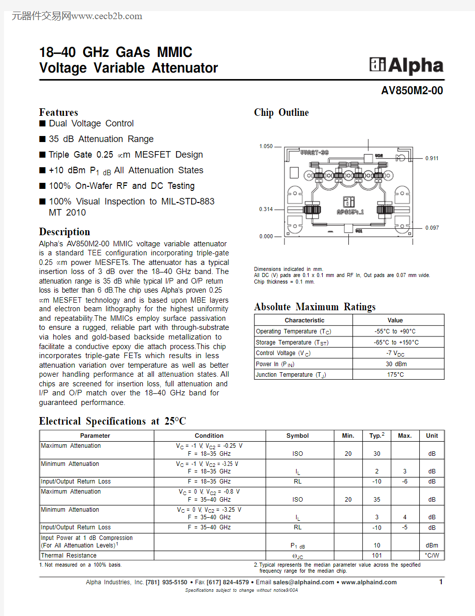
Chip Outline
AV850M2-00
Description
Alpha’s AV850M2-00 MMIC voltage variable attenuator is a standard TEE configuration incorporating triple-gate 0.25 μm power MESFETs.The attenuator has a typical insertion loss of 3 dB over the 18–40 GHz band.The attenuation range is 35 dB while typical I/P and O/P return loss is better than 6 dB.The chip uses Alpha’s proven 0.25μm MESFET technology and is based upon MBE layers and electron beam lithography for the highest uniformity and repeatability.The MMICs employ surface passivation to ensure a rugged, reliable part with through-substrate via holes and gold-based backside metallization to facilitate a conductive epoxy die attach process.This chip incorporates triple-gate FETs which results in less attenuation variation over temperature as well as better power handling performance at all attenuation states.All chips are screened for insertion loss, full attenuation and I/P and O/P match over the 18–40 GHz band for guaranteed performance.
Parameter
Condition
Symbol Min.Typ.2Max.Unit Maximum Attenuation V C = -1 V , V C2= -0.25 V
F = 18–35 GHz ISO 20
30dB
Minimum Attenuation V C = -1 V , V C2= -3.25 V
F = 18–35 GHz
I L 23dB Input/Output Return Loss F = 18–35 GHz RL -10
-6
dB Maximum Attenuation V C = 0 V , V C2= -0.8 V F = 35–40 GHz ISO 2035dB
Minimum Attenuation V C = 0 V , V C2= -3.25 V
F = 35–40 GHz
I L 34dB Input/Output Return Loss
F = 35–40 GHz
RL -10-5
dB Input Power at 1 dB Compression (For All Attenuation Levels)1P 1 dB 10dBm Thermal Resistance
ΘJC
101
°C/W
Electrical Specifications at 25°C
0.000
0.000
0.314
0.750
0.097
1.500
0.982
0.911
1.050
Dimensions indicated in mm.
All DC (V) pads are 0.1 x 0.1 mm and RF In, Out pads are 0.07 mm wide.Chip thickness = 0.1 mm.
Characteristic
Value Operating T emperature (T C )-55°C to +90°C Storage T emperature (T ST )-65°C to +150°C
Control Voltage (V C )-7
V DC Power In (P IN )
30 dBm Junction T emperature (T J )
175°C
Absolute Maximum Ratings
1.Not measured on a 100% basis.
2.Typical represents the median parameter value across the specified frequency range for the median chip.
18–40 GHz GaAs MMIC Voltage Variable Attenuator
AV850M2-00
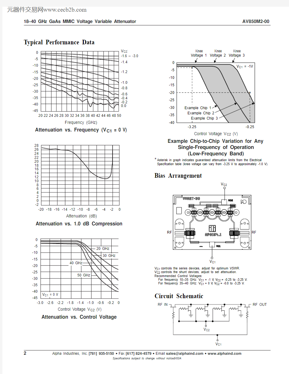
Attenuation vs. Frequency (V C1 = 0 V)
Frequency (GHz)
-45
-35-4020222426283036384032344648424450
-30-25-20-15-10-5A t t e n u a t i o n (d B )
0-0.20.0
-0.4-0.6-0.8-1.0-1.2-1.4-1.6 – -3.0V C2
:
Example Chip-to-Chip Variation for Any
Single-Frequency of Operation
(Low-Frequency Band)
Control Voltage V C2 (V)
A t t e n u a t i o n (d
B )
-40
-35-30-25-20-15-10-5
0-3.25
-0.25
Knee
Knee Knee Attenuation vs. 1.0 dB Compression
Attenuation (dB)
1086420-2
-20-18-16-14-12-10-8
-6-4-20
1214161820222426I n p u t P
o w e r a t 1 d B
28Attenuation vs. Control Voltage
Control Voltage V C2 (V)
-3.0-2.6-2.2-1.8-1.4-0.6-0.2-1.00
A t t e n u a t i o n (d
B )
-45
-35-40
-30-25-20-15-10-5
Typical Performance Data
C1
Bias Arrangement
C1
RF OUT
RF IN
Circuit Schematic
V C1controls the series devices, adjust for optimum VSWR.V C2controls the shunt devices, adjust to set attenuation.Recommended Control Voltages:
For frequency 18–35 GHz:V C1= -1 V , V C2= -0.25 to -3.25 V .For frequency 35–40 GHz:V C1= 0 V , V C2= -0.8 to -3.25 V .
*Asterisk in graph indicates guaranteed attenuation limits from the Electrical
Specification table (knee voltage can vary from -3.25 V to approximately -1.0 V).