SN74LVC374ADBLE中文资料

https://www.360docs.net/doc/075709055.html,
FEATURES
12345678910
20191817161514131211
OE 1Q 1D 2D 2Q 3Q 3D 4D 4Q GND
V CC 8Q 8D 7D 7Q 6Q 6D 5D 5Q CLK
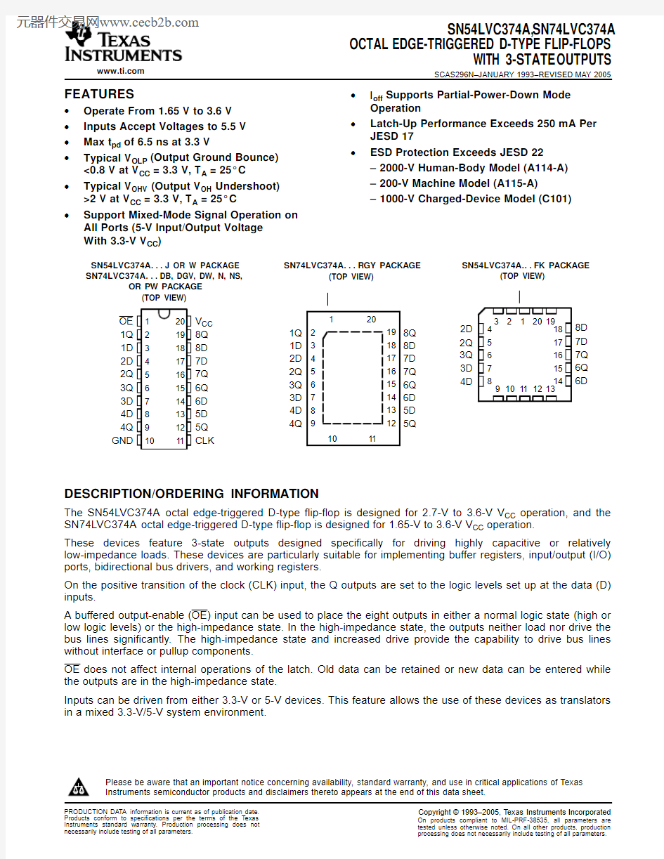
SN54LVC374A...J OR W PACKAGE SN74LVC374A...DB, DGV, DW, N, NS,
OR PW PACKAGE
(TOP VIEW)
SN54LVC374A...FK PACKAGE
(TOP VIEW)
3212019
910111213
45678
18
1716
1514
1D 1Q O E 5Q 5D
8Q
4Q G N D C L K V C C
8D 7D 7Q 6Q 6D
SN74LVC374A...RGY PACKAGE
(TOP VIEW)120
10
11
23456789
19181716151413128Q 8D 7D 7Q 6Q 6D 5D 5Q
1Q 1D 2D 2Q 3Q 3D 4D 4Q
C L K
V G N D
C C
O E
2D 2Q 3Q 3D 4D
DESCRIPTION/ORDERING INFORMATION
SN54LVC374A,SN74LVC374A
OCTAL EDGE-TRIGGERED D-TYPE FLIP-FLOPS
WITH 3-STATE OUTPUTS
SCAS296N–JANUARY 1993–REVISED MAY 2005
?I off Supports Partial-Power-Down Mode Operation
?Operate From 1.65V to 3.6V ?Latch-Up Performance Exceeds 250mA Per ?Inputs Accept Voltages to 5.5V JESD 17
?Max t pd of 6.5ns at 3.3V
?
ESD Protection Exceeds JESD 22
?Typical V OLP (Output Ground Bounce)–2000-V Human-Body Model (A114-A)<0.8V at V CC =3.3V,T A =25°C
–200-V Machine Model (A115-A)
?Typical V OHV (Output V OH Undershoot)>2V at V CC =3.3V,T A =25°C
–1000-V Charged-Device Model (C101)
?
Support Mixed-Mode Signal Operation on All Ports (5-V Input/Output Voltage With 3.3-V V CC )
The SN54LVC374A octal edge-triggered D-type flip-flop is designed for 2.7-V to 3.6-V V CC operation,and the SN74LVC374A octal edge-triggered D-type flip-flop is designed for 1.65-V to 3.6-V V CC operation.
These devices feature 3-state outputs designed specifically for driving highly capacitive or relatively low-impedance loads.These devices are particularly suitable for implementing buffer registers,input/output (I/O)ports,bidirectional bus drivers,and working registers.
On the positive transition of the clock (CLK)input,the Q outputs are set to the logic levels set up at the data (D)inputs.
A buffered output-enable (OE)input can be used to place the eight outputs in either a normal logic state (high or low logic levels)or the high-impedance state.In the high-impedance state,the outputs neither load nor drive the bus lines significantly.The high-impedance state and increased drive provide the capability to drive bus lines without interface or pullup components.
OE does not affect internal operations of the latch.Old data can be retained or new data can be entered while the outputs are in the high-impedance state.
Inputs can be driven from either 3.3-V or 5-V devices.This feature allows the use of these devices as translators in a mixed 3.3-V/5-V system environment.
Please be aware that an important notice concerning availability,standard warranty,and use in critical applications of Texas Instruments semiconductor products and disclaimers thereto appears at the end of this data sheet.
元器件交易网https://www.360docs.net/doc/075709055.html,
https://www.360docs.net/doc/075709055.html,
DESCRIPTION/ORDERING INFORMATION (CONTINUED)
OE
To Seven Other Channels
CLK
1D
1Q
SN54LVC374A,SN74LVC374A
OCTAL EDGE-TRIGGERED D-TYPE FLIP-FLOPS
WITH 3-STATE OUTPUTS
SCAS296N–JANUARY 1993–REVISED MAY 2005
These devices are fully specified for partial-power-down applications using I off .The I off circuitry disables the outputs,preventing damaging current backflow through the devices when they are powered down.
To ensure the high-impedance state during power up or power down,OE should be tied to V CC through a pullup resistor;the minimum value of the resistor is determined by the current-sinking capability of the driver.
ORDERING INFORMATION
T A
PACKAGE (1)
ORDERABLE PART NUMBER TOP-SIDE MARKING PDIP –N Tube of 20SN74LVC374AN SN74LVC374AN QFN –RGY Reel of 1000SN74LVC374ARGYR LC374A Tube of 25SN74LVC374ADW SOIC –DW
LVC374A Reel of 2000SN74LVC374ADWR SOP –NS Reel of 2000SN74LVC374ANSR LVC374A –40°C to 85°C
SSOP –DB Reel of 2000SN74LVC374ADBR LC374A
Tube of 70SN74LVC374APW TSSOP –PW Reel of 2000SN74LVC374APWR LC374A
Reel of 250SN74LVC374APWT TVSOP –DGV Reel of 2000SN74LVC374ADGVR LC374A
CDIP –J
Tube of 20SNJ54LVC374AJ SNJ54LVC374AJ –55°C to 125°C
CFP –W Tube of 85SNJ54LVC374AW SNJ54LVC374AW LCCC –FK
Tube of 55
SNJ54LVC374AFK
SNJ54LVC374AFK (1)
Package drawings,standard packing quantities,thermal data,symbolization,and PCB design guidelines are available at https://www.360docs.net/doc/075709055.html,/sc/package.
FUNCTION TABLE (EACH FLIP-FLOP)
INPUTS
OUTPUT
Q
OE CLK D L ↑H H L ↑L L L H or L X Q 0H
X
X
Z
LOGIC DIAGRAM (POSITIVE LOGIC)
元器件交易网https://www.360docs.net/doc/075709055.html,
https://www.360docs.net/doc/075709055.html,
Absolute Maximum Ratings(1)
SN54LVC374A,SN74LVC374A OCTAL EDGE-TRIGGERED D-TYPE FLIP-FLOPS
WITH3-STATE OUTPUTS
SCAS296N–JANUARY1993–REVISED MAY2005
over operating free-air temperature range(unless otherwise noted)
MIN MAX UNIT V CC Supply voltage range–0.5 6.5V
V I Input voltage range(2)–0.5 6.5V
V O Voltage range applied to any output in the high-impedance or power-off state(2)(3)–0.5 6.5V
V O Voltage range applied to any output in the high or low state–0.5V CC+0.5V
I IK Input clamp current V I<0–50mA
I OK Output clamp current V O<0–50mA
I O Continuous output current±50mA
Continuous current through V CC or GND±100mA
DB package(4)70
DGV package(4)92
DW package(4)58θJA Package thermal impedance N package(4)69°C/W
NS package(4)60
PW package(4)83
RGY package(5)37 T stg Storage temperature range–65150°C
(1)Stresses beyond those listed under"absolute maximum ratings"may cause permanent damage to the device.These are stress ratings
only,and functional operation of the device at these or any other conditions beyond those indicated under"recommended operating
conditions"is not implied.Exposure to absolute-maximum-rated conditions for extended periods may affect device reliability.
(2)The input negative-voltage and output voltage ratings may be exceeded if the input and output current ratings are observed.
(3)The value of V CC is provided in the recommended operating conditions table.
(4)The package thermal impedance is calculated in accordance with JESD51-7.
(5)The package thermal impedance is calculated in accordance with JESD51-5.
元器件交易网https://www.360docs.net/doc/075709055.html,
https://www.360docs.net/doc/075709055.html,
Recommended Operating Conditions (1)
SN54LVC374A,SN74LVC374A
OCTAL EDGE-TRIGGERED D-TYPE FLIP-FLOPS
WITH 3-STATE OUTPUTS
SCAS296N–JANUARY 1993–REVISED MAY 2005
SN54LVC374A
SN74LVC374A UNIT MIN
MAX MIN MAX Operating
2 3.6
1.65 3.6
V CC
Supply voltage
V
Data retention only 1.5
1.5
V CC =1.65V to 1.95V
0.65×V CC
V IH
High-level input voltage
V CC =2.3V to 2.7V 1.7V
V CC =2.7V to 3.6V 22
V CC =1.65V to 1.95V
0.35×V CC
V IL Low-level input voltage V CC =2.3V to 2.7V 0.7V V CC =2.7V to 3.6V
0.80.8V I Input voltage 0 5.50 5.5V High or low state 0V CC 0V CC V O
Output voltage
V 3-state 0
5.5
5.5V CC =1.65V
–4V CC =2.3V –8I OH
High-level output current
mA V CC =2.7V –12–12V CC =3V –24
–24V CC =1.65V
4V CC =2.3V 8I OL
Low-level output current
mA V CC =2.7V 1212V CC =3V
2424?t/?v Input transition rise or fall rate 1010ns/V T A Operating free-air temperature
–55
125
–40
85
°C (1)
All unused inputs of the device must be held at V CC or GND to ensure proper device operation.Refer to the TI application report,Implications of Slow or Floating CMOS Inputs ,literature number SCBA004.
元器件交易网https://www.360docs.net/doc/075709055.html,
https://www.360docs.net/doc/075709055.html,
Electrical Characteristics
SN54LVC374A,SN74LVC374A OCTAL EDGE-TRIGGERED D-TYPE FLIP-FLOPS
WITH3-STATE OUTPUTS
SCAS296N–JANUARY1993–REVISED MAY2005
over recommended operating free-air temperature range(unless otherwise noted)
SN54LVC374A SN74LVC374A PARAMETER TEST CONDITIONS V CC UNIT
MIN TYP(1)MAX MIN TYP(1)MAX
1.65V to3.6V V CC–0.2
I OH=–100μA
2.7V to
3.6V V CC–0.2
I OH=–4mA 1.65V 1.2
V OH I OH=–8mA 2.3V 1.7V
2.7V 2.2 2.2
I OH=–12mA
3V 2.4 2.4
I OH=–24mA3V 2.2 2.2
1.65V to3.6V0.2
I OL=100μA
2.7V to
3.6V0.2
I OL=4mA 1.65V0.45
V OL V
I OL=8mA 2.3V0.7
I OL=12mA 2.7V0.40.4
I OL=24mA3V0.550.55
I I V I=0to5.5V 3.6V±5±5μA
I off V I or V O=5.5V0±10μA
I OZ V O=0to5.5V 3.6V±15±10μA
V I=V CC or GND1010
I CC I O=0 3.6VμA
3.6V≤V I≤5.5V(2)1010
One input at V CC–0.6V,
?I CC 2.7V to3.6V500500μA Other inputs at V CC or GND
C i V I=V CC or GN
D 3.3V4124pF
C o V O=V CC or GN
D 3.3V 5.512 5.5pF
(1)All typical values are at V CC=3.3V,T A=25°C.
(2)This applies in the disabled state only.
元器件交易网https://www.360docs.net/doc/075709055.html,
https://www.360docs.net/doc/075709055.html,
Timing Requirements
Timing Requirements
Switching Characteristics
Switching Characteristics
SN54LVC374A,SN74LVC374A
OCTAL EDGE-TRIGGERED D-TYPE FLIP-FLOPS
WITH 3-STATE OUTPUTS
SCAS296N–JANUARY 1993–REVISED MAY 2005
over recommended operating free-air temperature range (unless otherwise noted)(see Figure 1)
SN54LVC374A V CC =3.3V V CC =2.7V UNIT
±0.3V MIN
MAX MIN
MAX f clock Clock frequency
80
100
MHz t w Pulse duration,CLK high or low 3.3 3.3ns t su Setup time,data before CLK ↑22ns t h
Hold time,data after CLK ↑
1.5
1.5ns over recommended operating free-air temperature range (unless otherwise noted)(see Figure 1)
SN74LVC374A
V CC =1.8V V CC =2.5V V CC =3.3V V CC =2.7V UNIT
±0.15V ±0.2V ±0.3V MIN
MAX
MIN
MAX
MIN MAX MIN MAX f clock Clock frequency
(1)
(1)
80
100
MHz t w Pulse duration,CLK high or low (1)(1) 3.3 3.3ns t su Setup time,data before CLK ↑(1)(1)22ns t h Hold time,data after CLK ↑
(1)
(1)
1.5
1.5
ns
(1)
This information was not available at the time of publication.
over recommended operating free-air temperature range (unless otherwise noted)(see Figure 1)
SN54LVC374A
FROM TO V CC =3.3V PARAMETER
V CC =2.7V UNIT
(INPUT)
(OUTPUT)
±0.3V MIN
MAX
MIN MAX
f max 80
100MHz t pd CLK Q 9.518.5ns t en OE Q 9.518.5ns t dis
OE
Q
81
7ns over recommended operating free-air temperature range (unless otherwise noted)(see Figure 1)
SN74LVC374A
FROM TO V CC =1.8V V CC =2.5V V CC =3.3V PARAMETER
V CC =2.7V UNIT
(INPUT)
(OUTPUT)
±0.15V ±0.2V ±0.3V MIN
MAX MIN
MAX
MIN MAX
MIN MAX
f max (1)(1)80
100MHz t pd CLK Q (1)(1)(1)(1)8.1 1.57ns t en OE Q (1)(1)(1)(1)8.5 1.57.5ns t dis OE
Q
(1)
(1)
(1)
(1)
7.1 1.5
6.5ns t sk(o)
1ns
(1)
This information was not available at the time of publication.
元器件交易网https://www.360docs.net/doc/075709055.html,
https://www.360docs.net/doc/075709055.html,
Operating Characteristics
SN54LVC374A,SN74LVC374A OCTAL EDGE-TRIGGERED D-TYPE FLIP-FLOPS
WITH3-STATE OUTPUTS
SCAS296N–JANUARY1993–REVISED MAY2005
T
A
=25°C
V CC=1.8V V CC=2.5V V CC=3.3V
TEST
PARAMETER UNIT
CONDITIONS TYP TYP TYP
Outputs enabled(1)(1)54.5 Power dissipation capacitance
C pd f=10MHz pF
per flip-flop Outputs disabled(1)(1)13.5
(1)This information was not available at the time of publication.
元器件交易网https://www.360docs.net/doc/075709055.html,
https://www.360docs.net/doc/075709055.html,
PARAMETER MEASUREMENT INFORMATION
From Output Under Test
LOAD CIRCUIT
Open Data Input
Timing Input
V I
0 V
V I
0 V
0 V
Input
VOLTAGE WAVEFORMS SETUP AND HOLD TIMES
VOLTAGE WAVEFORMS PROPAGATION DELAY TIMES
INVERTING AND NONINVERTING OUTPUTS
VOLTAGE WAVEFORMS PULSE DURATION
V OH
V OH
V OL
V OL
V I
0 V Input
Output Waveform 1S1 at V LOAD (see Note B)
Output Waveform 2S1 at GND (see Note B)
V OL
V OH V LOAD /2
0 V
≈0 V
V I
VOLTAGE WAVEFORMS ENABLE AND DISABLE TIMES LOW- AND HIGH-LEVEL ENABLING
Output
Output
t PLH /t PHL t PLZ /t PZL t PHZ /t PZH
Open V LOAD GND
TEST S1NOTES: A.C L includes probe and jig capacitance.
B.Waveform 1 is for an output with internal conditions such that the output is low except when disabled by the output control.
Waveform 2 is for an output with internal conditions such that the output is high except when disabled by the output control.C.All input pulses are supplied by generators having the following characteristics: PRR ≤ 10 MHz, Z O = 50 ?.D.The outputs are measured one at a time with one transition per measurement.E.t PLZ and t PHZ are the same as t dis .F.t PZL and t PZH are the same as t en .G.t PLH and t PHL are the same as t pd .
H.All parameters and waveforms are not applicable to all devices.
Output Control V I
1.8 V ± 0.15 V
2.5 V ± 0.2 V
2.7 V
3.3 V ± 0.3 V
1 k ?500 ?500 ?500 ?
V CC R L 2 × V CC 2 × V CC 6 V 6 V
V LOAD C L 30 pF 30 pF 50 pF 50 pF
0.15 V 0.15 V 0.3 V 0.3 V
V ?V CC V CC 2.7 V 2.7 V
V I V CC /2V CC /21.5 V 1.5 V
V M t r /t f ≤2 ns ≤2 ns ≤2.5 ns ≤2.5 ns
INPUTS SN54LVC374A,SN74LVC374A
OCTAL EDGE-TRIGGERED D-TYPE FLIP-FLOPS
WITH 3-STATE OUTPUTS
SCAS296N–JANUARY 1993–REVISED MAY 2005
Figure 1.Load Circuit and Voltage Waveforms
元器件交易网https://www.360docs.net/doc/075709055.html,
PACKAGING INFORMATION
Orderable Device Status(1)Package
Type Package
Drawing
Pins Package
Qty
Eco Plan(2)Lead/Ball Finish MSL Peak Temp(3)
5962-9757401Q2A ACTIVE LCCC FK201TBD Call TI Level-NC-NC-NC 5962-9757401QRA ACTIVE CDIP J201TBD Call TI Level-NC-NC-NC 5962-9757401QSA ACTIVE CFP W201TBD Call TI Level-NC-NC-NC 5962-9757401VRA ACTIVE CDIP J201TBD Call TI Level-NC-NC-NC 5962-9757401VSA ACTIVE CFP W201TBD Call TI Level-NC-NC-NC
SN74LVC374ADBLE OBSOLETE SSOP DB20TBD Call TI Call TI
SN74LVC374ADBR ACTIVE SSOP DB202000Green(RoHS&
no Sb/Br)
CU NIPDAU Level-1-260C-UNLIM
SN74LVC374ADBRE4ACTIVE SSOP DB202000Green(RoHS&
no Sb/Br)
CU NIPDAU Level-1-260C-UNLIM
SN74LVC374ADGVR ACTIVE TVSOP DGV202000Green(RoHS&
no Sb/Br)
CU NIPDAU Level-1-260C-UNLIM
SN74LVC374ADGVRE4ACTIVE TVSOP DGV202000Green(RoHS&
no Sb/Br)
CU NIPDAU Level-1-260C-UNLIM
SN74LVC374ADW ACTIVE SOIC DW2025Green(RoHS&
no Sb/Br)
CU NIPDAU Level-1-260C-UNLIM
SN74LVC374ADWE4ACTIVE SOIC DW2025Green(RoHS&
no Sb/Br)
CU NIPDAU Level-1-260C-UNLIM
SN74LVC374ADWR ACTIVE SOIC DW202000Green(RoHS&
no Sb/Br)
CU NIPDAU Level-1-260C-UNLIM
SN74LVC374ADWRE4ACTIVE SOIC DW202000Green(RoHS&
no Sb/Br)
CU NIPDAU Level-1-260C-UNLIM
SN74LVC374AN ACTIVE PDIP N2020Pb-Free
(RoHS)
CU NIPDAU Level-NC-NC-NC
SN74LVC374ANE4ACTIVE PDIP N2020Pb-Free
(RoHS)
CU NIPDAU Level-NC-NC-NC
SN74LVC374ANSR ACTIVE SO NS202000Green(RoHS&
no Sb/Br)
CU NIPDAU Level-1-260C-UNLIM
SN74LVC374ANSRE4ACTIVE SO NS202000Green(RoHS&
no Sb/Br)
CU NIPDAU Level-1-260C-UNLIM
SN74LVC374APW ACTIVE TSSOP PW2070Green(RoHS&
no Sb/Br)
CU NIPDAU Level-1-260C-UNLIM
SN74LVC374APWE4ACTIVE TSSOP PW2070Green(RoHS&
no Sb/Br)
CU NIPDAU Level-1-260C-UNLIM SN74LVC374APWLE OBSOLETE TSSOP PW20TBD Call TI Call TI
SN74LVC374APWR ACTIVE TSSOP PW202000Green(RoHS&
no Sb/Br)
CU NIPDAU Level-1-260C-UNLIM
SN74LVC374APWRE4ACTIVE TSSOP PW202000Green(RoHS&
no Sb/Br)
CU NIPDAU Level-1-260C-UNLIM
SN74LVC374APWRG4ACTIVE TSSOP PW202000Green(RoHS&
no Sb/Br)
CU NIPDAU Level-1-260C-UNLIM
SN74LVC374APWT ACTIVE TSSOP PW20250Green(RoHS&
no Sb/Br)
CU NIPDAU Level-1-260C-UNLIM
SN74LVC374APWTE4ACTIVE TSSOP PW20250Green(RoHS&
no Sb/Br)
CU NIPDAU Level-1-260C-UNLIM
SN74LVC374ARGYR ACTIVE QFN RGY201000Green(RoHS&
no Sb/Br)
CU NIPDAU Level-2-260C-1YEAR SNJ54LVC374AFK ACTIVE LCCC FK201TBD Call TI Level-NC-NC-NC
Orderable Device Status(1)Package
Type Package
Drawing
Pins Package
Qty
Eco Plan(2)Lead/Ball Finish MSL Peak Temp(3)
SNJ54LVC374AJ ACTIVE CDIP J201TBD Call TI Level-NC-NC-NC SNJ54LVC374AW ACTIVE CFP W201TBD Call TI Level-NC-NC-NC
(1)The marketing status values are defined as follows:
ACTIVE:Product device recommended for new designs.
LIFEBUY:TI has announced that the device will be discontinued,and a lifetime-buy period is in effect.
NRND:Not recommended for new designs.Device is in production to support existing customers,but TI does not recommend using this part in a new design.
PREVIEW:Device has been announced but is not in production.Samples may or may not be available.
OBSOLETE:TI has discontinued the production of the device.
(2)Eco Plan-The planned eco-friendly classification:Pb-Free(RoHS)or Green(RoHS&no Sb/Br)-please check https://www.360docs.net/doc/075709055.html,/productcontent for the latest availability information and additional product content details.
TBD:The Pb-Free/Green conversion plan has not been defined.
Pb-Free(RoHS):TI's terms"Lead-Free"or"Pb-Free"mean semiconductor products that are compatible with the current RoHS requirements for all6substances,including the requirement that lead not exceed0.1%by weight in homogeneous materials.Where designed to be soldered at high temperatures,TI Pb-Free products are suitable for use in specified lead-free processes.
Green(RoHS&no Sb/Br):TI defines"Green"to mean Pb-Free(RoHS compatible),and free of Bromine(Br)and Antimony(Sb)based flame retardants(Br or Sb do not exceed0.1%by weight in homogeneous material)
(3)MSL,Peak Temp.--The Moisture Sensitivity Level rating according to the JEDEC industry standard classifications,and peak solder temperature.
Important Information and Disclaimer:The information provided on this page represents TI's knowledge and belief as of the date that it is provided.TI bases its knowledge and belief on information provided by third parties,and makes no representation or warranty as to the accuracy of such information.Efforts are underway to better integrate information from third parties.TI has taken and continues to take reasonable steps to provide representative and accurate information but may not have conducted destructive testing or chemical analysis on incoming materials and chemicals.TI and TI suppliers consider certain information to be proprietary,and thus CAS numbers and other limited information may not be available for release.
In no event shall TI's liability arising out of such information exceed the total purchase price of the TI part(s)at issue in this document sold by TI to Customer on an annual basis.
元器件交易网https://www.360docs.net/doc/075709055.html,