LTC2227CUH#PBF;LTC2226IUH#PBF;LTC2228CUH#PBF;LTC2228IUH#PBF;LTC2227IUH#PBF;中文规格书,Datasheet资料

1
222876fb
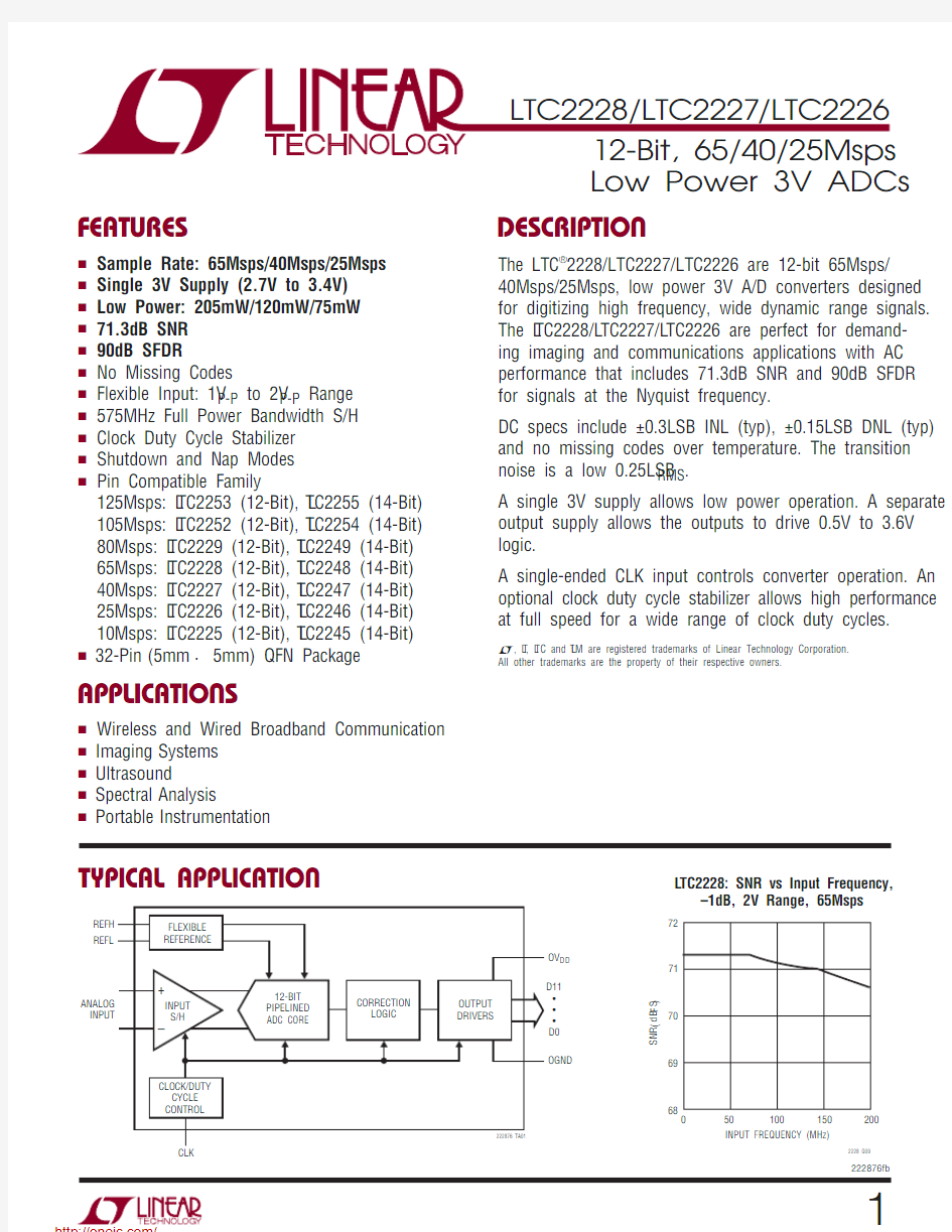
T YPICAL APPLICATION
F EATURES
A PPLICATIONS
D ESCRIPTION Low Power 3V ADCs
The LTC ?2228/LTC2227/LTC2226 are 12-bit 65Msps/
40Msps/25Msps, low power 3V A/D converters designed for digitizing high frequency, wide dynamic range signals. The L TC2228/L TC2227/L TC2226 are perfect for demand-ing imaging and communications applications with AC performance that includes 71.3dB SNR and 90dB SFDR for signals at the Nyquist frequency.
DC specs include ±0.3LSB INL (typ), ±0.15LSB DNL (typ) and no missing codes over temperature. The transition noise is a low 0.25LSB RMS .
A single 3V supply allows low power operation. A separate output supply allows the outputs to drive 0.5V to 3.6V logic.
A single-ended CLK input controls converter operation. An optional clock duty cycle stabilizer allows high performance at full speed for a wide range of clock duty cycles.
L TC2228: SNR vs Input Frequency,
–1dB, 2V Range, 65Msps
n
Sample Rate: 65Msps/40Msps/25Msps n Single 3V Supply (2.7V to 3.4V)n Low Power: 205mW/120mW/75mW n 71.3dB SNR n 90dB SFDR
n No Missing Codes n Flexible Input: 1V P-P to 2V P-P Range n 575MHz Full Power Bandwidth S/H n Clock Duty Cycle Stabilizer n Shutdown and Nap Modes n Pin Compatible Family
125Msps: L TC2253 (12-Bit), L TC2255 (14-Bit) 105Msps: L TC2252 (12-Bit), L TC2254 (14-Bit) 80Msps: L TC2229 (12-Bit), L TC2249 (14-Bit) 65Msps: L TC2228 (12-Bit), L TC2248 (14-Bit) 40Msps: L TC2227 (12-Bit), L TC2247 (14-Bit) 25Msps: L TC2226 (12-Bit), L TC2246 (14-Bit) 10Msps: L TC2225 (12-Bit), L TC2245 (14-Bit)n 32-Pin (5mm × 5mm) QFN Package
n
Wireless and Wired Broadband Communication n Imaging Systems n Ultrasound n Spectral Analysis n Portable Instrumentation
L , L T , L TC and L TM are registered trademarks of Linear Technology Corporation.
All other trademarks are the property of their respective owners.
???D0REFL
DD
INPUT FREQUENCY (MHz)
S N R (d B F S )
70
71200
2228 G09
69
68
50
10015072
https://www.360docs.net/doc/006647333.html,/
LTC2228/LTC2227/LTC22262
222876fb
P IN CONFIGURATION
A BSOLUTE MAXIMUM RATINGS Supply Voltage (V DD ) ..................................................4V Digital Output Ground Voltage (OGND) ........–0.3V to 1V Analog Input Voltage (Note 3) .......–0.3V to (V DD + 0.3V)Digital Input Voltage ......................–0.3V to (V DD + 0.3V)Digital Output Voltage ................–0.3V to (OV DD + 0.3V)Power Dissipation .............................................1500mW Operating Temperature Range
L TC2228C, L TC2227C, L TC2226C.............0°C to 70°C L TC2228I, L TC2227I, L TC2226I ............–40°C to 85°C Storage Temperature Range ...................–65°C to 125°C
OV DD = V DD (Notes 1, 2)
3231302928272625
9101112TOP VIEW UH PACKAGE
32-LEAD (5mm s 5mm) PLASTIC QFN
13141516
17181920212223248
7654321
A IN +A IN –REFH REFH REFL REFL V DD GND D8D7D6
OV DD OGND D5D4D3
V D D
V C M
S E N S E
M O D E
O F
D 11
D 10D 9
C L K
S H D N
O E
N C
N C
D 0
D 1
D 2
33
T JMAX = 125°C, θJA = 34°C/W
EXPOSED PAD (PIN 33) IS GND, MUST BE SOLDERED TO PCB
ORDER INFORMATION
LEAD FREE FINISH TAPE AND REEL PART MARKING*PACKAGE DESCRIPTION
TEMPERATURE RANGE L TC2228CUH#PBF L TC2228CUH#TRPBF 222832-Lead (5mm × 5mm) Plastic QFN 0°C to 70°C L TC2228IUH#PBF L TC2228IUH#TRPBF 222832-Lead (5mm × 5mm) Plastic QFN –40°C to 85°C L TC2227CUH#PBF L TC2227CUH#TRPBF 222732-Lead (5mm × 5mm) Plastic QFN 0°C to 70°C L TC2227IUH#PBF L TC2227IUH#TRPBF 222732-Lead (5mm × 5mm) Plastic QFN –40°C to 85°C L TC2226CUH#PBF L TC2226CUH#TRPBF 222632-Lead (5mm × 5mm) Plastic QFN 0°C to 70°C L TC2226IUH#PBF L TC2226IUH#TRPBF 2226
32-Lead (5mm × 5mm) Plastic QFN –40°C to 85°C LEAD BASED FINISH TAPE AND REEL PART MARKING*PACKAGE DESCRIPTION
TEMPERATURE RANGE L TC2228CUH L TC2228CUH#TR 222832-Lead (5mm × 5mm) Plastic QFN 0°C to 70°C L TC2228IUH L TC2228IUH#TR 222832-Lead (5mm × 5mm) Plastic QFN –40°C to 85°C L TC2227CUH L TC2227CUH#TR 222732-Lead (5mm × 5mm) Plastic QFN 0°C to 70°C L TC2227IUH L TC2227IUH#TR 222732-Lead (5mm × 5mm) Plastic QFN –40°C to 85°C L TC2226CUH L TC2226CUH#TR 222632-Lead (5mm × 5mm) Plastic QFN 0°C to 70°C L TC2226IUH
L TC2226IUH#TR
2226
32-Lead (5mm × 5mm) Plastic QFN
–40°C to 85°C
Consult L TC Marketing for parts speci? ed with wider operating temperature ranges. *The temperature grade is identi? ed by a label on the shipping container .For more information on lead free part marking, go to: http://www.linear .com/leadfree/ For more information on tape and reel speci? cations, go to: http://www.linear .com/tapeandreel/
https://www.360docs.net/doc/006647333.html,/
LTC2228/LTC2227/LTC2226
3
222876fb
CONVERTER CHARACTERISTICS The l denotes the speci? cations which apply over the full operating
temperature range, otherwise speci? cations are at T A = 25°C. (Note 4)
PARAMETER CONDITIONS
L TC2228L TC2227
L TC2226
UNITS MIN TYP MAX MIN TYP MAX MIN TYP MAX Resolution
(No Missing Codes)l
121212Bits Integral
Linearity Error Differential Analog Input (Note 5)l –1.1±0.3 1.1–1±0.31–1±0.31LSB Differential Linearity Error Differential Analog Input l –0.8±0.150.8–0.7±0.150.7–0.7±0.150.7LSB Offset Error (Note 6)l –12±212–12±212–12±212mV Gain Error External Reference l
–2.5
±0.5 2.5
–2.5
±0.5 2.5
–2.5
±0.5 2.5
%FS Offset Drift ±10±10±10μV/°C Full-Scale Drift Internal Reference ±30±30±30ppm/°C External Reference ±5±5±5ppm/°C T ransition Noise
SENSE = 1V
0.25
0.25
0.25
LSB RMS
ANALOG INPUT The l denotes the speci? cations which apply over the full operating temperature range, otherwise
speci? cations are at T A = 25°C. (Note 4)
SYMBOL PARAMETER
CONDITIONS
MIN TYP MAX UNITS
V IN Analog Input Range (A IN + – A IN –)
2.7V < V DD <
3.4V (Note 7)l ±0.5V to ±1V
V V IN,CM Analog Input Common Mode (A IN + + A IN –)/2Differential Input (Note 7)
Single-Ended Input (Note 7)l l 10.5 1.51.5
1.92V V I IN Analog Input Leakage Current 0V < A IN +, A IN – < V DD l –11μA I SENSE SENSE Input Leakage 0V < SENSE < 1V
l –33μA I MODE MODE Pin Leakage
l
–3
3
μA t AP Sample-and-Hold Acquisition Delay Time 0ns t JITTER Sample-and-Hold Acquisition Delay Time Jitter 0.2ps RMS
CMRR
Analog Input Common Mode Rejection Ratio 80dB Full Power Bandwidth
Figure 8 Test Circuit
575
MHz
DYNAMIC ACCURACY The l denotes the speci? cations which apply over the full operating temperature range,
otherwise speci? cations are at T A = 25°C. A IN = –1dBFS. (Note 4)
SYMBOL PARAMETER CONDITIONS
L TC2228
L TC2227
L TC2226
UNITS MIN
TYP MAX MIN
TYP MAX MIN TYP MAX SNR
Signal-to-Noise Ratio 5MHz Input
71.3
71.4
71.4dB 12.5MHz Input l 70.2
71.2
dB 20MHz Input l 70.1
71.3dB 30MHz Input l
70
71.3dB 70MHz Input 71.371.170.9dB 140MHz Input
7170.770.6dB SFDR
Spurious Free Dynamic Range 2nd or 3rd
Harmonic
5MHz Input 90
90
90dB 12.5MHz Input l 76
90
dB 20MHz Input l 76
90dB 30MHz Input l
75
90dB 70MHz Input 858585dB 140MHz Input
80
80
80dB
https://www.360docs.net/doc/006647333.html,/
LTC2228/LTC2227/LTC2226
4
222876fb
DYNAMIC ACCURACY The l denotes the speci? cations which apply over the full operating temperature range,
otherwise speci? cations are at T A = 25°C. A IN = –1dBFS. (Note 4)
SYMBOL PARAMETER CONDITIONS L TC2228L TC2227
L TC2226
UNITS MIN
TYP MAX MIN
TYP MAX MIN TYP MAX SFDR
Spurious Free Dynamic Range 4th Harmonic or Higher
5MHz Input
95
95
95dB 12.5MHz Input l 82
95
dB 20MHz Input l 82
95dB 30MHz Input l
82
95dB 70MHz Input 959595dB 140MHz Input 909090dB S/(N+D)
Signal-to-Noise Plus Distortion Ratio
5MHz Input 71.3
71.4
71.4dB 12.5MHz Input l 69.8
71.2
dB 20MHz Input l 69.7
71.2dB 30MHz Input l
69.6
71.2dB 70MHz Input 71.170.970.8dB 140MHz Input 69.969.969.8dB IMD
Intermodulation Distortion
f IN1 = 28.2MHz,f IN2 = 26.8MHz
90
90
90dB
PARAMETER
CONDITIONS MIN TYP MAX UNITS
V CM Output Voltage I OUT = 0
1.475
1.500 1.525
V V CM Output Tempco ±25ppm/°C V CM Line Regulation 2.7V < V DD < 3.4V 3mV/V V CM Output Resistance
–1mA < I OUT < 1mA
4
Ω
INTERNAL REFERENCE CHARACTERISTICS
(Note 4)DIGITAL INPUTS AND DIGITAL OUTPUTS The l denotes the speci? cations which apply over the full
operating temperature range, otherwise speci? cations are at T A = 25°C. (Note 4)
SYMBOL PARAMETER
CONDITIONS MIN TYP MAX UNITS LOGIC INPUTS (CLK, OE , SHDN)
V IH
High Level Input Voltage V DD = 3V
l 2V
V IL
Low Level Input Voltage V DD = 3V l 0.8V I IN
Input Current V IN = 0V to V DD l
–10
10
μA C IN
Input Capacitance (Note 7)
3
pF
LOGIC OUTPUTS OV DD = 3V
C OZ
Hi-Z Output Capacitance OE = High (Note 7)3pF I SOURCE
Output Source Current V OUT = 0V 50mA I SINK
Output Sink Current V OUT = 3V 50mA V OH High Level Output Voltage I O = –10μA I O = –200μA l 2.7
2.9952.99V V V OL
Low Level Output Voltage
I O = 10μA I O = 1.6mA l
0.0050.090.4
V V OV DD = 2.5V
V OH
High Level Output Voltage I O = –200μA 2.49V V OL
Low Level Output Voltage I O = 1.6mA 0.09V OV DD = 1.8V
V OH
High Level Output Voltage I O = –200μA 1.79V V OL
Low Level Output Voltage I O = 1.6mA
0.09
V
https://www.360docs.net/doc/006647333.html,/
LTC2228/LTC2227/LTC2226
5
222876fb
POWER REQUIREMENTS The l denotes the speci? cations which apply over the full operating temperature
range, otherwise speci? cations are at T A = 25°C. (Note 8)
SYMBOL PARAMETER CONDITIONS
L TC2228
L TC2227
L TC2226
UNITS
MIN TYP MAX MIN TYP MAX MIN TYP MAX V DD Analog Supply Voltage (Note 9)l 2.73 3.4 2.73 3.4 2.73 3.4V OV DD Output Supply Voltage (Note 9)l 0.5
3 3.60.5
3 3.60.5
3 3.6V I VDD Supply Current l 68.38040482530mA P DISS Power Dissipation l
205240
120144
7590
mW P SHDN Shutdown Power SHDN = H, OE = H,
No CLK
222mW P NAP
Nap Mode Power
SHDN = H, OE = L, No CLK
15
15
15
mW
TIMING CHARACTERISTICS The l denotes the speci? cations which apply over the full operating temperature
range, otherwise speci? cations are at T A = 25°C. (Note 4)
SYMBOL PARAMETER CONDITIONS L TC2228L TC2227L TC2226UNITS MIN TYP MAX MIN TYP MAX MIN TYP MAX f S Sampling Frequency (Note 9)
l 165140125MHz t L
CLK Low Time
Duty Cycle Stabilizer Off
Duty Cycle Stabilizer On (Note 7)
l l 7.357.77.750050011.8512.5
50050018.952020500500ns ns t H
CLK High Time
Duty Cycle Stabilizer Off Duty Cycle Stabilizer On (Note 7)
l l
7.35
7.77.7500500
11.85
12.512.5500500
18.95
2020500500
ns ns t AP Sample-and-Hold Aperture Delay 0
ns
t D
CLK to DATA Delay C L = 5pF (Note 7)l 1.4 2.7 5.4 1.4 2.7 5.4 1.4 2.7 5.4ns Data Access Time After OE ↓
C L = 5pF (Note 7)l 4.310 4.310 4.310ns BUS Relinquish Time
(Note 7)
l
3.38.5
3.38.5
3.38.5
ns Pipeline Latency
5
5
5
Cycles
Note 1: Stresses beyond those listed under Absolute Maximum Ratings may cause permanent damage to the device. Exposure to any Absolute Maximum Rating condition for extended periods may affect device reliability and lifetime.
Note 2: All voltage values are with respect to ground with GND and OGND wired together (unless otherwise noted).
Note 3: When these pin voltages are taken below GND or above V DD , they will be clamped by internal diodes. This product can handle input currents of greater than 100mA below GND or above V DD without latchup.Note 4: V DD = 3V , f SAMPLE = 65MHz (L TC2228), 40MHz (L TC2227), or 25MHz (L TC2226), input range = 2V P-P with differential drive, unless otherwise noted.
Note 5: Integral nonlinearity is de? ned as the deviation of a code from a straight line passing through the actual endpoints of the transfer curve. The deviation is measured from the center of the quantization band.Note 6: Offset error is the offset voltage measured from –0.5 LSB when the output code ? ickers between 0000 0000 0000 and 1111 1111 1111.Note 7: Guaranteed by design, not subject to test.
Note 8: V DD = 3V , f SAMPLE = 65MHz (L TC2228), 40MHz (L TC2227), or 25MHz (L TC2226), input range = 1V P-P with differential drive.Note 9: Recommend operating conditions.
https://www.360docs.net/doc/006647333.html,/
LTC2228/LTC2227/LTC22266
222876fb
T YPICAL PERFORMANCE CHARACTERISTICS L TC2228: Typical INL, 2V Range,
65Msps
L TC2228: Typical DNL, 2V Range, 65Msps
L TC2228: 8192 Point FFT , f IN = 5MHz, –1dB, 2V Range, 65Msps
L TC2228: 8192 Point FFT ,
f IN = 30MHz, –1dB, 2V Range, 65Msps
L TC2228: 8192 Point 2-Tone FFT ,f IN = 28.2MHz and 26.8MHz, –1dB, 2V Range, 65Msps
L TC2228: Grounded Input Histogram, 65Msps
L TC2228: SNR vs Input Frequency, –1dB, 2V Range, 65Msps
CODE
I N L E R R O R (L S B )
3072
2228 G01
1024
20484096
1.000.750.50
0.250–0.25–0.50–0.75–1.00
CODE
D
N L E R R O R (L S B )
3072
2228 G02
1024
20484096
1.000.750.500.250–0.25–0.50–0.75–1.00
FREQUENCY (MHz)
2228 G03
5
1015A M P L I T U D E
(d B )
202530
0–10–20–30–40–50–60–70–80–90–100–110–120
L TC2228: 8192 Point FFT ,
f IN = 70MHz, –1dB, 2V Range, 65Msps
L TC2228: 8192 Point FFT ,
f IN = 140MHz, –1dB, 2V Range, 65Msps
FREQUENCY (MHz)
2228 G04
5
1015A M P L I T U D E
(
d B )
202530
0–10–20–30–40–50–60–70–80–90–100–110–120
FREQUENCY (MHz)
2228 G05
5
1015A M P L I T U D E
(d B )
202530
0–10–20–30–40
–50–60–70–80–90–100–110–120
FREQUENCY (MHz)
2228 G06
5
1015A M P L I T U D E (d B )
202530
0–10–20–30–40–50–60–70–80–90–100–110
–120
FREQUENCY (MHz)
2228 G07
5
1015A M P L I T U D E (d B )
202530
0–10–20
–30–40
–50–60–70–80–90–100
–110–120
CODE
70000600005000040000300002000010000
20432044
2228 G08
2042
C O U N T
INPUT FREQUENCY (MHz)
S N R (d B F S )
70
71200
2228 G09
69
68
50
10015072
https://www.360docs.net/doc/006647333.html,/
LTC2228/LTC2227/LTC2226
7
222876fb
TYPICAL PERFORMANCE CHARACTERISTICS
L TC2228: SFDR vs Input Frequency, –1dB, 2V Range, 65Msps
L TC2228: SNR and SFDR vs Clock Duty Cycle, 65Msps
L TC2228: SNR vs Input Level, f IN = 30MHz, 2V Range, 65Msps
L TC2228: SFDR vs Input Level, f IN = 30MHz, 2V Range, 65Msps
L TC2228: I VDD vs Sample Rate, 5mHz Sine Wave Input, –1dB
L TC2228: I OVDD vs Sample Rate, 5MHz Sine Wave Input, –1dB, OV DD = 1.8V
L TC2228: SNR and SFDR vs Sample Rate, 2V Range,f IN
= 5MHz, –1dB
INPUT FREQUENCY (MHz)
010095
908580757065
150
2228 G10
50
100200
S F D R (d B F S )
SAMPLE RATE (Msps)
0S N R A N D S F D R (d B F S )
110
100
90
80
70
60
802228 G11
20
40
60100
CLOCK DUTY CYCLE (%)
30
S N R A N D S F D R (d B F S )
60
2228 G12
40
50
70
1009590858075
70
65
35
45
55
65
INPUT LEVEL (dBFS)
–60
–50
S N R (d B c A N D d B F S )
–40–20–30–10
2228 G13
8070
6050
403020100INPUT LEVEL (dBFS)
–60
–50
–40–20–30–100
S F D R (d B c A N D d B F S )
2228 G14
120110100908070605040
30
20SAMPLE RATE (Msps)
0807570
65
605550
602228 G152040805010
3070I V D D (
m A )
SAMPLE RATE (Msps)
I O V D D (m A )
2228 G16
6543210
020405010
30607080
https://www.360docs.net/doc/006647333.html,/
LTC2228/LTC2227/LTC22268
222876fb
T YPICAL PERFORMANCE CHARACTERISTICS L TC2227: Typical INL, 2V Range,
40Msps
L TC2227: Typical DNL, 2V Range, 40Msps
L TC2227: 8192 Point FFT , f IN = 5MHz, –1dB, 2V Range, 40Msps
L TC2228: 8192 Point FFT ,
f IN = 30MHz, –1dB, 2V Range, 40Msps
L TC2227: 8192 Point 2-Tone FFT ,f IN = 21.6MHz and 23.6MHz, –1dB, 2V Range, 40Msps
L TC2227: Grounded Input Histogram, 40Msps
L TC2227: SNR vs Input Frequency, –1dB, 2V Range, 40Msps
L TC2227: 8192 Point FFT ,
f IN = 70MHz, –1dB, 2V Range, 40Msps
L TC2227: 8192 Point FFT ,
f IN = 140MHz, –1dB, 2V Range, 40Msps
CODE
I N L E R R O R (L S B )
3072
2227 G01
1024
20484096
1.000.750.50
0.250–0.25–0.50–0.75–1.00
CODE
D N L
E R R O R (L S B )
3072
2227 G02
1024
20484096
1.000.750.500.250–0.25–0.50–0.75
–1.00
FREQUENCY (MHz)
A M P L I T U D E (d
B )
2227 G03
5
1015
20
0–10
–20–30–40–50–60–70–80–90–100–110–120
FREQUENCY (MHz)
A M P L I T U D E (d
B )
2227 G04
5
1015
20
–10–20–30–40–50–60–70–80–90–100–110–120
FREQUENCY (MHz)
A M P L I T U D E (d
B )
2227 G05
5
1015
20
0–10
–20–30–40
–50–60–70–80–90–100–110–120
FREQUENCY (MHz)
A M P L I T U D E (d
B )
2227 G06
5
1015
20
–10–20–30–40–50–60–70–80–90–100–110–120
FREQUENCY (MHz)
A M P L I T U D E (d
B )
2227 G07
5
1015
20
0–10–20–30–40
–50–60–70–80–90–100–110–120
CODE
2050
C O U N T
2227 G08
20512052
70000
600005000040000
300002000010000
142461538
2558INPUT FREQUENCY (MHz)
S N R (d B F S )
70
71200
2227 G09
69
68
50
10015072
https://www.360docs.net/doc/006647333.html,/
LTC2228/LTC2227/LTC2226
9
222876fb
TYPICAL PERFORMANCE CHARACTERISTICS
L TC2227: SFDR vs Input Frequency, –1dB, 2V Range, 40Msps
L TC2227: SFDR vs Input Level, f IN = 5MHz, 2V Range, 40Msps
L TC2227: I VDD vs Sample Rate, 5MHz Sine Wave Input, –1dB
L TC2227: SNR and SFDR vs Sample Rate, 2V Range,f IN = 5MHz, –1dB
INPUT FREQUENCY (MHz)
010095908580757065
150
2227 G10
50
100
200
S F D R (d B F S )
SAMPLE RATE (Msps)
S N R A N D S F D R (d B F S )
110
100
90
80
70
60
2227 G11
40206080
L TC2227: SNR vs Input Level, f IN = 5MHz, 2V Range, 40Msps
INPUT LEVEL (dBFS)
–60
–50
S N R (d B c A N D d B F S )
–40–20–30–100
2227 G12
8070605040302010
2227 G13
INPUT LEVEL (dBFS)
–60
–50
–40
–20
–30
–10
S N R (d B c A N D d B F S )
12011010090
80706050403020
2227 G14
SAMPLE RATE (Msps)
050
4540
35
30
2040
50
1030I V D D (m
A )
L TC2227: I OVDD vs Sample Rate, 5MHz Sine Wave Input, –1dB, OV DD = 1.8V
2227 G15
SAMPLE RATE (Msps)
I O V D D (m A )
4
32
1
0204050
1030https://www.360docs.net/doc/006647333.html,/
LTC2228/LTC2227/LTC222610
222876fb
T YPICAL PERFORMANCE CHARACTERISTICS L TC2226: Typical INL, 2V Range,
25Msps
L TC2226: Typical DNL, 2V Range, 25Msps
L TC2226: 8192 Point FFT , f IN = 5MHz, –1dB, 2V Range, 25Msps
L TC2226: 8192 Point FFT ,
f IN = 30MHz, –1dB, 2V Range, 25Msps
L TC2226: 8192 Point 2-Tone FFT ,f IN = 10.9MHz and 13.8MHz, –1dB, 2V Range, 25Msps
L TC2226: Grounded Input Histogram, 25Msps
L TC2226: SNR vs Input Frequency, –1dB, 2V Range, 25Msps
L TC2226: 8192 Point FFT ,
f IN = 70MHz, –1dB, 2V Range, 25Msps
L TC2226: 8192 Point FFT ,
f IN = 140MHz, –1dB, 2V Range, 25Msps
CODE
I N L E R R O R (L S B )
3072
2226 G01
1024
20484096
1.000.750.50
0.250–0.25–0.50–0.75–1.00
CODE
D N L
E R R O R (L S B )
3072
2226 G02
1024
20484096
1.000.750.500.250–0.25–0.50–0.75–1.00
FREQUENCY (MHz)
A M P L I T U D E (d
B )
2226 G03
2
46810
12
–10–20–30–40–50–60–70–80–90–100–110–120
FREQUENCY (MHz)
A M P L I T U D E (d
B )
2226 G04
2
46810
12
0–10
–20–30–40–50–60–70–80–90–100–110–120
FREQUENCY (MHz)
A M P L I T U D E (d
B )
2226 G05
2
46810
12
–10–20–30–40
–50–60–70–80–90–100–110–120
FREQUENCY (MHz)
A M P L I T U D E (d
B )
2226 G06
2
46810
12
–10–20–30–40–50–60–70–80–90–100–110–120
FREQUENCY (MHz)
A M P L I T U D E (d
B )
2226 G07
2
46810
12
0–10–20–30–40
–50–60–70–80–90–100–110–120
CODE
C O U N T
2050
2226 G08
2048
204970000
600005000040000300002000010000
61758
1607
2155
INPUT FREQUENCY (MHz)
S N R (d B F S )
70
71200
2226 G09
69
68
50
10015072
https://www.360docs.net/doc/006647333.html,/
分销商库存信息:
LINEAR-TECHNOLOGY
LTC2227CUH#PBF LTC2226IUH#PBF LTC2228CUH#PBF LTC2228IUH#PBF LTC2227IUH#PBF LTC2226CUH#PBF LTC2226CUH#TRPBF LTC2227CUH#TRPBF LTC2226IUH#TRPBF LTC2227IUH#TRPBF LTC2228CUH#TRPBF LTC2228IUH#TRPBF