IRFS3307ZTRLPBF;IRFS3307ZPBF;IRFB3307ZPBF;IRFSL3307ZPBF;中文规格书,Datasheet资料
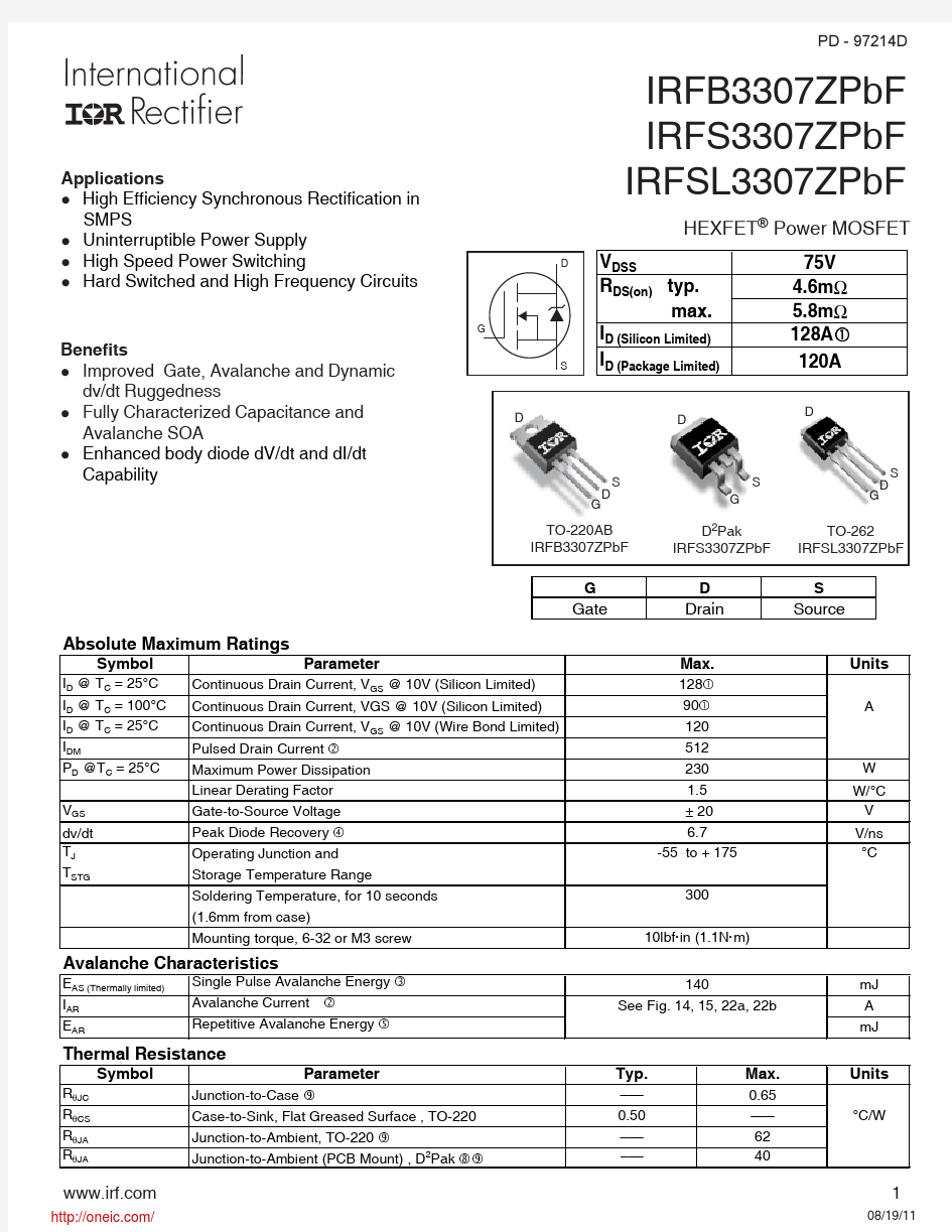

Benefits
l Improved Gate, Avalanche and Dynamic dv/dt Ruggedness
l Fully Characterized Capacitance and Avalanche SOA
l Enhanced body diode dV/dt and dI/dt Capability
IRFB3307ZPbF IRFS3307ZPbF IRFSL3307ZPbF
Applications
l High Efficiency Synchronous Rectification in SMPS
l Uninterruptible Power Supply l High Speed Power Switching
l Hard Switched and High Frequency Circuits
HEXFET ? Power MOSFET
D
S
G
D
S
D
G
TO-220AB IRFB3307ZPbF D 2Pak
IRFS3307ZPbF
TO-262
IRFSL3307ZPbF
S
D
G
D
PD - 97214D
IRFB/S/SL3307ZPbF
Notes:
Calculated continuous current based on maximum allowable junction temperature. Bond wire current limit is 120A. Note that current limitations arising from heating of the device leads may occur with some lead mounting arrangements.
Repetitive rating; pulse width limited by max. junction temperature.
Limited by T Jmax , starting T J = 25°C, L = 0.050mH
R G = 25Ω, I AS = 75A, V GS =10V. Part not recommended for use above this value.
I SD ≤ 75A, di/dt ≤ 1570A/μs, V DD ≤ V (BR)DSS , T J ≤ 175°C. Pulse width ≤ 400μs; duty cycle ≤ 2%.
C oss eff. (TR) is a fixed capacitance that gives the same charging time
as C oss while V DS is rising from 0 to 80% V DSS .
C oss eff. (ER) is a fixed capacitance that gives the same energy as C oss while V DS is rising from 0 to 80% V DSS .
When mounted on 1" square PCB (FR-4 or G-10 Material). For recom
mended footprint and soldering techniques refer to application note #AN-994. R θ is measured at T J approximately 90°C.
Static @ T = 25°C (unless otherwise specified)
IRFB/S/SL3307ZPbF Fig 1. Typical Output Characteristics
Fig 4. Normalized On-Resistance vs. Temperature
Fig 2. Typical Output Characteristics
Fig 6. Typical Gate Charge vs. Gate-to-Source Voltage Fig 5. Typical Capacitance vs. Drain-to-Source Voltage
V DS, Drain-to-Source Voltage (V)
110100
V DS, Drain-to-Source Voltage (V)
100
1000
10000
100000
C
,
C
a
p
a
c
i
t
a
n
c
e
(
p
F
)
T J , Junction Temperature (°C)
R
D
S
(
o
n
)
,
D
r
a
i
n
-
t
o
-
S
o
u
r
c
e
O
n
R
e
s
i
s
t
a
n
c
e
0102030405060708090
Q G,Total Gate Charge (nC)
0.0
2.0
4.0
6.0
8.0
10.0
12.0
V
G
S
,
G
a
t
e
-
t
o
-
S
o
u
r
c
e
V
o
l
t
a
g
e
(
V
)
IRFB/S/SL3307ZPbF
Fig 10. Drain-to-Source Breakdown Voltage
Fig 11. Typical C Stored Energy
Fig 9. Maximum Drain Current vs. Case Temperature
Fig 12. Maximum Avalanche Energy vs. DrainCurrent
0.1
1
10
100
1000
I S D , R e v e r s e D r a i n C u r r e n t (A )
T J , Temperature ( °C )
V (B R )D S S , D r a i n -t o -S o u r c e
B r e a k d o w n V o l t a g e (V )
20
30
40
50
60
70
80
V DS, Drain-to-Source Voltage (V)
0.0
0.20.40.60.8
1.01.2E n e r g y (μJ )
255075100125150175
Starting T J , Junction Temperature (°C)
100200300400500600E A S , S i n g l e P u l s e A v a l a n c h e E n e r g y (m J )
25
50
75
100
125
150
175
T C , Case Temperature (°C)020406080100120140I D , D r a i n C u r r e n t (A )
IRFB/S/SL3307ZPbF Fig 13. Maximum Effective Transient Thermal Impedance, Junction-to-Case
Fig 14. Typical Avalanche Current vs.Pulsewidth
Fig 15. Maximum Avalanche Energy vs. Temperature
Notes on Repetitive Avalanche Curves , Figures 14, 15:
(For further info, see AN-1005 at https://www.360docs.net/doc/069168974.html,)
1.Avalanche failures assumption:
Purely a thermal phenomenon and failure occurs at a temperature far in
excess of T jmax. This is validated for every part type.
2. Safe operation in Avalanche is allowed as long asT jmax is not exceeded.
3. Equation below based on circuit and waveforms shown in Figures 16a, 16b.
4. P D (ave) = Average power dissipation per single avalanche pulse.
5. BV = Rated breakdown voltage (1.3 factor accounts for voltage increase
during avalanche).
6. I av = Allowable avalanche current.
7. ΔT = Allowable rise in junction temperature, not to exceed T jmax (assumed as
25°C in Figure 14, 15).
t av = Average time in avalanche.
D = Duty cycle in avalanche = t av ·f
Z thJC(D, t av) = Transient thermal resistance, see Figures 13)
P D (ave) = 1/2 ( 1.3·BV·I av) =D T/ Z thJC
I av =2D T/ [1.3·BV·Z th]
E AS (AR) = P D (ave)·t av
t1 , Rectangular Pulse Duration (sec)
tav (sec)
A
v
a
l
a
n
c
h
e
C
u
r
r
e
n
t
(
A
)
Starting T J , Junction Temperature (°C)
E
A
R
,
A
v
a
l
a
n
c
h
e
E
n
e
r
g
y
(
m
J
)
IRFB/S/SL3307ZPbF
Fig. 17 - Typical Recovery Current vs. di f /dt
Fig 16. Threshold Voltage vs. Temperature
Fig. 19 - Typical Stored Charge vs. di f /dt
Fig. 18 - Typical Recovery Current vs. di f /dt
T J , Temperature ( °C )
V G S (t h ), G a t e t h r e s h o l d V o l t a g e (V )
200
400
600
800
1000
di F /dt (A/μs)
05
10
15
20
I R R (A
)
200
400
600
800
1000
di F /dt (A/μs)
20
100
180
260
340
420
Q R R (A
)
200
400
600
800
1000
di F /dt (A/μs)
05
10
15
20
I R R (A
)
200
400
600
800
1000
di F /dt (A/μs)
20
100
180
260
340
420
Q R R (A )
IRFB/S/SL3307ZPbF
Fig 22a. Switching Time Test Circuit Fig 22b.
Switching Time Waveforms
V V DS
90%
d(on)
d(off)
r
f
Fig 21b. Unclamped Inductive Waveforms
Fig 21a. Unclamped Inductive Test Circuit
I AS
V DD
Id
Qgs1Qgs2Qgd Qgodr
Fig 20. Peak Diode Recovery dv/dt Test Circuit for N-Channel
? Power MOSFETs
* V GS = 5V for Logic Level Devices
IRFB/S/SL3307ZPbF
TO-220AB Package Outline (Dimensions are shown in millimeters (inches))
D2Pak (TO-263AB) Package Outline Dimensions are shown in millimeters (inches)
分销商库存信息:
IR
IRFS3307ZTRLPBF IRFS3307ZPBF IRFB3307ZPBF IRFSL3307ZPBF