STB75NF75中文资料
1/11
June 2003
NEW DATASHEET ACCORDING TO PCN DSG20023123 MARKING: P75NF75 @
STB75NF75
STP75NF75 STP75NF75FP
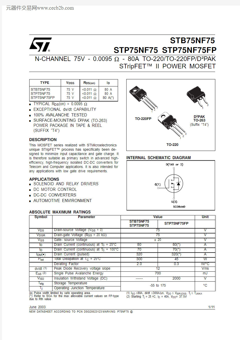
N-CHANNEL 75V - 0.0095 ? - 80A TO-220/TO-220FP/D2PAK
STripFET? II POWER MOSFET
s TYPICAL R DS (on) = 0.0095 ?
s EXCEPTIONAL dv/dt CAPABILITY s 100% AVALANCHE TESTED
s
SURFACE-MOUNTING D 2PAK (TO-263) POWER PACKAGE IN TAPE & REEL (SUFFIX “T4”)
DESCRIPTION
This MOSFET series realized with STMicroelectronics unique STripFET? process has specifically been de-signed to minimize input capacitance and gate charge. It is therefore suitable as primary switch in advanced high-efficiency, high-frequency isolated DC-DC converters for Telecom and Computer applications. It is also intended for any applications with low gate drive requirements.
APPLICATIONS
s SOLENOID AND RELAY DRIVERS s DC MOTOR CONTROL s DC-DC CONVERTERS
s AUTOMOTIVE ENVIRONMENT TYPE V DSS R DS(on)I D STB75NF75STP75NF75STP75NF75FP
75 V 75 V 75 V
<0.011 ?<0.011 ?<0.011 ?
80 A 80 A 80 A(*)
ABSOLUTE MAXIMUM RATINGS
Pulse width limited by safe operating area.
(*) Refer to SOA for the max allowable current values on FP-type due to Rth value
(1) I SD ≤80A, di/dt ≤300A/μs, V DD ≤ V (BR)DSS , T j ≤ T JMAX (2) Starting T j = 25 o C, I D = 40A, V DD = 37.5V
Symbol
Parameter
Value
Unit
STB75NF75 STP75NF75
STP75NF75FP V DS Drain-source Voltage (V GS = 0)75V V DGR Drain-gate Voltage (R GS = 20 k ?)75V V GS Gate- source Voltage
± 20
V I D Drain Current (continuous) at T C = 25°C 8080(*)A I D Drain Current (continuous) at T C = 100°C 7070(*)A I DM (?)Drain Current (pulsed)
320320(*)A P tot Total Dissipation at T C = 25°C 30045W Derating Factor
2.0
0.3
W/°C dv/dt (1)Peak Diode Recovery voltage slope 12V/ns E AS (2)Single Pulse Avalanche Energy 700
mJ V ISO Insulation Withstand Voltage (DC)------2000V T stg Storage Temperature
-55 to 175
°C
T j
Operating Junction Temperature
STB75NF75 STP75NF75 STP75NF75FP
2/11
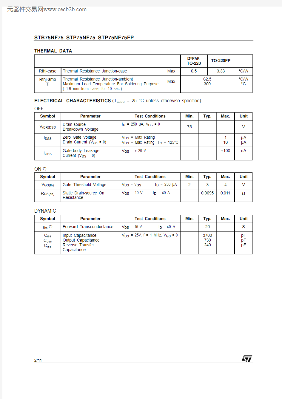
THERMAL DATA
ELECTRICAL CHARACTERISTICS (T case = 25 °C unless otherwise specified)OFF
ON (*)
DYNAMIC
D 2PAK TO-220
TO-220FP Rthj-case Thermal Resistance Junction-case
Max 0.5
3.33
°C/W Rthj-amb
T l
Thermal Resistance Junction-ambient
Maximum Lead Temperature For Soldering Purpose ( 1.6 mm from case, for 10 sec.)
Max
62.5300
°C/W °C
Symbol Parameter
Test Conditions
Min.Typ.
Max.
Unit V (BR)DSS Drain-source
Breakdown Voltage I D = 250 μA, V GS = 0
75
V I DSS
Zero Gate Voltage
Drain Current (V GS = 0)V DS = Max Rating
V DS = Max Rating T C = 125°C 110μA μA I GSS
Gate-body Leakage Current (V DS = 0)
V GS = ± 20 V
±100
nA
Symbol Parameter
Test Conditions
Min.Typ.Max.Unit V GS(th)Gate Threshold Voltage V DS = V GS I D = 250 μA 2
34V R DS(on)
Static Drain-source On Resistance
V GS = 10 V
I D = 40 A
0.0095
0.011
?
Symbol Parameter
Test Conditions
Min.
Typ.Max.
Unit g fs (*)Forward Transconductance V DS = 15 V
I D =40 A
20S C iss C oss C rss
Input Capacitance Output Capacitance Reverse Transfer Capacitance
V DS = 25V, f = 1 MHz, V GS = 0
3700730240
pF pF pF
3/11
STB75NF75 STP75NF75 STP75NF75FP
SWITCHING ON
SWITCHING OFF
SOURCE DRAIN DIODE
Pulsed: Pulse duration = 300 μs, duty cycle 1.5 %.(?)Pulse width limited by safe operating area.
Symbol Parameter
Test Conditions
Min.
Typ.Max.
Unit t d(on)t r Turn-on Delay Time Rise Time
V DD = 37.5 V
I D = 45 A R G =4.7 ? V GS = 10 V (Resistive Load, Figure 3)2525ns ns Q
g Q gs Q gd
Total Gate Charge Gate-Source Charge Gate-Drain Charge
V DD = 60 V I D = 80 A V GS = 10V
1172747
160nC nC nC
Symbol Parameter
Test Conditions
Min.
Typ.Max.
Unit t d(off)t f
Turn-off Delay Time Fall Time
V DD = 37.5 V
I D
= 45 A R G =4.7 ? V GS = 10 V (Resistive Load, Figure 3)
6630
ns ns
Symbol Parameter
Test Conditions
Min.
Typ.
Max.Unit I SD I SDM (?)Source-drain Current
Source-drain Current (pulsed)80320A A V SD (*)Forward On Voltage I SD = 80 A
V GS = 0
1.5
V t rr Q rr I RRM
Reverse Recovery Time Reverse Recovery Charge Reverse Recovery Current
I SD = 80 A
di/dt = 100A/μs V DD = 25 V T j = 150°C (see test circuit, Figure 5)
13266010
ns nC A
ELECTRICAL CHARACTERISTICS (continued)
STB75NF75 STP75NF75 STP75NF75FP
STB75NF75 STP75NF75 STP75NF75FP
STB75NF75 STP75NF75 STP75NF75FP
6/11
Fig. 3: Switching Times Test Circuits For Resistive
Fig. 5: Test Circuit For Inductive Load Switching
7/11
STB75NF75 STP75NF75 STP75NF75FP
DIM.mm.
inch.
MIN.TYP. MAX.
MIN.TYP. TYP .
A 4.4 4.60.1730.181A1 2.49 2.690.0980.106
A20.030.230.0010.009B 0.70.930.0280.037B2 1.14 1.70.0450.067C 0.450.60.0180.024C2 1.21 1.360.0480.054D 8.95
9.35
0.352
0.368
D18
0.315
E 1010.4
0.394
0.409
E18.50.334
G 4.88 5.280.1920.208L 1515.850.5910.624L2 1.27 1.40.0500.055L3 1.4 1.750.0550.069M 2.4
3.2
0.094
0.126
R 0.4
0.016
V2
0°8°
0°
8°
D 2PAK MECHANICAL DATA
STB75NF75 STP75NF75 STP75NF75FP
8/11
DIM.mm.
inch.
MIN.TYP. MAX.
MIN.TYP. TYP .
A 4.4 4.60.1730.181C 1.23 1.320.0480.051D 2.40 2.720.0940.107E 0.490.700.0190.027F 0.610.880.0240.034F1 1.14 1.700.0440.067F2 1.14 1.700.0440.067G 4.95 5.150.1940.203G1 2.40 2.700.0940.106H210
10.40
0.393
0.409
L216.400.645L328.90
1.137
L413140.5110.551L5 2.65 2.950.1040.116L615.2515.750.6000.620L7 6.20 6.600.2440.260L9 3.50 3.930.1370.154DIA
3.75
3.85
0.147
0.151
TO-220 MECHANICAL DATA
STB75NF75 STP75NF75 STP75NF75FP
10/11
DIM.
mm inch
MIN.MAX.MIN.MAX.
A010.510.70.4130.421
B015.715.90.6180.626
D 1.5 1.60.0590.063
D1 1.59 1.610.0620.063
E 1.65 1.850.0650.073
F11.411.60.4490.456
K0 4.8 5.00.1890.197
P0 3.9 4.10.1530.161
P111.912.10.4680.476
P2 1.9 2.100750.082
R50 1.574
T0.250.35.0.00980.0137
W23.724.30.9330.956
DIM.
mm inch
MIN.MAX.MIN.MAX.
A33012.992
B 1.50.059
C12.813.20.5040.520
D20.20.795
G24.426.40.960 1.039
N100 3.937
T30.4 1.197
BASE QTY BULK QTY
10001000
REEL MECHANICAL DATA
* on sales type
TUBE SHIPMENT (no suffix)* TAPE AND REEL SHIPMENT (suffix ”T4”)*
D2PAK FOOTPRINT
TAPE MECHANICAL DATA
STB75NF75 STP75NF75 STP75NF75FP Information furnished is believed to be accurate and reliable. However, STMicroelectronics assumes no responsibility for the consequences of use of such information nor for any infringement of patents or other rights of third parties which may result from its use. No license is granted
by implication or otherwise under any patent or patent rights of STMicroelectronics. Specifications mentioned in this publication are subject to change without notice. This publication supersedes and replaces all information previously supplied. STMicroelectronics products are not
authorized for use as critical components in life support devices or systems without express written approval of STMicroelectronics.
The ST logo is registered trademark of STMicroelectronics
? 2002 STMicroelectronics - All Rights Reserved
All other names are the property of their respective owners.
STMicroelectronics GROUP OF COMPANIES
Australia - Brazil - Canada - China - Finland - France - Germany - Hong Kong - India - Israel - Italy - Japan - Malaysia - Malta - Morocco - Singapore - Spain - Sweden - Switzerland - United Kingdom - United States.
https://www.360docs.net/doc/1f7273355.html,
11/11