GSCLM358中文资料
G S C L M 358 D U A L O P E R A T I O N A L A M P L I F I E R
Description The GSCLM358 consists of two independent high gain, internally frequency compensated operational amplifier. It can be operated from a Single power supply and also split power supplies. Features
*Internally frequency compensated for unity gain. *Wide power supply range 3V – 32V.
*Input common – mode voltage range include ground. *Large DC voltage gain.
Applications
*General purpose amplifier. *Transducer amplifier.
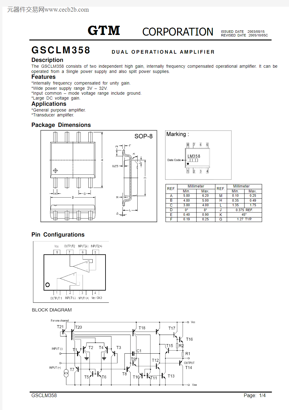
Package Dimensions
Millimeter Millimeter REF . Min. Max.
REF . Min. Max.
A 5.80 6.20 M 0.10 0.25
B 4.80 5.00 H 0.35 0.49
C 3.80 4.00 L 1.35 1.75
D 0° 8° J 0.375 REF.
E 0.40 0.90 K 45° F
0.19
0.25
G
1.27 TYP .
Pin Configurations
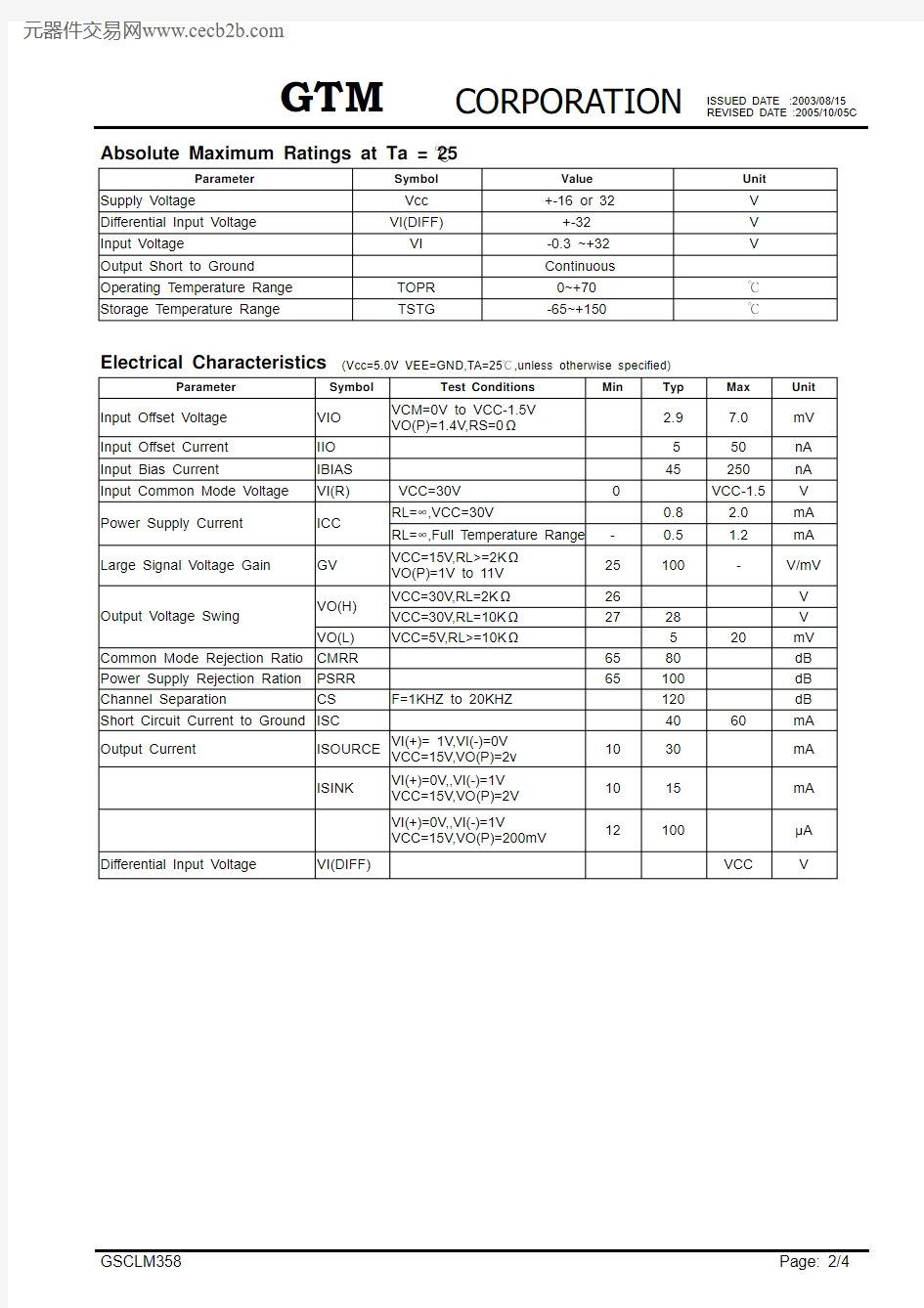
Absolute Maximum Ratings at Ta = 25
Parameter Symbol Value Unit Supply Voltage Vcc +-16 or 32V Differential Input Voltage VI(DIFF) +-32 V
Input Voltage VI-0.3 ~+32V
Output Short to Ground Continuous
Operating Temperature Range TOPR 0~+70 Storage Temperature Range TSTG -65~+150
Electrical Characteristics (Vcc=5.0V VEE=GND,TA=25 ,unless otherwise specified)
Parameter Symbol Test Conditions Min Typ Max Unit Input Offset Voltage VIO VCM=0V to VCC-1.5V
VO(P)=1.4V,RS=0 2.9 7.0 mV Input Offset Current IIO 5 50 nA Input Bias Current IBIAS 45 250 nA Input Common Mode Voltage VI(R) VCC=30V 0 VCC-1.5 V
RL= ,VCC=30V 0.8 2.0 mA Power Supply Current ICC
RL= ,Full Temperature Range - 0.5 1.2 mA
Large Signal Voltage Gain GV VCC=15V,RL>=2K
VO(P)=1V to 11V 25 100 - V/mV
VCC=30V,RL=2K 26 V
VO(H)
Output Voltage Swing
VCC=30V,RL=10K 27 28 V
VO(L) VCC=5V,RL>=10K 5 20 mV Common Mode Rejection Ratio CMRR 65 80 dB Power Supply Rejection Ration PSRR 65 100 dB Channel Separation CS F=1KHZ to 20KHZ 120 dB Short Circuit Current to Ground ISC 40 60 mA
Output Current ISOURCE VI(+)= 1V,VI(-)=0V
VCC=15V,VO(P)=2v 10 30 mA
ISINK VI(+)=0V,,VI(-)=1V
VCC=15V,VO(P)=2V 10 15 mA
VI(+)=0V,,VI(-)=1V
VCC=15V,VO(P)=200mV 12 100 A Differential Input Voltage VI(DIFF) VCC V
Characteristics Curve
Important Notice:
All rights are reserved. Reproduction in whole or in part is prohibited without the prior written approval of GTM.
GTM reserves the right to make changes to its products without notice.
GTM semiconductor products are not warranted to be suitable for use in life-support Applications, or systems.
GTM assumes no liability for any consequence of customer product design, infringement of patents, or application assistance. Head Office And Factory:
Taiwan: No. 17-1 T atung Rd. Fu Kou Hsin-Chu Industrial Park, Hsin-Chu, T aiwan, R. O. C.
TEL : 886-3-597-7061 FAX : 886-3-597-9220, 597-0785
China: (201203) No.255, Jang-Jiang T sai-Lueng RD. , Pu-Dung-Hsin District, Shang-Hai City, China
TEL : 86-21-5895-7671 ~ 4 FAX : 86-21-38950165