GT15Q301_06中文资料
TOSHIBA INSULATED GATE BIPOLAR TRANSISTOR SILICON N CHANNEL IGBT
GT15Q301
HIGH POWER SWITCHING APPLICATIONS MOTOR CONTROL APPLICATIONS
z Third-generation IGBT z Enhancement mode type z High speed
: t f = 0.32 μs (Max.) z Low saturation voltage : V CE (sat) = 2.7 V (Max.)
z FRD included between emitter and collector
ABSOLUTE MAXIMUM RATINGS (Ta = 25°C)
CHARACTERISTIC SYMBOL RATING
UNIT
Collector ?Emitter Voltage V CES 1200 V Gate ?Emitter Voltage V GES
±20 V
DC I C 15 A Collector Current
1ms I CP 30
A DC I F 15 A Emitter ?Collector Forward
Current
1ms I FM 30
A Collector Power Dissipation (Tc = 25°C)
P C 170
W Junction Temperature Tj 150 °C Storage Temperature Range
T stg
?55~150
°C
Note: Using continuously under heavy loads (e.g. the application of high temperature/current/voltage and the
significant change in temperature, etc.) may cause this product to decrease in the reliability significantly even if the operating conditions (i.e. operating temperature/current/voltage, etc.) are within the absolute maximum ratings.
Please design the appropriate reliability upon reviewing the Toshiba Semiconductor Reliability Handbook
(“Handling Precautions”/Derating Concept and Methods) and individual reliability data (i.e. reliability test report and estimated failure rate, etc).
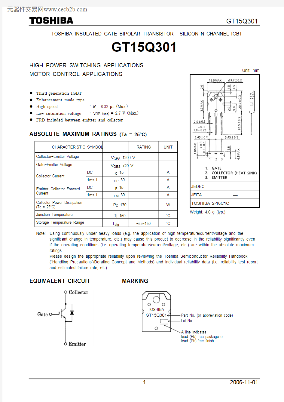
EQUIVALENT CIRCUIT MARKING
Unit: mm
JEDEC ? JEITA ?
TOSHIBA 2-16C1C Weight: 4.6 g (typ.)
lead (Pb)-free package or lead (Pb)-free finish.
ELECTRICAL CHARACTERISTICS (Ta = 25°C)
CHARACTERISTIC SYMBOL TEST CONDITION MIN TYP. MAX
UNIT
Gate Leakage Current I GES V GE = ±20 V, V CE = 0 ― ― ±500
nA
Collector Cut ?Off Current I CES V CE = 1200 V, V GE = 0 ― ― 1.0 mA Gate-Emitter Cut ?Off Voltage V GE (OFF) I C = 1.5 mA, V CE = 5 V 4.0
― 7.0 V
Collector ?Emitter Saturation Voltage V CE (sat) I C = 15 A, V GE = 15 V
― 2.1 2.7 V Input Capacitance
C ies V CE = 50 V, V GE = 0, f = 1 MHz ― 950 ― pF Rise Time
t r ― 0.05 ― Turn ?On Time t on ― 0.12 ― Fall Time t f ― 0.16 0.40Switching Time
Turn ?Off Time
t off Inductive Load
V CC = 600 V, I C = 15 A V GG = ±15 V, R G = 56 ?
(Note)
― 0.56 ― μs
Peak Forward Voltage V F I F = 15 A, V GE = 0
― ― 3.0 V Reverse Recovery Time t rr I F = 15 A, di / dt = ?200 A / μs
― ― 350ns Thermal Resistance (IGBT) R th (j ?c) ― ― ― 0.74°C / W Thermal Resistance (Diode)
R th (j ?c)
―
―
―
1.56
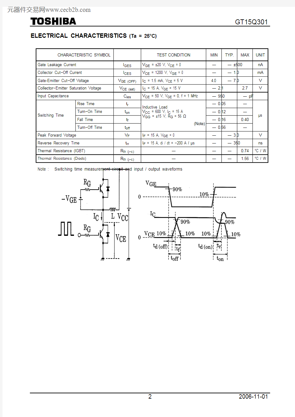
°C / W Note : Switching time measurement circuit and input / output waveforms
RESTRICTIONS ON PRODUCT USE
20070701-EN ?The information contained herein is subject to change without notice.
?TOSHIBA is continually working to improve the quality and reliability of its products. Nevertheless, semiconductor devices in general can malfunction or fail due to their inherent electrical sensitivity and vulnerability to physical stress. It is the responsibility of the buyer, when utilizing TOSHIBA products, to comply with the standards of safety in making a safe design for the entire system, and to avoid situations in which a malfunction or failure of such TOSHIBA products could cause loss of human life, bodily injury or damage to property.
In developing your designs, please ensure that TOSHIBA products are used within specified operating ranges as set forth in the most recent TOSHIBA products specifications. Also, please keep in mind the precautions and conditions set forth in the “Handling Guide for Semiconductor Devices,” or “TOSHIBA Semiconductor Reliability Handbook” etc.
? The TOSHIBA products listed in this document are intended for usage in general electronics applications (computer, personal equipment, office equipment, measuring equipment, industrial robotics, domestic appliances, etc.).These TOSHIBA products are neither intended nor warranted for usage in equipment that requires extraordinarily high quality and/or reliability or a malfunction or failure of which may cause loss of human life or bodily injury (“Unintended Usage”). Unintended Usage include atomic energy control instruments, airplane or spaceship instruments, transportation instruments, traffic signal instruments, combustion control instruments, medical instruments, all types of safety devices, etc.. Unintended Usage of TOSHIBA products listed in his document shall be made at the customer’s own risk.
?The products described in this document shall not be used or embedded to any downstream products of which manufacture, use and/or sale are prohibited under any applicable laws and regulations.
? The information contained herein is presented only as a guide for the applications of our products. No responsibility is assumed by TOSHIBA for any infringements of patents or other rights of the third parties which may result from its use. No license is granted by implication or otherwise under any patents or other rights of TOSHIBA or the third parties.
? Please contact your sales representative for product-by-product details in this document regarding RoHS compatibility. Please use these products in this document in compliance with all applicable laws and regulations that regulate the inclusion or use of controlled substances. Toshiba assumes no liability for damage or losses occurring as a result of noncompliance with applicable laws and regulations.