IRF7493TRPBF;IRF7493PBF;中文规格书,Datasheet资料

https://www.360docs.net/doc/1511023211.html, 1
09/21/04
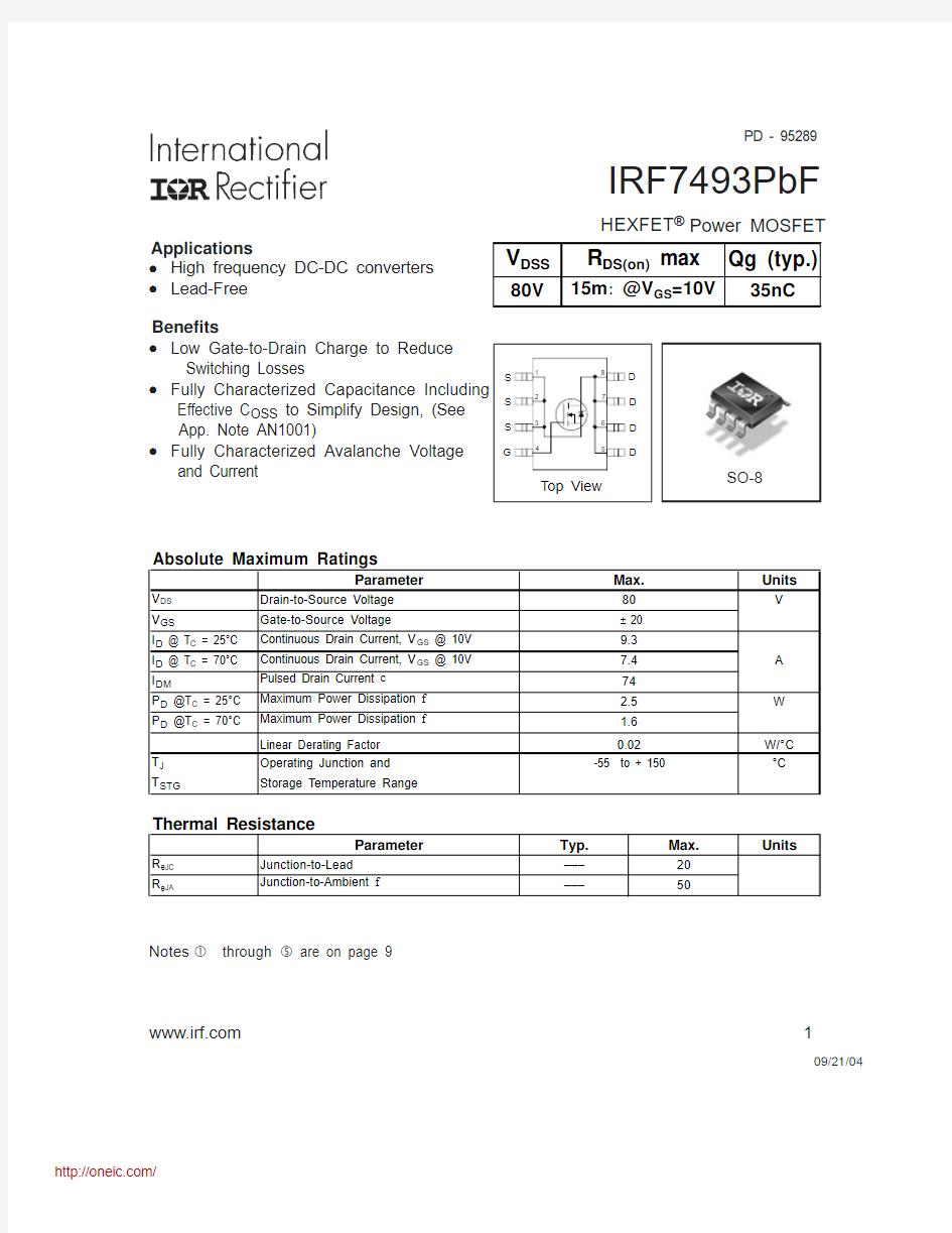
SO-8
IRF7493PbF
HEXFET ? Power MOSFET
Notes through are on page 9
PD - 95289
l High frequency DC-DC converters l Lead-Free
Benefits
Applications
l Low Gate-to-Drain Charge to Reduce Switching Losses
l Effective C OSS to Simplify Design, (See App. Note AN1001)
l Fully Characterized Avalanche Voltage and Current
IRF7493PbF
https://www.360docs.net/doc/1511023211.html,
DD = 15V GS = 0V e
IRF7493PbF
https://www.360docs.net/doc/1511023211.html, 3
Fig 2. Typical Output Characteristics
Fig 1. Typical Output Characteristics Fig 3. Typical Transfer Characteristics
Fig 4. Normalized On-Resistance
Vs. Temperature
V DS , Drain-to-Source Voltage (V)
V DS , Drain-to-Source Voltage (V)
V GS , Gate-to-Source Voltage (V)
-60-40-20
20
40
60
80100120140160
T J , Junction Temperature (°C)
0.5
1.0
1.5
2.0
R D S (o n ) , D r a i n -t o -S o u r c e O n R e s i s t a n c e (N o r m a l i z e d )
IRF7493PbF
https://www.360docs.net/doc/1511023211.html,
Fig 6. Typical Gate Charge Vs.
Gate-to-Source Voltage
Fig 5. Typical Capacitance Vs.
Drain-to-Source Voltage
Fig 7. Typical Source-Drain Diode
Forward Voltage
Fig 8. Maximum Safe Operating Area
1
10
100
V DS , Drain-to-Source Voltage (V)
10
100
1000
10000
100000
C , C a p a c i t a n c e (p F )
10
20
30
40
50
60
Q G Total Gate Charge (nC)
04
8
12
16
20
V
G S , G a t e -t o -S o u r c e V o l t a g e (V )
0.2
0.4
0.6
0.8
1.0
1.2
V SD , Source-toDrain Voltage (V)
0.1
1.0
10.0
100.0I S D , R e v e r s e D r a i n C u r r e n t (A )
1
10
1001000
V DS , Drain-toSource Voltage (V)
0.1
1
10
100
1000
I D , D r a i n -t o -S o u r c e C u r r e n t (A
)
IRF7493PbF
https://www.360docs.net/doc/1511023211.html, 5
Fig 11. Maximum Effective Transient Thermal Impedance, Junction-to-Ambient
Fig 10a.
Switching Time Test Circuit
V V d(on)
r
d(off)
f
Fig 10b. Switching Time Waveforms
V DD
Fig 9. Maximum Drain Current Vs.
Ambient Temperature
25
50
75
100
125
150
T C , Case Temperature (°C)
02
4
6
810
I D , D r a i n C u r r e n t (A )
IRF7493PbF
https://www.360docs.net/doc/1511023211.html,
Fig 13. On-Resistance Vs. Gate Voltage
Fig 12. On-Resistance Vs. Drain Current
Fig 14a&b. Basic Gate Charge Test Circuit
and Waveform
Fig 15a&b. Unclamped Inductive Test circuit
and Waveforms
Fig 15c. Maximum Avalanche Energy
Vs. Drain Current
DS
Current Sampling Resistors
V
GS
V
I
V DD
V GS, Gate -to -Source Voltage (V)
, D r a i n -t o -S o u r c e O n R e s i s t a n c e (?)
255075100125150
Starting T J , Junction Temperature (°C)
100
200
300
400
500
E A S , S i n g l e P u l s e A v a l a n c h e E n e r g y (m J )
20
40
60
80
I D , Drain Current (A)
0.011
0.012
0.013
R D S (o n ) , D r a i n -t o -S o u r c e O n R e s i s t a n c e (?)
IRF7493PbF
https://www.360docs.net/doc/1511023211.html, 7
Fig 16. Peak Diode Recovery dv/dt Test Circuit for N-Channel
HEXFET ? Power MOSFETs
* V GS = 5V for Logic Level Devices
Fig 17. Gate Charge Waveform
Id
Qgs1Qgs2Qgd Qgodr
IRF7493PbF
SO-8 Package Outline
IRF7493PbF
https://www.360docs.net/doc/1511023211.html, 9
Repetitive rating; pulse width limited by
max. junction temperature.
Notes:
Starting T J = 25°C, L = 12mH
R G = 25?, I AS = 5.6A.
Pulse width ≤ 300μs; duty cycle ≤ 2%.
When mounted on 1 inch square copper board
C oss eff. is a fixed capacitance that gives the same charging time
as C oss while V DS is rising from 0 to 80% V DSS
330.00(12.992) MAX.
14.40 ( .566 )12.40 ( .488 )
NOTES :
1. CONTROLLING DIMENSION : MILLIMETER.
2. OUTLINE CONFORMS TO EIA-481 & EIA-541.
FEED DIRECTION
TERMINAL NUMBER 1
12.3 ( .484 )11.7 ( .461 )
8.1 ( .318 )7.9 ( .312 )
NOTES:
1. CONTROLLING DIMENSION : MILLIMETER.
2. ALL DIMENSIONS ARE SHOWN IN MILLIMETERS(INCHES).
3. OUTLINE CONFORMS TO EIA-481 & EIA-541.
SO-8 Tape and Reel
Dimensions are shown in millimeters (inches)
Data and specifications subject to change without notice.
This product has been designed and qualified for the Consumer market.
Qualifications Standards can be found on IR’s Web site.
IR WORLD HEADQUARTERS: 233 Kansas St., El Segundo, California 90245, USA Tel: (310) 252-7105
TAC Fax: (310) 252-7903
Visit us at https://www.360docs.net/doc/1511023211.html, for sales contact information .09/04
分销商库存信息:
IR
IRF7493TRPBF IRF7493PBF