HLMP-HB61中文资料

HLMP-HD61, HLMP-HM61 and HLMP-HB61
Precision Optical Performance Red, Green and Blue 5mm Standard Oval LEDs
Data Sheet
Description
These Precision Optical Performance Oval LEDs are specifically designed for full color/video and passenger information signs. The oval shaped radiation pattern and high luminous intensity ensure that these devices are excellent for wide field of view outdoor applications where a wide viewing angle and readability in sunlight are essential. These lamps have very smooth, matched radiation patterns ensuring consistent color mixing in full color applications, message uniformity across the viewing angle of the sign. High efficiency LED material is used in these lamps: Aluminum Indium Gallium Phos-phide (AlInGaP II) for red and Indium Gallium Nitride for blue and green. Each lamp is made with an advanced optical grade epoxy offering superior high temperature and high moisture resistance in outdoor applications.
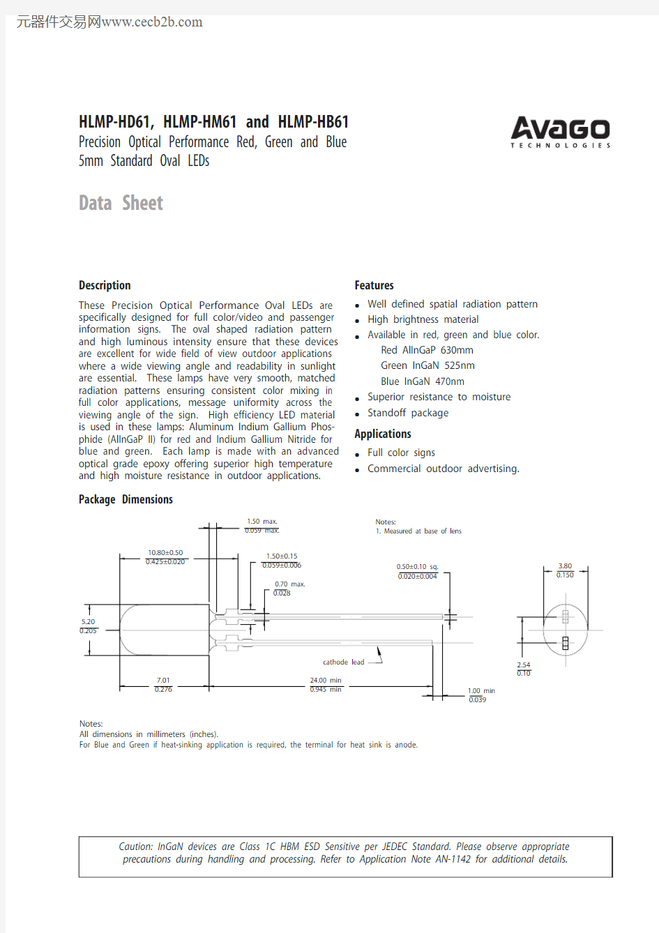
Package Dimensions
Notes:
All dimensions in millimeters (inches).
For Blue and Green if heat-sinking application is required, the terminal for heat sink is anode.
Features
? Well defined spatial radiation pattern ? High brightness material
? Available in red, green and blue color. Red AlInGaP 630mm Green InGaN 525nm Blue InGaN 470nm
? Superior resistance to moisture ? Standoff package
Applications
? Full color signs
?
Commercial outdoor advertising.
Device Selection Guide
Part Numbering System
Tolerance for each intensity limit is ± 15%.
Notes:
1. The luminous intensity is measured on the mechanical axis of the lamp package.
Packaging Option ZZ: Flexi Ammo-packs Color Bin Selection 0: Open distribution
T: Red Color, Vf max =2.6V Maximum Intensity Bin
0: No maximum intensity limit Minimum Intensity Bin
Refer to Device Selection Guide.Color
B: Blue 470D: Red 630M: Green 525
Package
H: 5mm Standard Oval 40? x 100??
Part Number
Color and Dominant Wavelength l d (nm) Typ
Luminous Intensity l v (mcd) at 20 mA Min
Luminous Intensity l v (mcd) at 20 mA Max
HLMP-HD61-TXTZZ Red 6308001990HLMP-HM61-Y30ZZ Green 52519905040HLMP-HB61-QU0ZZ
Blue 470
460
1150
Notes:
1. For option –xxTxx, the VF maximum is
2.6V, refer to Vf bin table
2. The dominant wavelength is derived from the chromaticity Diagram and represents the color of the lamp
3. The radiant intensity, I e in watts per steradian, may be found from the equation I e = I V /ηV where I V is the luminous intensity in candelas and ηV is the luminous efficacy in lumens/watt.
4. Forward voltage allowable tolerance is ± 0.05V.
5. For AlInGaP Red, thermal resistance applied to LED junction to cathode lead. For InGaN blue and Green, thermal resistance applied to LED junction to anode lead.
Electrical / Optical Characteristics (T A = 25°C)
Notes:
1. Derate linearly as shown in Figure 2 and Figure 8.
2. Duty Factor 30%, frequency 1KHz.
3. Duty Factor 10%, frequency 1KHz.
Absolute Maximum Rating (T A = 25°C)
Parameter
Red
Blue and Green
Unit
DC Forward Current [1]5030mA Peak Forward Current 100[2]100[3]mA Power Dissipation 130
116mW Reverse Voltage
5 (I R = 100 m A) 5 (I R = 10 m A)V LED Junction Temperature 130110°C Operating Temperature Range -40 to +100-40 to +85°C Storage Temperature Range
-40 to +120
-40 to +100
°C
Parameter
Symbol
Min.
Typ.
Max.
Units
Test Conditions
Forward Voltage Red Green Blue V F
2.02.82.8 2.3
3.33.2
2.6[1]
3.83.8
V
I F = 20 mA
Reverse Voltage Red
Green & blue V R 55V
I R = 100 m A I R = 10 m A Dominant Wavelength Red Green Blue
l D
622520460
630525470634540480
nm
I F = 20 mA
Peak Wavelength Red Green Blue
l PEAK
639516464nm
Peak of Wavelength of Spectral Distribution at I F = 20 mA
Spectral Half width Red Green Blue
Dl 1/2
173223nm
Wavelength Width at Spectral Distribution ? Power Point at ,I F = 20 mA Thermal Resistance,R q J-PIN 240°C/W LED Junction-to-pin
Luminous Efficacy [3] Red Green Blue
ηV
15552075
lm/W
Emitted Luminous Power/Emitted Radiant Power
WAVELENGTH – nm
R E L A T I V E I N T E N S I T Y
1.00.5
600700
6505500
4020I F - F O R W A R D C U R R E N T - m A
V F - FORWARD VOLTAGE - V
103050R E L A T I V E I N T E N S I T Y (N O R M A L I Z E D A T 20 m A )
FORWARD CURRENT - mA
2.01.00.5
1.5
2.5AlInGaP Red
Figure 1. Relative Intensity vs Wavelength
Figure 2. Maximum Forward Current vs Ambient Temperature
Figure 3. Forward Current vs Forward Voltage Figure 4. Relative Intensity vsForward Current
102030405060T A - AMBIENT TEMPERATURE -o C
I F M A X .- M A X I M U M F O R W A R D C U R R E N T - m A
WAVELENGTH - nm
R E L A T I V E I N T E N S I T Y
0051015202530350
2
4
FORWARD VOLTAGE - V
F O R W A R D C U R R E N T - m A
1300.20.40.60.81.01.21.41.60
5
10
15
20
25
30
DC FORWARD CURRENT - mA
R E L A T I V E L U M I N O U S I N T E N S I T Y (N O R M A L
I Z E D A T 20 m A )
051015202530350
20
40
60
80
100
T A - AMBIENT TEMPERATURE - o C
I F - M A X I M U M F O R W A R D C U R R E N T - m A
InGaN Blue and Green
Figure 5. Relative Intensity vs Wavelength
Figure 6. Forward Current vs Forward Voltage
Figure 7. Relative Intensity vs Forward Current
Figure 8. Maximum Forward Current vs Ambient Temperature
Figure 9. Relative dominant wavelength vs Forward Current
Figure 10. Radiation pattern-Major Axis
Figure 11. Radiation pattern-Minor Axis
00.20.40.60.81-90
-60
-30
30
60
90
ANGULAR DISPLACEMENT - DEGREES
N O R M A L I Z E D I N T E N S I T
Y 00.20.40.60.81-90
-60-300306090
ANGULAR DISPLACEMENT - DEGREES
N O R M A L I Z E D I N T E N S I T Y -4-202468100
5
1015202530
FORWARD CURRENT - mA
BLUE
GREEN
R E L A T I V E D O M I N A N T W A V E L E N G H T S H I F T (N O R M A L I Z E D A T 20m A )
Intensity Bin Limit Table (1.2: 1 Iv Bin Ratio)
Blue Color Bin Table
Green Color Bin Table
VF bin Table (V at 20mA)
Red Color Range
Tolerance for each bin limit is ± 0.5nm
Note:
1. All bin categories are established for classification of products. Products may not be available in all bin categories. Please contact your Avago representative for further information.
Tolerance for each bin limit is ± 0.5nm
Tolerance for each bin limit is ± 0.5 nm
Tolerance for each bin limit is ± 0.05
Tolerance for each bin limit is ± 15%
Bin
Min Dom
Max Dom
Xmin
Ymin
Xmax
Ymax
1
460.0464.00.14400.02970.17660.09660.18180.09040.13740.03742464.0468.00.13740.03740.16990.10620.17660.09660.12910.04953468.0472.00.12910.04950.16160.12090.16990.10620.11870.06714472.0476.00.11870.06710.15170.14230.16160.12090.10630.09455
476.0
480.0
0.10630.09450.13970.17280.1517
0.1423
0.0913
0.1327
Bin
Min Dom
Max Dom
Xmin
Ymin
Xmax
Ymax
1520.0524.00.07430.83380.18560.65560.16500.65860.10600.82922524.0528.00.10600.82920.20680.64630.18560.65560.13870.81483528.0532.00.13870.81480.22730.63440.20680.64630.17020.79654532.0536.00.17020.79650.24690.62130.22730.63440.20030.77645
536.0
540.0
0.20030.77640.26590.60700.2469
0.6213
0.2296
0.7543
Min Dom
Max Dom
Xmin Ymin Xmax Ymax
622
634
0.69040.30940.69450.28880.67260.31060.7135
0.2865
Bin ID
Min.
Max.
VA 2.0 2.2VB 2.2 2.4VC
2.4
2.6
Bin
Intensity (mcd) at 20 mA
Min Max Q 460550R 550660S 660800T 800960U 9601150V 11501380W 13801660X 16601990Y 19902400Z 240029001290035002350042003
4200
5040
Avago Color Bin on CIE 1931 Chromaticity Diagram
Relative Light Output vs. Junction Temperature
-40
-20020406080100
T J - JUNCTION TEMPERATURE - ?C
R E L A T I V
E L I G H T O U T P U T (N O R M A L I Z E D a t T J = 25?C )
0.000
0.200
0.400
0.6000.800
1.000
0.000
0.100
0.200
0.300
0.4000.500
0.600
0.700
0.800
X
Y
? Wave soldering parameter must be set and maintain according to recommended temperature and dwell time in the solder wave. Customer is advised to daily check on the soldering profile to ensure the soldering profile used is always conforming to recommended soldering condition.
Note:
1. PCB with different size and design (component density) will have different heat mass (heat capacity). This might cause a change in temperature experienced by the board if same wave soldering setting is used. So, it is recommended to re-calibrate the solder-ing profile again prior to loading a new type of PCB.
2. Avago Technologies’ high brightness LED are using high effi-ciency LED die with single wire bond as shown below. Customer is advised to take extra precaution during wave soldering to ensure that the maximum wave temperature is not exceeding recommendation of 250 ° C. Over-stressing the LED during sol-dering process might cause premature failure to the LED due to delamination.
Precautions
Lead Forming:
? The leads of an LED lamp may be preformed or cut to length prior to insertion and soldering into PC board.
? If lead forming is required before soldering, care must be taken to avoid any excessive mechanical stress induced to LED package. Otherwise, cut the leads of LED to length after soldering process at room temperature. The solder joint formed will absorb the mechanical stress of the lead cutting from traveling to the LED chip die attach and wirebond.
? For better control, it is recommended to use proper tool to precisely form and cut the leads to length rather that doing it manually.Soldering Condition:
? Care must be taken during PCB assembly and solder-ing process to prevent damage to LED component.? The closest manual soldering distance of the solder-ing heat source (soldering iron’s tip) to the body is 1.59mm. Soldering the LED closer than 1.59mm might damage the LED.
LED component Lead size
Diagonal Plated through hole diameter 0.457 x 0.457mm (0.018 x 0.018inch)0.646 mm (0.025 inch)0.976 to 1.078 mm (0.038 to 0.042 inch)0.508 x 0.508mm (0.020 x 0.020inch)
0.718 mm (0.028 inch)
1.049 to 1.150mm (0.041 to 0.045 inch)
Wave Soldering
Manual Solder Dipping Pre-heat temperature 105 °C Max.-Preheat time 30 sec Max -Peak temperature 250 °C Max.260 °C Max.Dwell time
3 sec Max.
5 sec Max
Note: Refer to application note AN1027 for more information
on soldering LED components.
AlInGaP Device
InGaN Device
? Recommended soldering condition:
Avago Technologies LED configuration
Note: Electrical connection between bottom surface of LED die and the leadframe material through conductive paste or solder.
? If necessary, use fixture to hold the LED component in proper orientation with respect to the PCB during soldering process.
Note: In order to further assist customer in designing jig accurately that fit Avago Technologies’ product, 3D model of the product is available upon request.
? At elevated temperature, the LED is more susceptible to mechanical stress. Therefore, PCB must be allowed to cool down to room temperature prior to handling, which includes removal of jigs, fixtures or pallet.
? Special attention must be given to board fabrication, solder masking, surface plating and lead holes size and component orientation to assure solderability. ? Recommended PC board plated through holes size for LED component leads.
? Over sizing of plated through hole can lead to twisting or improper LED placement during auto insertion. Un-der sizing plated through hole can lead to mechanical stress on the epoxy lens during clinching
BOTTOM SIDE TOP SIDE NOTE: ALLOW FOR BOARDS TO BE CONVEYOR SPEED = 1.83 M/MIN (6 FT/MIN)250
200150
TIME - SECONDS
T E M P E R A T U R E - °C
100
5030
LEAD FREE SOLDER
96.5%Sn; 3.0%Ag; 0.5% Cu SUFFICIENTLY COOLED BEFORE EXERTING MECHANICAL FORCE.
OF PC BOARD
OF PC BOARD PREHEAT SETTING = 150°C (100°C PCB)
SOLDER WAVE TEMPERATURE = 245°C ± 5°C AIR KNIFE AIR TEMPERATURE = 390°C AIR KNIFE DISTANCE = 1.91 mm (0.25 IN.)SOLDER: SN63; FLUX: RMA AIR KNIFE ANGLE = 40
Ammo Packs Drawing
Note: The ammo-packs drawing is applicable for packaging option –DD & - ZZ and regardless standoff or non-standoff
Note: For InGaN device, the ammo pack packaging box contain ESD logo
For product information and a complete list of distributors, please go to our web site: https://www.360docs.net/doc/1d11952031.html,
Avago, Avago Technologies, and the A logo are trademarks of Avago Technologies, Limited in the United States and other countries. Data subject to change. Copyright ? 2006 Avago Technologies Limited. All rights reserved. Obsoletes AV01-0418EN AV02-0339EN - April 19, 2007
DISCLAIMER: AVAGO’S PRODUCTS AND SOFTWARE ARE NOT SPECIFICALLY DESIGNED, MANUFACTURED OR AUTHORIZED FOR SALE AS PARTS, COMPONENTS OR ASSEMBLIES FOR THE PLANNING, CONSTRUCTION, MAINTENANCE OR DIRECT OPERATION OF A NUCLEAR FACILITY OR FOR USE IN MEDICAL DEVICES OR APPLI-CATIONS. CUSTOMER IS SOLELY RESPONSIBLE, AND WAIVES ALL RIGHTS TO MAKE CLAIMS AGAINST AVAGO OR ITS SUPPLIERS, FOR ALL LOSS, DAMAGE, EXPENSE OR LIABILITY IN CONNECTION WITH SUCH USE.