AIC1578中文资料
High-Efficiency, Step-Down DC/DC Converter
Analog Integrations Corporation 4F, 9, Industry E. 9th Rd, Science Based Industrial Park, Hsinchu Taiwan, ROC https://www.360docs.net/doc/1c12713521.html,
FEATURES
?4V to 20V Input Voltage Operation.?High Efficiency (up to 95%).
?Low Quiescent Current at 90μA.
?Pulse-Skipping and Pulse-Frequency Modulation.?Inputs-Uncommitted Current Sense Comparator.?Duty Cycle Adjustable.
?90KHz to 280KHz Oscillator Frequency.?Power-Saving Shutdown Mode (8μA Typical).?Push-Pull Driver Output.
APPLICATIONS
?Notebook 5V/3.3V Main Power
?Step-Down DC/DC Converter Module.
? Constant Current Source for Battery Chargers.
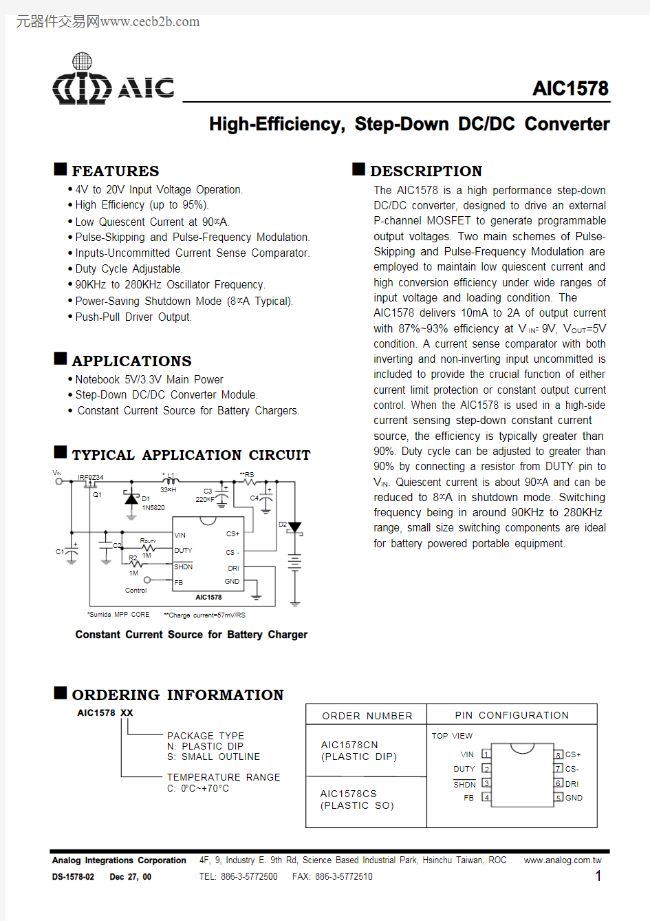
TYPICAL APPLICATION CIRCUIT
**Charge current=57mV/RS
*Sumida MPP CORE
Constant Current Source for Battery Charger
DESCRIPTION
The AIC1578 is a high performance step-down DC/DC converter, designed to drive an external P-channel MOSFET to generate programmable output voltages. Two main schemes of Pulse-Skipping and Pulse-Frequency Modulation are employed to maintain low quiescent current and high conversion efficiency under wide ranges of input voltage and loading condition. The AIC1578 delivers 10mA to 2A of output current with 87%~93% efficiency at V IN =9V, V OUT =5V condition. A current sense comparator with both inverting and non-inverting input uncommitted is included to provide the crucial function of either current limit protection or constant output current control. When the AIC1578 is used in a high-side current sensing step-down constant current source, the efficiency is typically greater than 90%. Duty cycle can be adjusted to greater than 90% by connecting a resistor from DUTY pin to V IN . Quiescent current is about 90μA and can be reduced to 8μA in shutdown mode. Switching frequency being in around 90KHz to 280KHz range, small size switching components are ideal for battery powered portable equipment.
ORDERING INFORMATION
ABSOLUTE MAXIMUM RATINGS
VIN Supply Voltage.....…………............................................................................. 20V
DUTY Voltage.........................................……………................................................ 20V
SHDN Voltage......................................………….................................................... 15V
Operating Temperature Range................…………......................................... 0°C~70°C
Storage Temperature Range......................…………................................. -65°C~ 150°C
TEST CIRCUIT
Refer to Fig. 1 circuit of Application Examples.
ELECTRICAL CHARACTERISTICS(V IN= 13V, Ta=25°C, unless otherwise
TYPICAL PERFORMANCE CHARACTERISTICS
V IN ( V)
D u t y (%)
F r
e q u e n c y (K H z )
Temperature (°C)
Duty Cycle vsTemperature
D u t y C y c l e (%)
Temperature (°C)Frequency vs Temperature
F r e q u e n c y (K H z )
90140
190
240
290
R DUTY (M ?)
Duty Cycle vs R DUTY
D u t y C y c l e (%)
1
234
V IN (V)
S h u t d o w n C u r r e n t (μA )
20
46810121416180
5
10
1520
V IN (V)
Quiescent Current vs V IN
Q u i e s c e n t C u r r e n t (μA )
11
BLOCK DIAGRAM
DUTY
FB
SHDN
VIN
PIN DESCRIPTIONS
PIN 1:VIN
-4V to 20V input supply voltage.
PIN 2:DUTY-Duty cycle adjustment pin. To be
tied to the VIN pin directly or through a resistor R DUTY to adjust oscillator duty cycle. R DUTY must be above 1M ? if V IN =20V.
See TYPICAL PERFORMANCE CHARACTERISTICS.PIN 3:SHDN -Logical input to shutdown the
chip:
V SHDN =
High for normal operation.
V SHDN = Low for shutdown.
This pin should not be floating or forced to greater than 15V. In shutdown mode DRI pins is at high level.PIN 4:FB
-Feedback comparator input, to
compare the feedback voltage with the internal reference
voltage. Connecting a resistor R1to converter output node and a resistor R2 to ground yields the output voltage:
V OUT =1.22 ×(R1+R2)/ R2
PIN 5:GND -Power ground.PIN 6:DRI
-Push-pull driver output to drive
an external P-channel MOSFET or PNP transistor. When driving a PNP bipolar transistor, a base resistor and a capacitor to the base of PNP are recommended.PIN 7:CS-
-Current sense comparator inverting input, not to exceed V IN voltage.
PIN 8:CS+-Current sense comparator non-inverting input, not to exceed V IN
voltage.
APPLICATION EXAMPLES
Load Current (mA)
Efficiency vs Load Current
E
f
f
i
c
i
e
n
c
y
(
%
)
Fig. 1 5V Step-Down Converter
Load Current (mA)
Efficiency vs Load Current
95
E
f
f
i
c
i
e
n
c
y
(
%
)
Fig. 2 3.3V Step-Down Converter
NOTE:R S =0.1?, charge current =0.5A ±10%, V IN>V BATT +3.5V
R S =0.05?, charge current =1A±10%, V IN>V BATT +4V
R S =0.033?, charge current =1.5A ±10%, V IN>V BATT +4.5V
Efficiency>90%, measured at CS- node
Fig. 3 Battery Charge Circuit with High-Side Current Sensing Constant Current Source PHYSICAL DIMENSIONS
8 LEAD PLASTIC SO (unit: mm)
SYMBOL MIN MAX
A 1.35 1.75
A10.100.25
B0.330.51
C0.190.25
D 4.80 5.00
E 3.80 4.00
e 1.27(TYP)
H 5.80 6.20
L0.40 1.27
8 LEAD PLASTIC DIP (unit: mm )
SYMBOL MIN MAX A1
0.381—A2 2.92 4.96b
0.350.56C 0.200.36D 9.0110.16E
7.628.26E1 6.09
7.12
e 2.54 (TYP)eB —10.92L
2.92
3.81