UNISMBJ5.0CA-13中文资料
SMBJ5.0(C)A - SMBJ170(C)A
600W SURFACE MOUNT TRANSIENT VOLTAGE
SUPPRESSOR
Features
? 600W Peak Pulse Power Dissipation
? 5.0V - 170V Standoff Voltages
? Glass Passivated Die Construction
? Uni- and Bi-Directional Versions Available
? Excellent Clamping Capability
? Fast Response Time
? Lead Free Finish/RoHS Compliant (Note 4)
Mechanical Data
? Case: SMB
? Case Material: Molded Plastic. UL Flammability Classification Rating 94V-0
? Moisture Sensitivity: Level 1 per J-STD-020C
? Terminals: Lead Free Plating (Matte Tin Finish).
Solderable per MIL-STD-202, Method 208
? Polarity Indicator: Cathode Band
(Note: Bi-directional devices have no polarity indicator.) ? Marking: Date Code and Marking Code
See Page 4
? Ordering Info: See Page 4
? Weight: 0.1 grams (approximate)
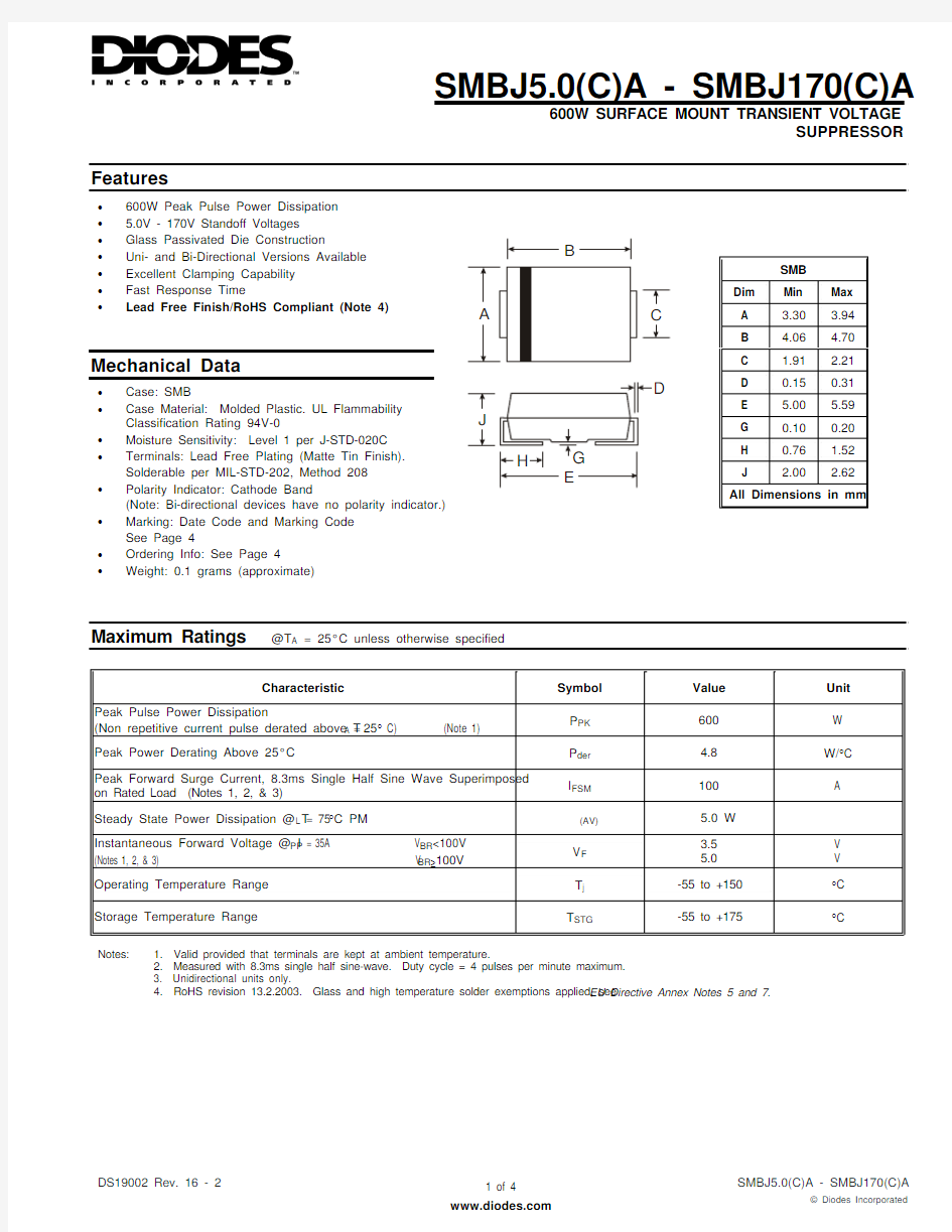
SMB
Dim Min Max A 3.30
3.94
B 4.06 4.70
C 1.91
2.21
D 0.15 0.31
E 5.00 5.59
G 0.10 0.20
H 0.76 1.52 J 2.00 2.62 All Dimensions in mm
Maximum Ratings @T A = 25°C unless otherwise specified
Characteristic Symbol Value Unit
Peak Pulse Power Dissipation
(Non repetitive current pulse derated above T A =25° C) (Note 1)
P PK600 W
Peak Power Derating Above 25°C P der 4.8 W/°C
Peak Forward Surge Current, 8.3ms Single Half Sine Wave Superimposed
on Rated Load (Notes 1, 2, & 3) I FSM
100 A
Steady State Power Dissipation @ T L = 75°C PM(AV) 5.0 W
Instantaneous Forward Voltage @ I PP = 35A V BR<100V (Notes 1, 2, & 3) V BR≥100V V F
3.5
5.0
V
V
Operating Temperature Range T j-55 to +150 °C Storage Temperature Range T STG-55 to +175 °C Notes: 1. Valid provided that terminals are kept at ambient temperature.
2. Measured with 8.3ms single half sine-wave. Duty cycle = 4 pulses per minute maximum.
3. Unidirectional units only.
4. RoHS revision 13.2.2003. Glass and high temperature solder exemptions applied, see EU Directive Annex Notes 5 and 7.
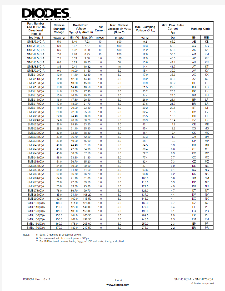
Part Number Add C For Bi-Directional (Note 5) Reverse Standoff Voltage Breakdown Voltage V BR @ I T (Note 6)Test
Current
Max. Reverse
Leakage @ V RWM
(Note 7) Max. Clamping Voltage @ I pp
Max. Peak Pulse
Current I pp
Marking Code See Note 4 V RWM (V) Min (V) Max (V)I T (mA) I R (μA) V C (V) (A) BI- UNI- SMBJ5.0(C)A 5.0 6.40 7.23 10 800 9.2 65.2 AE KE SMBJ6.0(C)A 6.0 6.67 7.67 10 800 10.3 58.3 AG KG SMBJ6.5(C)A 6.5 7.22 8.30 10 500 11.2 53.6 AK KK SMBJ7.0(C)A 7.0 7.78 8.95 10 200 12.0 50.0 AM KM SMBJ7.5(C)A 7.5 8.33 9.58 1.0 100 12.9 46.5 AP KP SMBJ8.0(C)A 8.0 8.89 10.23 1.0 50 13.6 44.1 AR KR SMBJ8.5(C)A 8.5 9.44 10.82 1.0 10 14.4 41.7 AT KT SMBJ9.0(C)A 9.0 10.00 11.50 1.0 5.0 15.4 39.0 AV KV SMBJ10(C)A 10.0 11.10 12.80 1.0 5.0 17.0 35.3 AX KX SMBJ11(C)A 11.0 12.20 14.40 1.0 5.0 18.2 33.0 AZ KZ SMBJ12(C)A 12.0 13.30 15.30 1.0 5.0 19.9 30.2 BE LE SMBJ13(C)A 13.0 14.40 16.50 1.0 5.0 21.5 27.9 BG LG SMBJ14(C)A 14.0 15.60 17.90 1.0 5.0 23.2 25.8 BK LK SMBJ15(C)A 15.0 16.70 19.20 1.0 5.0 24.4 24.0 BM LM SMBJ16(C)A 16.0 17.80 20.50 1.0 5.0 26.0 23.1 BP LP SMBJ17(C)A 17.0 18.90 21.70 1.0 5.0 27.6 21.7 BR LR SMBJ18(C)A 18.0 20.00 23.30 1.0 5.0 29.2 20.5 BT LT SMBJ20(C)A 20.0 22.20 25.50 1.0 5.0 32.4 18.5 BV LV SMBJ22(C)A 22.0 24.40 28.00 1.0 5.0 35.5 16.9 BX LX SMBJ24(C)A 24.0 26.70 30.70 1.0 5.0 38.9 15.4 BZ LZ SMBJ26(C)A 26.0 28.90 33.20 1.0 5.0 42.1 14.2 CE ME SMBJ28(C)A 28.0 31.10 35.80 1.0 5.0 45.4 13.2 CG MG SMBJ30(C)A 30.0 33.30 38.30 1.0 5.0 48.4 12.4 CK MK SMBJ33(C)A 33.0 36.70 42.20 1.0 5.0 53.3 11.3 CM MM SMBJ36(C)A 36.0 40.00 46.00 1.0 5.0 58.1 10.3 CP MP SMBJ40(C)A 40.0 44.40 51.10 1.0 5.0 64.5 9.3 CR MR SMBJ43(C)A 43.0 47.80 54.90 1.0 5.0 69.4 8.6 CT MT SMBJ45(C)A 45.0 50.00 57.50 1.0 5.0 72.7 8.3 CV MV SMBJ48(C)A 48.0 53.30 61.30 1.0 5.0 77.4 7.7 CX MX SMBJ51(C)A 51.0 56.70 65.20 1.0 5.0 82.4 7.3 CZ MZ SMBJ54(C)A 54.0 60.00 69.00 1.0 5.0 87.1 6.9 DE NE SMBJ58(C)A 58.0 64.40 74.60 1.0 5.0 93.6 6.4 DG NG SMBJ60(C)A 60.0 66.70 76.70 1.0 5.0 96.8 6.2 DK NK SMBJ64(C)A 64.0 71.10 81.80 1.0 5.0 103.0 5.8 DM NM SMBJ70(C)A 70.0 77.80 89.50 1.0 5.0 113.0 5.3 DP NP SMBJ75(C)A 75.0 83.30 95.80 1.0 5.0 121.0 4.9 DR NR SMBJ78(C)A 78.0 86.70 99.70 1.0 5.0 126.0 4.7 DT NT SMBJ85(C)A 85.0 94.40 108.20 1.0 5.0 137.0 4.4 DV NV SMBJ90(C)A 90.0 100.0 115.50 1.0 5.0 146.0 4.1 DX NX SMBJ100(C)A 100.0 111.0 128.00 1.0 5.0 162.0 3.7 DZ NZ SMBJ110(C)A 110.0 122.0 140.00 1.0 5.0 177.0 3.4 EE PE SMBJ120(C)A 120.0 133.0 153.00 1.0 5.0 193.0 3.1 EG PG SMBJ130(C)A 130.0 144.0 165.50 1.0 5.0 209.0 2.9 EK PK SMBJ150(C)A 150.0 167.0 192.50 1.0 5.0 243.0 2.5 EM PM SMBJ160(C)A 160.0 178.0 205.00 1.0 5.0 259.0 2.3 EP PP SMBJ170(C)A
170.0
189.0
217.50
1.0
5.0
275.0
2.2
ER
PR
Notes:
5. Suffix C denotes Bi-directional device.
6. V BR measured with I T current pulse = 300μs
7. For Bi-Directional devices having V RWM of 10V and under, the I R is doubled.
1
1010010
100
1000
10,000
V , REVERSE STANDOFF VOLTAGE (V)
Fig. 2 Typical T otal Capacitance
RWM 0
25
50
75
100
125
150
175200
10075
50
25
0T , AMBIENT TEMPERATURE (C)
Fig. 1 Pulse Derating Curve
A °P E A K P U L S E D E R A T I N G I N % O F P E A K P O W E R O R C U R R E N T
1000
C , C A P A C I T A N C E (p F )
T
0.1
1.0
0.1
10
100
1.0
10
1000
10000
P , P E A K P U L S E P O W E R (k W )
P K 100
I , P E A K P U L S E C U R R E N T (%I )
P P p
p t, TIME (ms)
Fig. 4 Pulse Waveform
0.0
1.0
2.0
3.0
25
50
75
100
125
150
175
200
P M
S T E A D Y S T A T E P O W E R D I S S I P A T I O N (W )
(A V ),T , LEAD TEMPERATURE (C)
Fig. 6 Steady State Power Derating Curve
L °4.0
5.0
12010080
60
40
20
2510I , P E A K F O R W A R D S U R G E C U R R E N T (A )
F S M NUMBER OF CYCLES AT 60Hz
Fig. 5 Maximum Non-Repetitive Surge Current
2050100
1
Ordering Information (Note 8)
Device*Packaging Shipping SMBJXXX(C)A-13-F SMB 3000/Tape & Reel
Notes: 8. For packaging details, visit our website at https://www.360docs.net/doc/1d14295645.html,/datasheets/ap02007.pdf.
*x = Device Voltage, e.g., SMBJ170A-13-F.
Marking Information
XX = Product type marking code (See Page 2)
YWW
= Manufacturers’ code marking
YWW = Date code marking
Y = Last digit of year ex: 2 for 2002
WW = Week code 01 to 52
IMPORTANT NOTICE
Diodes Incorporated and its subsidiaries reserve the right to make modifications, enhancements, improvements, corrections or other changes without further notice to any product herein. Diodes Incorporated does not assume any liability arising out of the application or use of any product described herein; neither does it convey any license under its patent rights, nor the rights of others. The user of products in such applications shall assume all risks of such use and will agree to hold Diodes Incorporated and all the companies whose products are represented on our website, harmless against all damages.
LIFE SUPPORT
Diodes Incorporated products are not authorized for use as critical components in life support devices or systems without the expressed written approval of the President of Diodes Incorporated.