tl431详细英文数据手册

1
2
3
4
8
7
6
5
CATHODE
ANODE
ANODE
NC
REF
ANODE
ANODE
NC
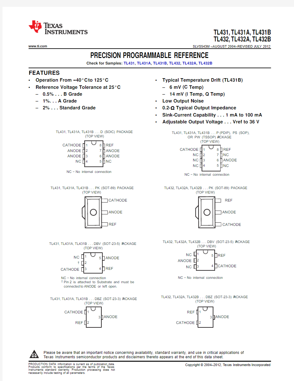
TL431,TL431A,TL431B...D (SOIC) PACKAGE
(TOP VIEW)
1
2
3
4
8
7
6
5
CATHODE
NC
NC
NC
REF
NC
ANODE
NC
TL431,TL431A,TL431B...P(PDIP), PS (SOP),
OR PW (TSSOP) P ACKAGE
(TOP VIEW)
NC?No internal connection
TL431,TL431A,TL431B...DBV (SOT-23-5) P ACKAGE
(TOP VIEW)
1
2
3
5
4
NC
?
CATHODE
ANODE
REF
TL431,TL431A,TL431B...PK (SOT-89) PACKAGE
(TOP VIEW)
REF
ANODE
CATHODE
?Pin2 is attached to Substrate and must be
connected to ANODE or left open.
NC?No internal connection
TL432,TL432A,TL432B...DBV (SOT-23-5) P ACKAGE
(TOP VIEW)
1
2
3
5
4
NC
ANODE
NC
REF
CATHODE
NC?No internal connection
TL431,TL431A,TL431B...DBZ (SOT-23-3) P ACKAGE
(TOP VIEW)
TL432,TL432A,TL432B...DBZ (SOT-23-3) P ACKAGE
(TOP VIEW)
NC?No internal connection
1
2
3
REF
CATHODE
ANODE
1
2
3
CATHODE
REF
ANODE
A
N
O
D
E
TL432,TL432A,TL432B...PK (SOT-89) PACKAGE
(TOP VIEW)
REF
ANODE
CATHODE
A
N
O
D
E
TL431,TL431A,TL431B
TL432,TL432A,TL432B https://www.360docs.net/doc/1314600833.html, SLVS543M–AUGUST2004–REVISED JULY2012
PRECISION PROGRAMMABLE REFERENCE
Check for Samples:TL431,TL431A,TL431B,TL432,TL432A,TL432B
FEATURES
?Operation From?40°C to125°C?Typical Temperature Drift(TL431B)?Reference Voltage Tolerance at25°C–6mV(C Temp)
–0.5%...B Grade–14mV(I Temp,Q Temp)
–1%...A Grade?Low Output Noise
–2%...Standard Grade?0.2-ΩTypical Output Impedance
?Sink-Current Capability...1mA to100mA
?Adjustable Output Voltage...Vref to36V
Please be aware that an important notice concerning availability,standard warranty,and use in critical applications of
Texas Instruments semiconductor products and disclaimers thereto appears at the end of this data sheet.
PRODUCTION DATA information is current as of publication date.Copyright?2004–2012,Texas Instruments Incorporated Products conform to specifications per the terms of the Texas
CATHODE ANODE REF
TL431...KTP (PowerFLEX /TO-252) P ACKAGE
(TOP VIEW)
A N O D E
TL431A,TL431B ...DCK (SC-70) PACKAGE
(TOP VIEW)
123
654
CATHODE
NC REF
ANODE NC NC
NC ?No internal connection
TL431,TL431A,TL431B ...LP (TO-92/TO-226) P ACKAGE
(TOP VIEW)
CATHODE ANODE REF
TL431,TL431A,TL431B TL432,TL432A,TL432B
SLVS543M –AUGUST 2004–REVISED JULY 2012
https://www.360docs.net/doc/1314600833.html,
DESCRIPTION/ORDERING INFORMATION
The TL431and TL432are three-terminal adjustable shunt regulators,with specified thermal stability over applicable automotive,commercial,and military temperature ranges.The output voltage can be set to any value between Vref (approximately 2.5V)and 36V,with two external resistors (see Figure 17).These devices have a typical output impedance of 0.2Ω.Active output circuitry provides a very sharp turn-on characteristic,making these devices excellent replacements for Zener diodes in many applications,such as onboard regulation,adjustable power supplies,and switching power supplies.The TL432has exactly the same functionality and electrical specifications as the TL431,but has different pinouts for the DBV,DBZ,and PK packages.
Both the TL431and TL432devices are offered in three grades,with initial tolerances (at 25°C)of 0.5%,1%,and 2%,for the B,A,and standard grade,respectively.In addition,low output drift vs temperature ensures good stability over the entire temperature range.
The TL43xxC devices are characterized for operation from 0°C to 70°C,the TL43xxI devices are characterized for operation from –40°C to 85°C,and the TL43xxQ devices are characterized for operation from –40°C to 125°C.
2Submit Documentation Feedback Copyright ?2004–2012,Texas Instruments Incorporated
TL431,TL431A,TL431B
TL432,TL432A,TL432B https://www.360docs.net/doc/1314600833.html, SLVS543M–AUGUST2004–REVISED JULY2012
V ref TOLERANCE(25°C)=2%
TL431,TL432ORDERING INFORMATION(1)
TOP-SIDE T A PACKAGE(2)ORDERABLE PART NUMBER
MARKING(3) PDIP(P)Tube of50TL431CP TL431CP
Tube of75TL431CD
SOIC(D)TL431C
Reel of2500TL431CDR
SOP(PS)Reel of2000TL431CPSR T431
Reel of3000TL431CDBVR
T3C_
Reel of250TL431CDBVT
SOT-23-5(DBV)
Reel of3000TL432CDBVR
T4C_
Reel of250TL432CDBVT
Reel of3000TL431CDBZR
T3C_ 0°C to70°C Reel of250TL431CDBZT
SOT-23-3(DBZ)
Reel of3000TL432CDBZR
T4C_
Reel of250TL432CDBZT
TL431CPK43
SOT-89(PK)Reel of1000
TL432CPK2A
Bulk of1000,straight lead TL431CLP
TO-226/TO-92(LP)Ammo of2000,formed lead TL431CLPM TL431C
Reel of2000,formed lead TL431CLPR
Tube of150TL431CPW
TSSOP(PW)T431
Reel of2000TL431CPWR
PDIP(P)Tube of50TL431IP TL431IP
Tube of75TL431ID
SOIC(D)TL431I
Reel of2500TL431IDR
Reel of3000TL431IDBVR
T3I_
Reel of250TL431IDBVT
SOT-23-5(DBV)
Reel of3000TL432IDBVR
T4I_
Reel of250TL432IDBVT
Reel of3000TL431IDBZR
-40°C to85°C T3I_
Reel of250TL431IDBZT
SOT-23-3(DBZ)
Reel of3000TL432IDBZR
T4I_
Reel of250TL432IDBZT
TL431IPK3I
SOT-89(PK)Reel of1000
TL432IPK2B
Bulk of1000,straight lead TL431ILP
TO-226/TO-92(LP)Ammo of2000,formed lead TL431ILPM TL431I
Reel of2000,formed lead TL431ILPR
(1)For the most current package and ordering information,see the Package Option Addendum at the end of this document,or see the TI
web site at https://www.360docs.net/doc/1314600833.html,.
(2)Package drawings,thermal data,and symbolization are available at https://www.360docs.net/doc/1314600833.html,/packaging.
(3)DBV/DBZ/DCK:The actual top-side marking has one additional character that designates the wafer fab/assembly site.
Copyright?2004–2012,Texas Instruments Incorporated Submit Documentation Feedback3
TL431,TL431A,TL431B
TL432,TL432A,TL432B
SLVS543M–AUGUST2004–REVISED https://www.360docs.net/doc/1314600833.html,
V ref TOLERANCE(25°C)=2%
TL431,TL432ORDERING INFORMATION(1)(continued)
TOP-SIDE T A PACKAGE(2)ORDERABLE PART NUMBER
MARKING(3)
Reel of3000TL431QDBVR
T3Q_
Reel of250TL431QDBVT
SOT-23-5(DBV)
Reel of3000TL432QDBVR
T4Q_
Reel of250TL432QDBVT
Reel of3000TL431QDBZR
T3Q_
Reel of250TL431QDBZT
-40°C to125°C SOT-23-3(DBZ)
Reel of3000TL432QDBZR
T4Q_
Reel of250TL432QDBZT
TL431QPK3Q
SOT-89(PK)Reel of1000
TL432QPK2C
Reel of1000TL431QDCKR
SC-70(DCK)T6_
Reel of250TL431QDCKT
4Submit Documentation Feedback Copyright?2004–2012,Texas Instruments Incorporated
TL431,TL431A,TL431B
TL432,TL432A,TL432B https://www.360docs.net/doc/1314600833.html, SLVS543M–AUGUST2004–REVISED JULY2012
V ref TOLERANCE(25°C)=1%
TL431A,TL432A ORDERING INFORMATION(1)
TOP-SIDE T A PACKAGE(2)ORDERABLE PART NUMBER
MARKING(3) PDIP(P)Tube of50TL431ACP TL431ACP
SC-70(DCK)Reel of3000TL431ACDCKR T4_
Reel of250TL431ACDCKT
SOIC(D)Tube of75TL431ACD431AC
Reel of2500TL431ACDR
SOP(PS)Reel of2000TL431ACPSR T431A
SOT-23-5(DBV)Reel of3000TL431ACDBVR TAC_
Reel of250TL431ACDBVT
Reel of3000TL432ACDBVR T4B_
Reel of250TL432ACDBVT
SOT-23-3(DBZ)Reel of3000TL431ACDBZR TAC_ 0°C to70°C
Reel of250TL431ACDBZT
Reel of3000TL432ACDBZR T4B_
Reel of250TL432ACDBZT
SOT-89(PK)Reel of1000TL431ACPK4A
TL432ACPK2D
TO-226/TO-92(LP)Bulk of1000,straight lead TL431ACLP TL431AC
Ammo of2000,formed lead TL431ACLPM
Reel of2000,formed lead TL431ACLPR
Reel of2000,formed lead TL431ACLPRE3
TSSOP(PW)Tube of150TL431ACPW T431A
Reel of2000TL431ACPWR
PDIP(P)Tube of50TL431AIP TL431AIP
SC-70(DCK)Reel of3000TL431AIDCKR T5_
Reel of250TL431AIDCKT
SOIC(D)Tube of75TL431AID431AI
Reel of2500TL431AIDR
SOT-23-5(DBV)Reel of3000TL431AIDBVR TAI_
Reel of250TL431AIDBVT
Reel of3000TL432AIDBVR T4A_
Reel of250TL432AIDBVT
-40°C to85°C
SOT-23-3(DBZ)Reel of3000TL431AIDBZR TAI_
Reel of250TL431AIDBZT
Reel of3000TL432AIDBZR T4A_
Reel of250TL432AIDBZT
SOT-89(PK)Reel of1000TL431AIPK4B
TL432AIPK2E
TO-226/TO-92(LP)Bulk of1000,straight lead TL431AILP TL431AI
Ammo of2000,formed lead TL431AILPM
Reel of2000,formed lead TL431AILPR
(1)For the most current package and ordering information,see the Package Option Addendum at the end of this document,or see the TI
web site at https://www.360docs.net/doc/1314600833.html,.
(2)Package drawings,thermal data,and symbolization are available at https://www.360docs.net/doc/1314600833.html,/packaging.
(3)DBV/DBZ/DCK:The actual top-side marking has one additional character that designates the wafer fab/assembly site.
Copyright?2004–2012,Texas Instruments Incorporated Submit Documentation Feedback5
TL431,TL431A,TL431B
TL432,TL432A,TL432B
SLVS543M–AUGUST2004–REVISED https://www.360docs.net/doc/1314600833.html,
V ref TOLERANCE(25°C)=1%
TL431A,TL432A ORDERING INFORMATION(1)(continued)
TOP-SIDE T A PACKAGE(2)ORDERABLE PART NUMBER
MARKING(3) SOT-23-5(DBV)Reel of3000TL431AQDBVR TAQ_
Reel of250TL431AQDBVT
Reel of3000TL432AQDBVR T4D_
Reel of250TL432AQDBVT
SOT-23-3(DBZ)Reel of3000TL431AQDBZR TAQ_
Reel of250TL431AQDBZT
-40°C to125°C
Reel of3000TL432AQDBZR T4D_
Reel of250TL432AQDBZT
SOT-89(PK)Reel of1000TL431AQPK4D
TL432AQPK2F
SC-70(PK)Reel of1000TL431AQDCKR T7_
Reel of250TL431AQDCKT
6Submit Documentation Feedback Copyright?2004–2012,Texas Instruments Incorporated
TL431,TL431A,TL431B
TL432,TL432A,TL432B https://www.360docs.net/doc/1314600833.html, SLVS543M–AUGUST2004–REVISED JULY2012
V ref TOLERANCE(25°C)=0.5%
TL431B,TL432B ORDERING INFORMATION(1)
TOP-SIDE T A PACKAGE(2)ORDERABLE PART NUMBER
MARKING(3) PDIP(P)Tube of50TL431BCP TL431BCP
SC-70(DCK)Reel of3000TL431BCDCKR T2_
Reel of250TL431BCDCKT
SOIC(D)Tube of75TL431BCD T431B
Reel of2500TL431BCDR
SOP(PS)Reel of2000TL431BCPSR TL431B
SOT-23-5(DBV)Reel of3000TL431BCDBVR T3G_
Reel of250TL431BCDBVT
Reel of3000TL432BCDBVR TBC_
Reel of250TL432BCDBVT
0°C to70°C SOT-23-3(DBZ)Reel of3000TL431BCDBZR T3G_
Reel of250TL431BCDBZT
Reel of3000TL432BCDBZR TBC_
Reel of250TL432BCDBZT
SOT-89(PK)Reel of1000TL431BCPK4C
TL432BCPK2G
TO-226/TO-92(LP)Bulk of1000,straight lead TL431BCLP TL431B
Ammo of2000,formed lead TL431BCLPM
Reel of2000,formed lead TL431BCLPR
TSSOP(PW)Tube of150TL431BCPW T431B
Reel of2000TL431BCPWR
PDIP(P)Tube of50TL431BIP TL431BIP
SC-70(DCK)Reel of3000TL431BIDCKR T3_
Reel of250TL431BIDCKT
SOIC(D)Tube of75TL431BID Z431B
Reel of2500TL431BIDR
SOT-23-5(DBV)Reel of3000TL431BIDBVR T3F_
Reel of250TL431BIDBVT
Reel of3000TL432BIDBVR T4F_
Reel of250TL432BIDBVT
-40°C to85°C
SOT-23-3(DBZ)Reel of3000TL431BIDBZR T3F_
Reel of250TL431BIDBZT
Reel of3000TL432BIDBZR T4F_
Reel of250TL432BIDBZT
SOT-89(PK)Reel of1000TL431BIPK4I
TL432BIPK2H
TO-226/TO-92(LP)Bulk of1000,straight lead TL431BILP Z431B
Ammo of2000,formed lead TL431BILPM
Reel of2000,formed lead TL431BILPR
(1)For the most current package and ordering information,see the Package Option Addendum at the end of this document,or see the TI
web site at https://www.360docs.net/doc/1314600833.html,.
(2)Package drawings,thermal data,and symbolization are available at https://www.360docs.net/doc/1314600833.html,/packaging.
(3)DBV/DBZ/DCK:The actual top-side marking has one additional character that designates the wafer fab/assembly site.
Copyright?2004–2012,Texas Instruments Incorporated Submit Documentation Feedback7
TL431,TL431A,TL431B
TL432,TL432A,TL432B
SLVS543M–AUGUST2004–REVISED https://www.360docs.net/doc/1314600833.html,
V ref TOLERANCE(25°C)=0.5%
TL431B,TL432B ORDERING INFORMATION(1)(continued)
TOP-SIDE T A PACKAGE(2)ORDERABLE PART NUMBER
MARKING(3) SOIC(D)Tube of75TL431BQD T431BQ
Reel of2500TL431BQDR
SOT-23-5(DBV)Reel of3000TL431BQDBVR T3H_
Reel of250TL431BQDBVT
Reel of3000TL432BQDBVR T4H_
Reel of250TL432BQDBVT
SOT-23-3(DBZ)Reel of3000TL431BQDBZR T3H_
Reel of250TL431BQDBZT
-40°C to125°C Reel of3000TL432BQDBZR T4H_
Reel of250TL432BQDBZT
SOT-89(PK)Reel of1000TL431BQPK3H
TL432BQPK2J
TO-226/TO-92(LP)Bulk of1000,straight lead TL431BQLP T431BQ
Ammo of2000,formed lead TL431BQLPM
Reel of2000,formed lead TL431BQLPR
SC-70(DCK)Reel of1000TL431BQDCKR T8_
Reel of250TL431BQDCKT
8Submit Documentation Feedback Copyright?2004–2012,Texas Instruments Incorporated
ANODE
REF
CATHODE
ANODE
REF
CATHODE
ANODE
TL431,TL431A,TL431B TL432,TL432A,TL432B
https://www.360docs.net/doc/1314600833.html,
SLVS543M –AUGUST 2004–REVISED JULY 2012
Figure 1.SYMBOL
Figure 2.FUNCTIONAL BLOCK DIAGRAM
Figure 3.EQUIVALENT SCHEMATIC
NOTE:All component values are nominal.
Copyright ?2004–2012,Texas Instruments Incorporated Submit Documentation Feedback 9
TL431,TL431A,TL431B
TL432,TL432A,TL432B
SLVS543M–AUGUST2004–REVISED https://www.360docs.net/doc/1314600833.html, ABSOLUTE MAXIMUM RATINGS(1)
over operating free-air temperature range(unless otherwise noted)
MIN MAX UNIT
V KA Cathode voltage(2)37V
I KA Continuous cathode current range–100150mA
I I(ref)Reference input current range–0.0510mA
T J Operating virtual junction temperature150°C
T stg Storage temperature range–65150°C (1)Stresses beyond those listed under"absolute maximum ratings"may cause permanent damage to the device.These are stress ratings
only,and functional operation of the device at these or any other conditions beyond those indicated under"recommended operating conditions"is not implied.Exposure to absolute-maximum-rated conditions for extended periods may affect device reliability.
(2)All voltage values are with respect to ANODE,unless otherwise noted.
PACKAGE THERMAL DATA(1)
PACKAGE BOARDθJCθJA
PDIP(P)High K,JESD51-757°C/W85°C/W
SC-70(DCK)High K,JESD51-7259°C/W87°C/W
SOIC(D)High K,JESD51-739°C/W97°C/W
SOP(PS)High K,JESD51-746°C/W95°C/W
SOT-89(PK)High K,JESD51-79°C/W52°C/W
SOT-23-5(DBV)High K,JESD51-7131°C/W206°C/W
SOT-23-3(DBZ)High K,JESD51-776°C/W206°C/W TO-92(LP)High K,JESD51-755°C/W140°C/W
TSSOP(PW)High K,JESD51-765°C/W149°C/W
(1)Maximum power dissipation is a function of T J(max),θJA,and T A.The maximum allowable power dissipation at any allowable ambient
temperature is P D=(T J(max)–T A)/θJA.Operating at the absolute maximum T J of150°C can affect reliability. RECOMMENDED OPERATING CONDITIONS
MIN MAX UNIT
V KA Cathode voltage V ref36V
I KA Cathode current1100mA
TL43xxC070
T A Operating free-air temperature TL43xxI–4085°C
TL43xxQ–40125
10Submit Documentation Feedback Copyright?2004–2012,Texas Instruments Incorporated
R2R1|z |KA (
1 +
?I ?V
|z'| =?I KA
?V KA
|z | =
KA (2)
The dynamic impedance is defined as:
When the device is operating with two external resistors (see Figure 5),the total dynamic impedance of the circuit is given by:
which is approximately equal to
.TL431,TL431A,TL431B TL432,TL432A,TL432B
https://www.360docs.net/doc/1314600833.html,
SLVS543M –AUGUST 2004–REVISED JULY 2012
ELECTRICAL CHARACTERISTICS
over recommended operating conditions,T A =25°C (unless otherwise noted)
TL431C,TL432C PARAMETER
TEST CIRCUIT
TEST CONDITIONS
UNIT MIN TYP MAX V ref Reference voltage
Figure 4V KA =V ref ,I KA =10mA 2440
2495
2550mV SOT23-3and TL432Deviation of reference input 616V KA =V ref ,devices V I(dev)voltage over full temperature Figure 4
mV
I KA =10mA,range (1)
All other devices 425Ratio of change in reference ΔV KA =10V ?V ref -1.4-2.7ΔV ref /voltage to the change in Figure 5I KA =10mA
mV/V ΔV KA ΔV KA =36V ?10V
-1-2cathode voltage I ref Reference input current Figure 5I KA =10mA,R1=10k ?,R2=∞24μA Deviation of reference input I I(dev)current over full temperature Figure 5I KA =10mA,R1=10k ?,R2=∞0.4 1.2μA range (1)
Minimum cathode current for I min Figure 4V KA =V ref
0.41mA regulation
I off Off-state cathode current Figure 6V KA =36V,V ref =0
0.11μA |z KA |Dynamic impedance (2)
Figure 4
V KA =V ref ,f ≤1kHz,I KA =1mA to 100mA
0.2
0.5
?(1)
The deviation parameters V ref(dev)and I ref(dev)are defined as the differences between the maximum and minimum values obtained over the rated average full-range αVref is positive or negative,depending on whether minimum V ref or maximum V ref ,respectively,occurs at the lower temperature.
Copyright ?2004–2012,Texas Instruments Incorporated Submit Documentation Feedback 11
R2R1|z |KA (
1 +
?I ?V
|z'| =?I KA
?V KA
|z | =
KA (2)
The dynamic impedance is defined as:
When the device is operating with two external resistors (see Figure 5),the total dynamic impedance of the circuit is given by:
which is approximately equal to
.TL431,TL431A,TL431B TL432,TL432A,TL432B
SLVS543M –AUGUST 2004–REVISED JULY 2012
https://www.360docs.net/doc/1314600833.html,
ELECTRICAL CHARACTERISTICS
over recommended operating conditions,T A =25°C (unless otherwise noted)
TL431I,TL432I PARAMETER
TEST CIRCUIT
TEST CONDITIONS
UNIT MIN TYP MAX V ref Reference voltage
Figure 4V KA =V ref ,I KA =10mA 2440
24952550mV SOT23-3and TL432Deviation of reference input 1434V KA =V ref ,devices V I(dev)voltage over full temperature Figure 4
mV
I KA =10mA range (1)
All other devices 550Ratio of change in reference ΔV KA =10V ?V ref -1.4-2.7ΔV ref /voltage to the change in Figure 5I KA =10mA
mV/V ΔV KA ΔV KA =36V ?10V
-1-2cathode voltage I ref Reference input current Figure 5I KA =10mA,R1=10k ?,R2=∞24μA Deviation of reference input I I(dev)current over full temperature Figure 5I KA =10mA,R1=10k ?,R2=∞0.8 2.5μA range (1)
Minimum cathode current for I min Figure 4V KA =V ref
0.41mA regulation
I off Off-state cathode current Figure 6V KA =36V,V ref =0
0.11μA |z KA |Dynamic impedance (2)
Figure 4
V KA =V ref ,f ≤1kHz,I KA =1mA to 100mA
0.2
0.5
?(1)
The deviation parameters V ref(dev)and I ref(dev)are defined as the differences between the maximum and minimum values obtained over the rated average full-range αVref is positive or negative,depending on whether minimum V ref or maximum V ref ,respectively,occurs at the lower temperature.
12Submit Documentation Feedback Copyright ?2004–2012,Texas Instruments Incorporated
R2R1|z |KA (
1 +
?I ?V
|z'| =?I KA
?V KA
|z | =
KA (2)
The dynamic impedance is defined as:
When the device is operating with two external resistors (see Figure 5),the total dynamic impedance of the circuit is given by:
which is approximately equal to
.TL431,TL431A,TL431B TL432,TL432A,TL432B
https://www.360docs.net/doc/1314600833.html,
SLVS543M –AUGUST 2004–REVISED JULY 2012
ELECTRICAL CHARACTERISTICS
over recommended operating conditions,T A =25°C (unless otherwise noted)
TL431Q,TL432Q PARAMETER
TEST CIRCUIT
TEST CONDITIONS
UNIT MIN TYP MAX V ref Reference voltage
Figure 4V KA =V ref ,I KA =10mA 2440
24952550mV Deviation of reference input V I(dev)voltage over full temperature Figure 4
V KA =V ref ,I KA =10mA
1434mV
range (1)
Ratio of change in reference ΔV KA =10V ?V ref -1.4-2.7ΔV ref /voltage to the change in Figure 5I KA =10mA
mV/V ΔV KA ΔV KA =36V ?10V
-1-2cathode voltage I ref Reference input current Figure 5I KA =10mA,R1=10k ?,R2=∞24μA Deviation of reference input I I(dev)current over full temperature Figure 5I KA =10mA,R1=10k ?,R2=∞0.8 2.5μA range (1)
Minimum cathode current for I min Figure 4V KA =V ref
0.41mA regulation
I off Off-state cathode current Figure 6V KA =36V,V ref =0
0.11μA |z KA |Dynamic impedance (2)
Figure 4
V KA =V ref ,f ≤1kHz,I KA =1mA to 100mA
0.2
0.5
?(1)
The deviation parameters V ref(dev)and I ref(dev)are defined as the differences between the maximum and minimum values obtained over the rated full-range αVref is positive or negative,depending on whether minimum V ref or maximum V ref ,respectively,occurs at the lower temperature.
Copyright ?2004–2012,Texas Instruments Incorporated Submit Documentation Feedback 13
R2R1|z |KA (
1 +
?I ?V
|z'| =?I KA
?V KA
|z | =
KA (2)
The dynamic impedance is defined as:
When the device is operating with two external resistors (see Figure 5),the total dynamic impedance of the circuit is given by:
which is approximately equal to
.TL431,TL431A,TL431B TL432,TL432A,TL432B
SLVS543M –AUGUST 2004–REVISED JULY 2012
https://www.360docs.net/doc/1314600833.html,
ELECTRICAL CHARACTERISTICS
over recommended operating conditions,T A =25°C (unless otherwise noted)
TL431AC,TL432AC PARAMETER
TEST CIRCUIT
TEST CONDITIONS
UNIT MIN TYP MAX V ref Reference voltage
Figure 4V KA =V ref ,I KA =10mA 2470
2495
2520mV SOT23-3and TL432Deviation of reference input 616V KA =V ref ,devices V I(dev)voltage over full temperature Figure 4
mV
I KA =10mA range (1)
All other devices 425Ratio of change in reference ΔV KA =10V ?V ref -1.4-2.7ΔV ref /voltage to the change in Figure 5I KA =10mA
mV/V ΔV KA ΔV KA =36V ?10V
-1-2cathode voltage I ref Reference input current Figure 5I KA =10mA,R1=10k ?,R2=∞24μA Deviation of reference input I I(dev)current over full temperature Figure 5I KA =10mA,R1=10k ?,R2=∞0.8 1.2μA range (1)
Minimum cathode current for I min Figure 4V KA =V ref
0.40.6mA regulation
I off Off-state cathode current Figure 6V KA =36V,V ref =0
0.10.5μA |z KA |Dynamic impedance (2)
Figure 4
V KA =V ref ,f ≤1kHz,I KA =1mA to 100mA
0.2
0.5
?(1)
The deviation parameters V ref(dev)and I ref(dev)are defined as the differences between the maximum and minimum values obtained over the rated average full-range αVref is positive or negative,depending on whether minimum V ref or maximum V ref ,respectively,occurs at the lower temperature.
14Submit Documentation Feedback Copyright ?2004–2012,Texas Instruments Incorporated
R2R1|z |KA (
1 +
?I ?V
|z'| =?I KA
?V KA
|z | =
KA (2)
The dynamic impedance is defined as:
When the device is operating with two external resistors (see Figure 5),the total dynamic impedance of the circuit is given by:
which is approximately equal to
.TL431,TL431A,TL431B TL432,TL432A,TL432B
https://www.360docs.net/doc/1314600833.html,
SLVS543M –AUGUST 2004–REVISED JULY 2012
ELECTRICAL CHARACTERISTICS
over recommended operating conditions,T A =25°C (unless otherwise noted)
TL431AI,TL432AI PARAMETER
TEST CIRCUIT
TEST CONDITIONS
UNIT MIN TYP MAX V ref Reference voltage
Figure 4V KA =V ref ,I KA =10mA 2470
24952520mV SOT23-3and TL432Deviation of reference input 1434V KA =V ref ,devices V I(dev)voltage over full temperature Figure 4
mV
I KA =10mA range (1)
All other devices 550Ratio of change in reference ΔV KA =10V ?V ref -1.4-2.7ΔV ref /voltage to the change in Figure 5I KA =10mA
mV/V ΔV KA ΔV KA =36V ?10V
-1-2cathode voltage I ref Reference input current Figure 5I KA =10mA,R1=10k ?,R2=∞24μA Deviation of reference input I I(dev)current over full temperature Figure 5I KA =10mA,R1=10k ?,R2=∞0.8 2.5μA range (1)
Minimum cathode current for I min Figure 4V KA =V ref
0.40.7mA regulation
I off Off-state cathode current Figure 6V KA =36V,V ref =0
0.10.5μA |z KA |Dynamic impedance (2)
Figure 4
V KA =V ref ,f ≤1kHz,I KA =1mA to 100mA
0.2
0.5
?(1)
The deviation parameters V ref(dev)and I ref(dev)are defined as the differences between the maximum and minimum values obtained over the rated average full-range αVref is positive or negative,depending on whether minimum V ref or maximum V ref ,respectively,occurs at the lower temperature.
Copyright ?2004–2012,Texas Instruments Incorporated Submit Documentation Feedback 15
R2R1|z |KA (
1 +
?I ?V
|z'| =?I KA
?V KA
|z | =
KA (2)
The dynamic impedance is defined as:
When the device is operating with two external resistors (see Figure 5),the total dynamic impedance of the circuit is given by:
which is approximately equal to
.TL431,TL431A,TL431B TL432,TL432A,TL432B
SLVS543M –AUGUST 2004–REVISED JULY 2012
https://www.360docs.net/doc/1314600833.html,
ELECTRICAL CHARACTERISTICS
over recommended operating conditions,T A =25°C (unless otherwise noted)
TL431AQ,TL432AQ PARAMETER
TEST CIRCUIT
TEST CONDITIONS
UNIT MIN TYP MAX V ref Reference voltage
Figure 4V KA =V ref ,I KA =10mA 2470
24952520mV Deviation of reference input V I(dev)voltage over full temperature Figure 4
V KA =V ref ,I KA =10mA
1434mV
range (1)
Ratio of change in reference ΔV KA =10V ?V ref -1.4-2.7ΔV ref /voltage to the change in Figure 5I KA =10mA
mV/V ΔV KA ΔV KA =36V ?10V
-1-2cathode voltage I ref Reference input current Figure 5I KA =10mA,R1=10k ?,R2=∞24μA Deviation of reference input I I(dev)current over full temperature Figure 5I KA =10mA,R1=10k ?,R2=∞0.8 2.5μA range (1)
Minimum cathode current for I min Figure 4V KA =V ref
0.40.7mA regulation
I off Off-state cathode current Figure 6V KA =36V,V ref =0
0.10.5μA |z KA |Dynamic impedance (2)
Figure 4
V KA =V ref ,f ≤1kHz,I KA =1mA to 100mA
0.2
0.5
?(1)
The deviation parameters V ref(dev)and I ref(dev)are defined as the differences between the maximum and minimum values obtained over the rated full-range αVref is positive or negative,depending on whether minimum V ref or maximum V ref ,respectively,occurs at the lower temperature.
16Submit Documentation Feedback Copyright ?2004–2012,Texas Instruments Incorporated
R2R1|z |KA (
1 +
?I ?V
|z'| =?I KA
?V KA
|z | =
KA (2)
The dynamic impedance is defined as:
When the device is operating with two external resistors (see Figure 5),the total dynamic impedance of the circuit is given by:
which is approximately equal to
.TL431,TL431A,TL431B TL432,TL432A,TL432B
https://www.360docs.net/doc/1314600833.html,
SLVS543M –AUGUST 2004–REVISED JULY 2012
ELECTRICAL CHARACTERISTICS
over recommended operating conditions,T A =25°C (unless otherwise noted)
TL431BC,TL432BC PARAMETER
TEST CIRCUIT
TEST CONDITIONS
UNIT MIN TYP MAX V ref Reference voltage
Figure 4V KA =V ref ,I KA =10mA 2483
2495
2507mV Deviation of reference input V I(dev)voltage over full temperature Figure 4
V KA =V ref ,I KA =10mA
616mV
range (1)
Ratio of change in reference ΔV KA =10V ?V ref -1.4-2.7ΔV ref /voltage to the change in Figure 5I KA =10mA
mV/V ΔV KA ΔV KA =36V ?10V
-1-2cathode voltage I ref Reference input current Figure 5I KA =10mA,R1=10k ?,R2=∞24μA Deviation of reference input I I(dev)current over full temperature Figure 5I KA =10mA,R1=10k ?,R2=∞0.8 1.2μA range (1)
Minimum cathode current for I min Figure 4V KA =V ref
0.40.6mA regulation
I off Off-state cathode current Figure 6V KA =36V,V ref =0
0.10.5μA |z KA |Dynamic impedance (2)
Figure 4
V KA =V ref ,f ≤1kHz,I KA =1mA to 100mA
0.2
0.5
?(1)
The deviation parameters V ref(dev)and I ref(dev)are defined as the differences between the maximum and minimum values obtained over the rated full-range αVref is positive or negative,depending on whether minimum V ref or maximum V ref ,respectively,occurs at the lower temperature.
Copyright ?2004–2012,Texas Instruments Incorporated Submit Documentation Feedback 17
R2R1|z |KA (
1 +
?I ?V
|z'| =?I KA
?V KA
|z | =
KA (2)
The dynamic impedance is defined as:
When the device is operating with two external resistors (see Figure 5),the total dynamic impedance of the circuit is given by:
which is approximately equal to
.TL431,TL431A,TL431B TL432,TL432A,TL432B
SLVS543M –AUGUST 2004–REVISED JULY 2012
https://www.360docs.net/doc/1314600833.html,
ELECTRICAL CHARACTERISTICS
over recommended operating conditions,T A =25°C (unless otherwise noted)
TL431BI,TL432BI PARAMETER
TEST CIRCUIT
TEST CONDITIONS
UNIT MIN TYP MAX V ref Reference voltage
Figure 4V KA =V ref ,I KA =10mA 2483
24952507mV Deviation of reference input V I(dev)voltage over full temperature Figure 4
V KA =V ref ,I KA =10mA
1434mV
range (1)
Ratio of change in reference ΔV KA =10V ?V ref -1.4-2.7ΔV ref /voltage to the change in Figure 5I KA =10mA
mV/V ΔV KA ΔV KA =36V ?10V
-1-2cathode voltage I ref Reference input current Figure 5I KA =10mA,R1=10k ?,R2=∞24μA Deviation of reference input I I(dev)current over full temperature Figure 5I KA =10mA,R1=10k ?,R2=∞0.8 2.5μA range (1)
Minimum cathode current for I min Figure 4V KA =V ref
0.40.7mA regulation
I off Off-state cathode current Figure 6V KA =36V,V ref =0
0.10.5μA |z KA |Dynamic impedance (2)
Figure 4
V KA =V ref ,f ≤1kHz,I KA =1mA to 100mA
0.2
0.5
?(1)
The deviation parameters V ref(dev)and I ref(dev)are defined as the differences between the maximum and minimum values obtained over the rated full-range αVref is positive or negative,depending on whether minimum V ref or maximum V ref ,respectively,occurs at the lower temperature.
18Submit Documentation Feedback Copyright ?2004–2012,Texas Instruments Incorporated
R2R1|z |KA (
1 +
?I ?V
|z'| =?I KA
?V KA
|z | =
KA (2)
The dynamic impedance is defined as:
When the device is operating with two external resistors (see Figure 5),the total dynamic impedance of the circuit is given by:
which is approximately equal to
.TL431,TL431A,TL431B TL432,TL432A,TL432B
https://www.360docs.net/doc/1314600833.html,
SLVS543M –AUGUST 2004–REVISED JULY 2012
ELECTRICAL CHARACTERISTICS
over recommended operating conditions,T A =25°C (unless otherwise noted)
TL431BQ,TL432BQ PARAMETER
TEST CIRCUIT
TEST CONDITIONS
UNIT MIN TYP MAX V ref Reference voltage
Figure 4V KA =V ref ,I KA =10mA 2483
24952507mV Deviation of reference input V I(dev)voltage over full temperature Figure 4
V KA =V ref ,I KA =10mA
1434mV
range (1)
Ratio of change in reference ΔV KA =10V ?V ref -1.4-2.7ΔV ref /voltage to the change in Figure 5I KA =10mA
mV/V ΔV KA ΔV KA =36V ?10V
-1-2cathode voltage I ref Reference input current Figure 5I KA =10mA,R1=10k ?,R2=∞24μA Deviation of reference input I I(dev)current over full temperature Figure 5I KA =10mA,R1=10k ?,R2=∞0.8 2.5μA range (1)
Minimum cathode current for I min Figure 4V KA =V ref
0.40.7mA regulation
I off Off-state cathode current Figure 6V KA =36V,V ref =0
0.10.5μA |z KA |Dynamic impedance (2)
Figure 4
V KA =V ref ,f ≤1kHz,I KA =1mA to 100mA
0.2
0.5
?(1)
The deviation parameters V ref(dev)and I ref(dev)are defined as the differences between the maximum and minimum values obtained over the rated full-range αVref is positive or negative,depending on whether minimum V ref or maximum V ref ,respectively,occurs at the lower temperature.
Copyright ?2004–2012,Texas Instruments Incorporated Submit Documentation Feedback 19
V KA
Input
V KA
ref ref
R1
=V1++I×R1
R2
??
?÷
è?
Input V KA
TL431,TL431A,TL431B
TL432,TL432A,TL432B
SLVS543M–AUGUST2004–REVISED https://www.360docs.net/doc/1314600833.html,
PARAMETER MEASUREMENT INFORMATION
Figure4.Test Circuit for V KA=V ref
Figure5.Test Circuit for V KA>V ref
Figure6.Test Circuit for I off
20Submit Documentation Feedback Copyright?2004–2012,Texas Instruments Incorporated