IRLML9301TRPBF;中文规格书,Datasheet资料
02/09/12
https://www.360docs.net/doc/222856921.html,
1
ORDERING INFORMATION:
See detailed ordering and shipping information on the last page of this data sheet.
Notes through are on page 10
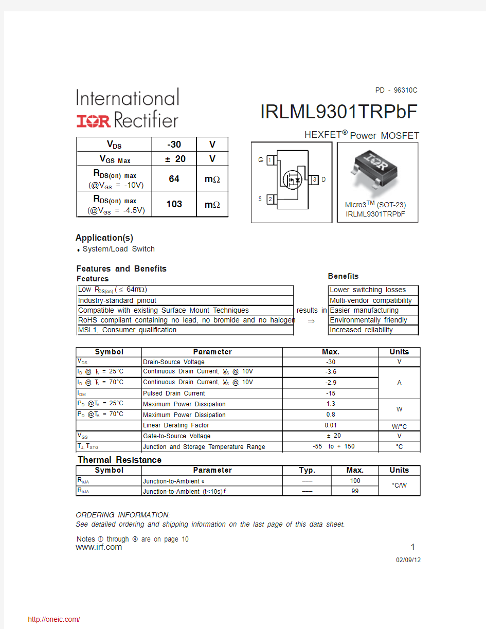
Features and Benefits
Benefits
Application(s)
? System/Load Switch
results in ?
IRLML9301TRPbF
https://www.360docs.net/doc/222856921.html,
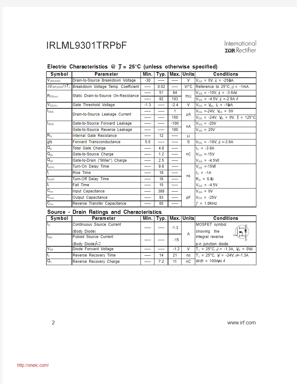
Electric Characteristics @ T = 25°C (unless otherwise specified)
IRLML9301TRPbF
3
Fig 2. Typical Output Characteristics
Fig 1. Typical Output Characteristics
Fig 4. Normalized On-Resistance
Vs. Temperature
T J , Junction Temperature (°C)
R D S (o n ) , D r a i n -t o -S o u r c e O n R e s i s t a n c e
IRLML9301TRPbF
https://www.360docs.net/doc/222856921.html,
Fig 6. Typical Gate Charge Vs.
Gate-to-Source Voltage
Fig 5. Typical Capacitance Vs.
Drain-to-Source Voltage Fig 8. Maximum Safe Operating Area
Fig 7. Typical Source-Drain Diode
Forward Voltage
1
10
100
-V DS , Drain-to-Source Voltage (V)
10
100
1000
10000
C , C a p a c i t a n c e (p F )
024681012
Q G , Total Gate Charge (nC)
2468101214
-V G S ,
G a t e -t o -S o u r c e V o l t a g e (V )
0.1
1
10
100-I S D , R e v e r s e D r a i n C u r r e n t (A )
IRLML9301TRPbF
https://www.360docs.net/doc/222856921.html, 5
Fig 11. Typical Effective Transient Thermal Impedance, Junction-to-Ambient
Fig 9. Maximum Drain Current Vs.
Ambient Temperature
Fig 10b. Switching Time Waveforms
t 1
, Rectangular Pulse Duration (sec)
25
50
75
100
125
150
T A , Ambient Temperature (°C)
00.61.21.82.433.64.2-I D , D r a i n C u r r e n t (A )
R D
V DD
V DS
V t t t t Fig 10a. Switching Time Test Circuit
IRLML9301TRPbF
https://www.360docs.net/doc/222856921.html,
Fig 13. Typical On-Resistance Vs. Drain
Current
Fig 12. Typical On-Resistance Vs. Gate
Voltage
Fig 14b. Gate Charge Test Circuit
Fig 14a. Gate Charge Waveform
5
10
15
20
25
30
35
-I D , Drain Current (A)
0100
200300
400
500
R D S (o n ), D r a i n -t o -S o u r c e O n R e s i s t a n c e (m Ω)
2
4
6
8
10
12
14
16
18
20
-V GS, Gate -to -Source Voltage (V)
20
60
100
140
180R D S (o n ), D r a i n -t o -S o u r c e O n R e s i s t a n c e (m Ω)
Id
Qgs1
Qgs2Qgd Qgodr
https://www.360docs.net/doc/222856921.html, 7
Fig 15. Typical Threshold Voltage Vs.
Junction Temperature
Fig 16. Typical Power Vs. Time
Time (sec)
P o w e r (W )
T J , Temperature ( °C )
-V G S (t h ), G a t e t h r e s h o l d V o l t a g e (V )
IRLML9301TRPbF
https://www.360docs.net/doc/222856921.html,
Micro3 (SOT-23/TO-236AB) Part Marking Information
Micro3 (SOT-23) Package Outline
Dimensions are shown in millimeters (inches)
Note: For the most current drawing please refer to IR website at: https://www.360docs.net/doc/222856921.html,/package/
1. DIMENSIONING & TOLERANCING PER ANSI Y14.5M-1994
2. DIMEN SION S ARE SHOWN IN MILLIMETERS [INCHES].
3. CONTROLLING D IMENSION: MILLIMETER.
4. DATUM PLAN E H IS LOCATED AT THE MOLD PARTING LIN E.
5. DATUM A AND B TO BE DETERMIN ED AT DATUM PLANE H.
6. D IMENSIO NS D AND E1 ARE MEASUR ED AT DATUM PLANE H. DIMENSION S D OES NO T INCLUDE MOLD PR OTRUSIO NS O R IN TER LEAD FLASH. MOLD PROTRUSIO NS O R INTERLEAD FLASH SHALL NOT EXCEED 0.25 MM [0.010 INCH] PER SIDE.
7. DIMENSION L IS THE LEAD LENGTH FOR SOLDERING TO A SUBSTRATE.
8. OUTLINE CON FO RMS TO JEDEC O UTLINE TO-236 AB.
0.89 1.12SYMBOL
MAX
MIN
A1b 0.010.10c 0.300.50D 0.080.20E 2.80 3.04E1 2.10 2.64e 1.20 1.40A 0.95BSC L 0.400.6008MILLIMETERS A20.88 1.02e1 1.90BSC REF 0.54L1BSC 0.25L2
BSC ! REF 7T8? &$ # "$INCHES 8
0 !# %7T8 "& $$ #& # '" ! ' " ! ! #0.0004MIN
MAX
## "$DIMENSIONS
Recommended Footprint
c
Note s: This pa rt ma rking inform a tion a pplie s to devic es produc e d a fter 02/26/2001
WW = (27-52) IF PREC EDED BY A LETTER
YEA R Y Z
52W W ORK W EEK 26Z
DATE CODE MARKING INSTRUCTIONS
W W = (1-26) IF PREC EDED BY LA S T DIG IT O F C ALENDAR YEA R
W ORK
F = IRLML6401O DE
LEA D FREE
DATE C O E = IRLML6402X = PART NUMBER C O DE REFERENC E:
D = IRLML5103C = IRLML6302B = IRLML2803A = IRLML2402H = IRLML5203G = IRLML2502Note : A line a bove the w ork w eek
(a s show n here ) ind ic a tes Lea d - Free .
I = IRLML0030J = IRLM L2030L = IRLM L0060M = IRLM L0040K = IRLML0100N = IRLML2060P = IRLML9301R = IRLML9303
C u W HALOG X = IRLML2244W = IRFM L8244V = IRLML6346U = IRLM L6344T = IRLML6246S = IRLM L6244Z = IRFML9244
Y = IRLM L2246
IRLML9301TRPbF
https://www.360docs.net/doc/222856921.html, 9
Micro3? (SOT-23)Tape & Reel Information
Dimensions are shown in millimeters
(inches)
2.05 ( .080 )1.95 ( .077 )
TR
FEED DIRECTION
4.1 ( .161 )3.9 ( .154 )
1.6 ( .062 )1.5 ( .060 )
1.85 ( .072 )1.65 ( .065 )
3.55 ( .139 )3.45 ( .136 )
1.1 ( .043 )0.9 ( .036 )4.1 ( .161 )3.9 ( .154 )
0.35 ( .013 )0.25 ( .010 )
8.3 ( .326 )7.9 ( .312 )
1.32 ( .051 )1.12 ( .045 )
9.90 ( .390 )8.40 ( .331 )
178.00( 7.008 ) MAX.
NOTES:
1. CONTROLLING DIMENSION : MILLIMETER.
2. OUTLINE CONFORMS TO EIA-481 & EIA-541.
Note: For the most current drawing please refer to IR website at: https://www.360docs.net/doc/222856921.html,/package/
IRLML9301TRPbF
https://www.360docs.net/doc/222856921.html,
Data and specifications subject to change without notice.
IR WORLD HEADQUARTERS: 101N.Sepulveda blvd, El Segundo, California 90245, USA Tel: (310) 252-7105
TAC Fax: (310) 252-7903
Visit us at https://www.360docs.net/doc/222856921.html, for sales contact information .02/2012
Qualification standards can be found at International Rectifier’s web site
https://www.360docs.net/doc/222856921.html,/product-info/reliability
Higher qualification ratings may be available should the user have such requirements. Please contact your International Rectifier sales representative for further information: https://www.360docs.net/doc/222856921.html,/whoto-call/salesrep/
Applicable version of JEDEC standard at the time of product release.
Notes:
Repetitive rating; pulse width limited by max. junction temperature. Pulse width ≤ 400μs; duty cycle ≤ 2%. Surface mounted on 1 in square Cu board Refer to application note #AN-994.
分销商库存信息: IR
IRLML9301TRPBF