AUO KD101N2-40NA-A1国显10.1寸TFT规格书
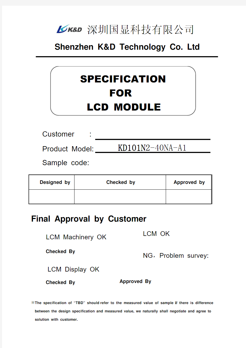
深圳国显科技有限公司
Shenzhen K&D Technology Co. Ltd
SPECIFICATION
FOR
LCD MODULE
Customer :
Product Model: KD KD KD101N 101N 101N22-40N A -A 1 Designed by
Checked by
Approved by
※The specification of “TBD” should refer to the measured value of sample . If there is difference between the design specification and measured value, we naturally shall negotiate and agree to solution with customer.
Sample code:
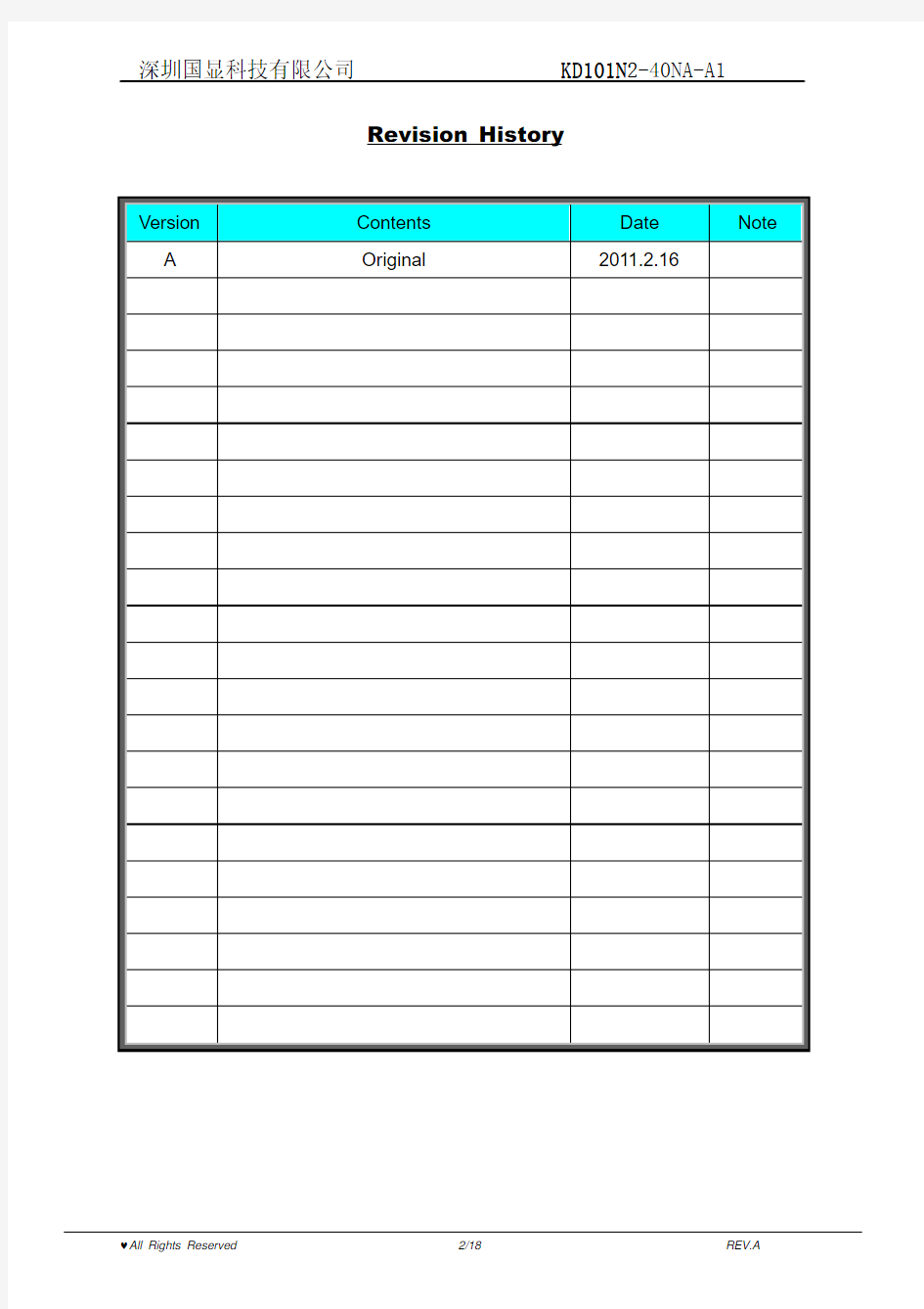
Revision History
Version Contents Date Note
A Original 2011.2.16
Contents
No. Item Page
1. Numbering System 4/18
2 Scope 5/18
3 Normative Reference 5/18
4 Definitions5/18
5 Block Diagram7/18
6 Technology Specifications7/18
7 Reliability Test Condition and Methods 15/18
8 Handling Precautions15/18
9 Precaution for use17/18
10 Package Drawing17/18 11Outline Dimension 18/18
1. Numbering System
— —
(1) (2) (3) (4) (5) (6) (7) (8)
2. Scope
This specification applies to the TFT LCD module which is designed and manufactured by LCM Factory of Shenzhen K&D Technology Co. Ltd.
3. Normative Reference
GB/T4619-1996 《Liquid Crystal Display Test Method》
GB/T2424 《Basic environmental Testing Procedures for Electric and Electronic Products.》
GB/T2423 《Basic Testing Procedures for Electric and Electronic Products》IEC61747-1 《SIXTH PARTGB2828`2829-87《National Standard of PRC》4. Definitions
4.1 Definitions of Vop
The definitions of threshold voltage Vth1, Vth2 the following typical waveforms are applied on liquid crystal by the method of equalized voltage for each duty and bias.
【selected waveform 】【non-selected waveform 】
①Vth1: The voltage which the brightness of segment indicates 50% of saturated value on the conditions of selected waveform
(f f=80Hz, Φ=10°θ=270°at 25℃)
②Vth2: The voltage which the brightness of segment indicates 50% of saturated value on the conditions of non-selected waveform
(f f=80Hz, Φ=10°θ=270°at 25℃)
③Vop: (Vth1(50%)+Vth2(50%))/2 (f f=80Hz, Φ=10°θ=270°at 25℃)
4.2 Definition of Response Time Tr, Td
①
Tr: The time required which the brightness of segment
becomes 10% from 100% when waveform is switched to
selected one from non-selected one. (f f=80Hz,
℃
Φ=10°θ=270°at 25)
②segment
Td: The time required which the brightness of
becomes 90% from 10% when waveform is switched to
selected one from selected one. (f f=80Hz, Φ=10°θ=270°at
℃
25)
4.3 Definition of Contrast Ratio Cr
Cr=A/B
① A: Segments brightness in case of non-selected waveform ② B: Segments brightness in case of selected waveform
4.4 Definition of Angle and Viewing Range
Angular Graph: Constrast Ratio
Such as:
Viewing Angle Range:
80(Cr>2) Horizontal 70(Cr>2) Vertical
5. Block Diagram
6. Technology Specifications
6.1 Features
This single-display module is suitable for use in Net Book products.
The LCD adopts one backlight with High brightness 24-lamps white LED. Construction: 10.1〞а-Si color TFT-LCD ,White LED backlight, FPC and T-CON.
6.3 Interface Pin Connection
Connector CN1 is used for electronics interface. The recommended model is IPEX-20455-040E-12 manufactured by IPEX.
Pin No. Symbol Function
1 NC No Connection(Reserve)
2 VDD Power Supply,3.3V(typical)
3 VDD Power Supply,3.3V(typical)
4 V_EDID EDID 3.3V power
5 NC No Connection(Reserve)
6 CLK_EDID EDID Clock
7 DATA_EDID EDID Data
8 Rin0- - LVDS differential data input(R0-R5,G0)
9 Rin0+ + LVDS differential data input(R0-R5,G0)
10 GND Ground
11 Rin1- - LVDS differential data input(G1-G5,B0-B1)
12 Rin1+ +LVDS differential data input(G1-G5,B0-B1)
13 GND Ground
14 Rin2- - LVDS differential data input(B2-B5,HS,VS,DE)
15 Rin2+ +LVDS differential data input(B2-B5,HS,VS,DE)
16 GND Ground
17 ClkIN- -LVDS differential clock input
18 ClkIN+ +LVDS differential clock input
19 GND Ground
20 NC No Connection(Reserve)
21 NC No Connection(Reserve)
22 GND Ground
23 NC No Connection(Reserve)
24 NC No Connection(Reserve)
25 GND Ground
26 NC No Connection(Reserve)
27 NC No Connection(Reserve)
28 GND Ground
29 NC No Connection(Reserve)
30 NC No Connection(Reserve)
31 GND Ground
32 GND Ground
33 GND Ground
34 NC No Connection(Reserve)
35 PWM LED BLU Brightness Control(Note 1,2)
36 LED-EN/NC LED Converter Enable(3.3V)/NC
37 NC No Connection(Reserve)
38 VLED LED Converter Input Power(5V~21V)
39 VLED LED Converter Input Power(5V~21V)
40 VLED LED Converter Input Power(5V~21V)
Note1: PWM is used to adjust the B/Lbrightness.
Note 2: PWM signal=0~3.3V, Operation Frequency:100 Hz~20KHz,
6.4 Absolute Max. Rating
Values
Item Symbol
Unit
Min. Max.
V CC -0.3 4.0 V Power Voltage
V LED-0.3 5.5 V Input Signal Voltage V I -0.3 V CC V Operation Temperature T OP -20 70 ℃Storage Temperature T ST -30 80 ℃6.5 Typical Operation Conditions
Values
Unit Item Symbol
Min. Typ. Max.
V CC 3.0 3.3 3.6 V Power Voltage
V LED - 9.5 - V
I CC- TBD - mA
Current Consumption
I LED- 180 - mA
6.6 Power Sequence
Power Supply Vcc
Data Signal
ADJ
t 4 50mSec ≧
Note: Data Signal includes Rin0- ~ Rin2-,Rin0+ ~ Rin2+,CLKIN- , CLKIN+.
6.7 Timing Conditions
Switching Characteristics
Values Item
Symbol Min. Typ. Max. Unit Remark RxCLKIN Period t RCP 11.76 T 50 ns Note 1 RxCLKIN High Time t RCH - T/2 - ns RxCLKIN Low Time
t RCL - T/2 - ns PAD0/1 to RxCLKIN Delay t RCD - 3T/7 - ns Data Setup to RxCLKIN t RS 1.9 - - ns Data Hold from RxCLKIN
t RH 3.0 - - ns
Input Data Position 0(T=11.76ns) T RIP1 -0.4 0 0.4 ns Note 2 Input Data Position 1(T=11.76ns) T RIP0 T/7-0.4 T/7 T/7+0.4 ns Note 2 Input Data Position 2(T=11.76ns) T RIP6 2T/7-0.4 2T/7 2T/7+0.4 ns Note 2 Input Data Position 3(T=11.76ns) T RIP5 3T/7-0.4 3T/7 3T/7+0.4 ns Note 2 Input Data Position 4(T=11.76ns) T RIP4 4T/7-0.4 4T/7 4T/7+0.4 ns Note 2 Input Data Position 5(T=11.76ns) T RIP3 5T/7-0.4 5T/7 5T/7+0.4 ns Note 2 Input Data Position 6(T=11.76ns) T RIP2
6T/7-0.4
6T/7
6T/7+0.4
ns
Note 2
Input Timming(only for DE Mode)
Parameter Min Typ Max Unit H-Total 1185 1344 1800 CLK H-Active 1024 1024 1024 CLK H-Blanking 161 320 776 CLK V-Total 628 635 650 LINE V-Active 600 600 600 LINE V-Blanking 28 35 50
LINE
Timing Diagram
6.8 Optical specifications Values Item
Symbol
Condition
Min. Typ. Max. Unit
Remark
θL Φ=180°(9 o’clock) - 60 - θR Φ=0°(3 o’clock) - 60 - θT Φ=90°(12 o’clock) - 30 - Viewing angle (CR ≥ 10) θB Φ=270°(6 o’clock)
- 50 - degree
Note 1
Response time Rise+Fall T RT - 16 25 msec Note 3 Contrast ratio CR 400 500 - -
Note 4 W X 0.28 0.31 0.35 - Color chromaticity
W Y 0.29 0.33 0.36 - Note 2 Note 5 Note 6 Luminance L - 200 - Cd/m2- Note 6 Luminance uniformity
Y U
Normal θ=Φ=0°
70
75
-
%
Note 6,7
Note 1: Definition of viewing angle range
Fig. 4-1 Definition of viewing angle
Note 2: Definition of optical measurement system.
The optical characteristics should be measured in dark room. After 30 minutes operation, the optical properties are measured at the center point of the LCD screen. (Viewing angle is measured by ELDIM-EZ contrast/Height :1.2mm ,Response time is measured by Photo detector TOPCON BM-7, other items are measured by BM-5A/Field of view: 1° /Height: 500mm.)
Normal line
θ=Φ=0° Φ=270°
6 o’clock direction
Φ=0°
ΦΦ=0°
Φ=180°
Normal line
Fig. 4-2 Optical measurement system setup
Note 3: Definition of Response time
The response time is defined as the LCD optical switching time interval between “White” state and “Black” state. Rise time (T ON ) is the time between photo detector output intensity changed from 90% to 10%. And fall time (T OFF ) is the time between photo detector output intensity changed from 10% to 90%.
Fig. 4-3 Definition of response time
Note 4: Definition of contrast ratio
state Black"" the on LCD
when measured Luminance state
White"" the on LCD when measured Luminance (CR) ratio Contrast =
Note 5: Definition of color chromaticity (CIE1931)
Color coordinates measured at center point of LCD.
Note 6: All input terminals LCD panel must be ground while measuring the center
area of the panel. The LED driving condition is V LED =5.0V.
90%
10% 0%
P h o t o d e t e c t o r o u t p u t (R e l a t i v e v a l u e )
ON
White (TFT OFF)
Black (TFT ON)
White (TFT OFF)
Note 7: Definition of Luminance Uniformity
Active area is divided into 9 measuring areas (Refer to Fig. 4-4 ).Every measuring point is placed at the center of each measuring area.
max min B B (Yu)Uniformity Luminance =
L-------Active area length W----- Active area width
Fig. 4-4 Definition of measuring points
B max : The measured maximum luminance of all measurement position. B min : The measured minimum luminance of all measurement position.
7. Reliability Test Conditions And Methods
Item Test Conditions Remark High Temperature Storage Ta = 80℃96 hrs
Low Temperature Storage Ta =-30℃96hrs
High Temperature Operation Ts = 70℃96hrs
Low Temperature Operation Ta = -20℃96hrs
Operate at High Temperature and Humidity +60,
℃ 90%RH max. 96 hrs Operation
Thermal Shock -20~ +
℃70℃ 100 cycles 2Hrs/cycle Non-operation
Electrostatic Discharge Contact=±4KV, class B Air=±8KV, class B
Vibration Test Frequency range:8~33.3Hz
Stroke:1.3mm
Sweep:2.9G 33.3~400Hz
2 hours for each direction of X. Y. Z.
(6 hours for total)
Non-operation
JIS C7021,A-10
ConditionA:
15minutes
Mechanical Shock 100G 6ms,±X, ±Y, ±Z 3 times for each
direction
Non-operation
JIS C7021,A-7
ConditionC
Vibration(With Carton) Random Vibration :
0.015G*G/Hz from 5-200HZ,
-6dB/Octave from 200-500HZ
IEC68-34
Drop(With Carton) Height:60 cm
1 corner, 3 edges, 6 surfaces
Electro Static Discharge ± 2KV, Human Body Mode, 100pF/1500?
8. Handling Precautions
8.1 Mounting method
The LCD panel of Daxian LCD module consists of two thin glass plates with polarizes which easily be damaged. And since the module in so constructed as to be fixed by utilizing fitting holes in the printed circuit board.
Extreme care should be needed when handling the LCD modules.
8.2 Caution of LCD handling and cleaning
When cleaning the display surface, Use soft cloth with solvent
[recommended below] and wipe lightly
Isopropyl alcohol
Ethyl alcohol
Do not wipe the display surface with dry or hard materials that will damage the polarizer surface.
Do not use the following solvent:
Water
Aromatics
Do not wipe ITO pad area with the dry or hard materials that will damage the ITO patterns
Do not use the following solvent on the pad or prevent it from being contaminated:
Soldering flux
Chlorine (Cl) , Salfur (S)
If goods were sent without being sili8con coated on the pad, ITO patterns could be damaged due to the corrosion as time goes on.
If ITO corrosion happen by miss-handling or using some materials such as Chlorine (CI), Salfur (S) from customer, Responsibility is on customer.
8.3 Caution against static charge
The LCD module use C-MOS LSI drivers, so we recommended that you: Connect any unused input terminal to Vdd or Vss, do not input any signals before power is turned on, and ground your body, work/assembly areas, assembly equipment to protect against static electricity.
8.4 packing
Module employ LCD elements and must be treated as such.
Avoid intense shock and falls from a height.
To prevent modules from degradation, do not operate or store them exposed direct to sunshine or high temperature/humidity
8.5 Caution for operation
It is an indispensable condition to drive LCD’s within the specified voltage limit since the higher voltage then the limit cause the shorter LCD life.
An electrochemical reaction due to direct current causes LCD’s undesirable deterioration, so that the use of direct current drive should be avoided.
Response time will be extremely delayed at lower temperature then the operating temperature range and on the other hand at higher temperature LCD’s how dark color in them. However those phenomena do not mean malfunction or out of order with LCD’s, which will come back in the specified operation temperature.
If the display area is pushed hard during operation, some font will be abnormally displayed but it resumes normal condition after turning off once.
A slight dew depositing on terminals is a cause for electro-chemical reaction
resulting in terminal open circuit.
Usage under the maximum operating temperature, 50%Rh or less is required.
8.6 storage
In the case of storing for a long period of time for instance, for years for the purpose or replacement use, the following ways are recommended.
Storage in a polyethylene bag with the opening sealed so as not to enter fresh air outside in it . And with no desiccant.
Placing in a dark place where neither exposure to direct sunlight nor light’s keeping the storage temperature range.
Storing with no touch on polarizer surface by the anything else.
[It is recommended to store them as they have been contained in the inner container at the time of delivery from us
8.7 Safety
It is recommendable to crash damaged or unnecessary LCD’s into pieces and
wash off liquid crystal by either of solvents such as acetone and ethanol, which should be burned up later.
When any liquid leaked out of a damaged glass cell comes in contact with your hands, please wash it off well with soap and water
9. Precaution for use
9.1
A limit sample should be provided by the both parties on an occasion when the both parties agreed its necessity. Judgment by a limit sample shall take effect after the limit sample has been established and confirmed by the both parties.
9.2
On the following occasions, the handing of problem should be decided through discussion and agreement between responsible of the both parties.
When a question is arisen in this specification
When a new problem is arisen which is not specified in this specifications When an inspection specifications change or operating condition change in customer is reported to Daxian , and some problem is arisen in this specification due to the change
When a new problem is arisen at the customer’s operating set for sample evaluation in the customer site.
10. Package Drawing
11. Outline Dimension
TDK贴片电容型号选型规格书
C1005X5R1A475KTJ00E0402 X5R 10V 4.5UF 10% C1005X5R1E224KT000E0402 X5R 25V 220NF 10% C1005X5R1E225KT000E0402 X5R 25V 2.2UF 10% C1005X7R1C104KT000F0402 X7R 16V 100NF 10% C1005X7R1C224kT000E0402 X7R 16V 220NF 10% C1005X7R1H104KT000F0402 X7R 50V 100NF 10% C1608C0G1E103JT000N0603 C0G 25V 10NF 5% C1608C0G1H101JT000N0603 C0G 50V 100PF 5% C1608C0G1H152JT000N0603 C0G 50V 1.5NF 5% C1608C0G1H221JT000N0603 C0G 50V 220PF 5% C1608C0G1H222JT000N 0603 C0G 50V 2.2NF 5% C1608C0G1H472JT000N0603 C0G 50V 4.7NF 5% C1608C0G1H562JT000N0603 C0G 50V 5.2NF 5% C1608X5R0J106MTJ00N0603 X5R 6.3V 10UF 20% C1608X5R0J225KT000N0603 X5R 6.3V 2.2UF 10% C1608X5R0J226MT000N0603 X5R 6.3V 22UF 20% C1608X5R0J335KT000N0603 X5R 6.3V 3.3UF 10% C1608X5R0J475KT000N0603 X5R 6.3V 4.7UF 10% C1608X5R1A105KTJ00N0603 X5R 10V 1UF 10% C1608X5R1A106MT000E0603 X5R 10V 10UF 20% C1608X5R1A225KT000E0603 X5R 10V 2.2UF 10% C1608X5R1A226MTE00E0603 X5R 10V 22UF 20% C1608X5R1A475KT000N0603 X5R 10V 4.7UF 10% C1608X5R1C225KT000N0603 X5R 16V 2.2UF 10%
贴片电阻规格 封装 尺寸
贴片电阻规格、封装、尺寸 ChipR Dimensions 、Footprint 简述 基本结构 分类 规格、封装、 尺寸 额定功率及工 作电压 阻值,标准阻 值 标识 规格书、生产 厂家
命名方法 价格、报价 创建时间:2005-12-30 最后修改时间:2006-10-29 贴片电阻套件 为方便学生、研发人员试验和产 品试制,特推出片式电阻系列套 件。 我们常说的贴片电阻 (SMD Resistor)叫"片式固定电阻器"(Chip Fixed Resistor),又叫"矩形片状电阻"(Rectangular Chip Resistors),是由ROHM 公司发明并最早推出市场的。特点是耐潮湿,耐高温,可靠度高,外观尺寸均匀,精确且温度系数与阻值公差小。 按生产工艺分厚膜(Thick Film Chip Resistors)、薄膜(Thin Film Chip Resistors )两种。厚膜是采用丝网印刷将电阻性材料淀积在绝缘基体(例如玻璃或氧化铝陶瓷)上,然后烧结形成的。我们通常所见的多为厚膜片式电阻,精度范围±0.5% ~ 10%,温度系数:±50PPM/℃~ ±400PPM/℃。薄膜是在真空中采用蒸发和溅射等工艺将电阻性材料淀积在绝缘基体工艺(真空镀膜技术)制
成,特点是低温度系数(±5PPM/℃),高精度(±0.01%~±1%)。 封装有:0201,0402,0603,0805,1206,1210,1812,2010,2512。其常规系列的精度为5%,1%。阻值范围从0.1欧姆到20M欧姆。标准阻值有E24,E96系列。功率有1/20W、1/16W、1/8W、1/10W、1/4W、1/2W、1W。 特性: 体积小,重量轻 适合波峰焊和回流焊 机械强度高,高频特性优越 常用规格价格比传统的引线电阻还便宜 生产成本低,配合自动贴片机,适合现代电子产品规模化生产使用状况:由于价格便宜,生产方便,能大面积减少PCB面积,减少产品外观尺寸,现在已取代绝大部分传统引线电阻。除一些小厂或不得不使用引线电阻的设计,各种电器上几乎都在使用。目前绝大部分电子产品,以0603、0805器件为主;以手机,PDA为代表的高密度电子产品多使用0201、0402的器件;一些要求稳定和安全的电子产品,如医疗器械、汽车行驶记录仪、税控机则多采用1206、1210等尺寸偏大的电阻。 市场状况:目前,在全球的市场份额中,排名依次是台湾、日本、中国、韩国,欧美几乎不再生产。主要的生产厂商几乎都在中国建立生产基地。台湾国巨(Yageo)公司为世界上第一大生产商。日本企业则生产一些如0201、0402、高精度、高电压,具有工艺难度,利润高的系列。台湾及国内工厂则多生产些
友达5.7寸液晶屏G057VTN01 V0规格书-杭州旭虹科技有限公司
G057VTN01 V0 Color TFT-LCD Module 5.7” VGA Landscape LED Backlight Wide Temperature Range Mercury-free solution RoHS and Halogen-free Compliance High Shock/Vibration Resistance Outline and Interface are fully compatible with G057VN01 serials (Preliminary) Size (inch) 5.7” Model G057VN01 V210 Resolution (pixel) 640(RGB) x 480 Active Area (mm) 115.2(H) x 86.4(V) Pixel Pitch (mm) 0.18 x 0.18 Mode TN LCD Surface Anti-Glare, Hardness 3H Number of Colors 262K View Angle (L/R/U/D) 80/80/70/70 (typ.) Brightness(nit) (25℃) 500(min.), 600 (typ.) Contrast Ratio (25℃) 800:1 (typ.) Response Time (ms) 25 (typ.) LED Life (hrs.) 50K Power Consumption (W) 3.74W Supply Voltage (V) 3.3V Storage Temp. (℃) -30 ~ 85 Operation Temp. (℃) -30 ~ 85 Outline Dimension (mm) 144.0(H) x 104.6(V) x 12.3(D) (typ.) Weight (g) 150g (typ.), 165g (max.) Interface CMOS
通用型贴片电容规格书(选型手册)
【 南京南山半导体有限公司 — 贴片电容选型资料】
https://www.360docs.net/doc/293117830.html,
MULTILAYER CHIP CERAMIC CAPACITOR
COG/COH
COG
, ,
-55
125
,
0
30ppm/
0
60ppm/
0805
CG
101
J
500
N
T
(PF) ( 0402 0.04 0603 0.06 0805 0.08 1206 0.12 ) 0.02 0.03 0.05 0.06 1.00 1.60 2.00 3.20 ( ) 0.50 0.80 1.25 1.60 CG CH COG NPO COH 100 101 102 10 10
0 1
J G C B D
5.00% 2.00% 0.25PF 0.10PF 0.50PF
10 10 10 10
2
6R3 100 250 500
6.3V 10V 25V 50V
S C N / / T B
WB
W
T
L mm L 0402 0603 0805 1206 1005 1608 2012 3216 1.00 1.60 2.00 3.20 0.05 0.10 0.20 0.30 W 0.50 0.80 1.25 1.60 0.05 0.50 0.10 0.80 0.20 0.80 1.00 1.25 0.20 0.80 1.00 1.25 T WB 0.05 0.25 0.10 0.30 0.20 0.50 0.20 0.20 0.20 0.60 0.20 0.20 0.10 0.10 0.20 0.30
15
OLED2.4寸显示屏 液晶屏 规格书
、结构尺寸Structure Size 一5V 供电5V IO 电平二、接口定义Pin Assignment(P2&P3)序号(No.) 定义(SYMBOL )说明(Description )1 VCC3.3数字电路电源电压Power Supply for Logic Circuit 2 VCC3.3数字电路电源电压Power Supply for Logic Circuit 3 EN 模块13v OLED 供电使能信号,高有效OLE Panel Power Enable Signal active High to Enable ,默认内部弱上拉,可不接。4 GND 数字电路电源地Ground of Logic Circuit 5 CS 片选信号Chip Select 低有效,6 RES 复位信号Power Reset 低有效,需IO 引脚控制7 D/C 数据与命令控制信号Data/Command Control 高为数据,低为命令。需IO 引脚控制8 GND 数字电路电源地Ground of Logic Circuit 9 SCLK SPI 时钟信号Serial Clock of SPI 。需IO 引脚控制10SDIN SPI 输入信号Serial Data of SPI 。需IO 引脚控制 OLED2.4寸1309_3.3V
一、产品介绍General Specifications Diagonal Size尺寸 2.4” Color颜色Yellow、Green、Blue、White Type类型Monochrome Pixel Number分辨率128x64 Module Size(mm)模组尺寸62.1×53.3×9 Active Size(mm)显示区域55.01×27.49 Driver IC驱动IC SSD1309 Interface接口4_Wire SPI Supply Voltage供电电压 3.3V Voltage Range建议电压范围 1.65V~3.3V Max Voltage最大极限电压4V Min Voltage最小极限电压 1.65V View Angle视角>160degree全视角 Contrast对比度>10000:1 Brightness(cd/m2)亮度(绿色)120(Typ)@13V(20000Hours) Power功耗由点亮的像素决定 30%像素点亮<260mw 50%像素点亮<345mw 100%像素点亮(实际使用中用不到)<515mw Brightness(cd/m2)(黄色)80(Typ)@13V(15000Hours) Power功耗由点亮的像素决定 30%像素点亮<260mw 50%像素点亮<380mw 100%像素点亮(实际使用中用不到)<590mw Brightness(cd/m2)(白色)80(Typ)@13V(30000Hours) Power功耗由点亮的像素决定 30%像素点亮<300mw 50%像素点亮<440mw 100%像素点亮(实际使用中用不到)<690mw Brightness(cd/m2)(蓝色)80(Typ)@13V(15000Hours) Power功耗由点亮的像素决定 30%像素点亮<325mw 50%像素点亮<470mw 100%像素点亮(实际使用中用不到)<720mw Weight(g)重量8.6 Assembly连接方式10Pin1.0mm FPC Connector and2.54mm Metal pins
国巨电容规格
电容命名规则及采购信息要求 (一)国巨贴片电容的命名: 贴片电容的命名所包含的参数有贴片电容的尺寸、容值精度、贴片电容的材质、电压、电容容量、端头材料以及包装要求。 例国巨贴片电容CC0805JRNPO9BN101 CC:表示国巨电容系列名称——多层陶瓷贴片电容。国巨电容的系列 还有CA(表示排容),CH(表示高频电容)等等。 0805:表示尺寸,长度为0.08英寸,宽度为0.05英寸。此外,常见 的电容尺寸还有0201,0402,0603,1206,1210,1808,1812等。 J:表示电容容量的误差精度为±5%;另外B=±0.1PF,C=±0.25PF,D= ±0.5PF,F=±1PF,G=±2PF,K=±10%,M=±20%,Z=-20%~+80%。 R:表示7寸盘纸带包装。 NPO:表示电容材质。此外,常用的电容材质还有X5R,X7R,Y5V。 9:表示电压为50V。4=4V, 5=6.3V, 6=10V, 7=16V, 8=25V, 0=100V, A=200V, B=500V, C=1KV, D=2KV, E=3KV等(注意:100V是用数字0 表示,不是字母O) B:表示端头材料是镍电极。 N:表示NPO。 101:表示容值,前面两个数字为有效数字,第三个数字表示有几个 零。101=100PF, 102=1000PF, 103=10,000PF……以此类推。
(二)贴片电容的尺寸表示方法 贴片电容的尺寸表示法有两种,一种是以英寸为单位来表示,一种是以毫米为单位来表示。以英寸为单位来表示的称为英制尺寸,以毫米为单位来表示的称为公制尺寸。国巨贴片电容通常用英制尺寸来表示。
诺瓦科技LED显示屏控制台C1规格书
C1 Desktop Console Specifications Xi’an NovaStar Tech Co., Ltd.
Copyright ?2018 Xi’an NovaStar Tech Co., Ltd. All Rights Reserved. No part of this document may be copied, reproduced, extracted or transmitted in any form or by any means without the prior written consent of Xi’an NovaStar Tech Co., Ltd. Trademark is a trademark of Xi’an NovaStar Tech Co., Ltd. Statement You are welcome to use the p roduct of Xi’a n NovaStar Tech Co., Ltd. (hereinafter referred to as NovaStar). This document is intended to help you understand and use the product. For accuracy and reliability, NovaStar may make improvements and/or changes to this document at any time and without notice. Any problem in use or any good suggestion, please contact us through ways provided in the document. We will do our utmost to solve the problems and adopt the suggestions after evaluation as soon as possible. Website:http://w ww.novastar.te c h
(完整版)贴片电容的介绍
X7R 性质: 1. 介电常数可达到3000,容温变化率小于15%,介电损耗小于3.5%; 2. 粉体粒径250-300nm,烧成陶瓷晶粒尺寸300-400nm。 电镜照片: 用途: 1. 此介质材料为环保型粉料,无任何有毒镉(Cd)和铅(Pd)的化合物; 2. 适合于制备超薄层大容量贱金属内电极多层陶瓷电容器的生产:单层陶瓷膜片厚度5~10mm;层数从几十到几百层;电容量从 0.1 nF 到100 nF; 3. 由于瓷粉粒度小,分散性好,因此不需要再进行剧烈的球磨,以免改变瓷料的晶粒性质,使性能劣化。 Y5V贴片电容,MLCC Y5V多层陶瓷片式电容 贴片电容简述 COG(NPO)贴片电容选型表 X7R贴片电容选型表 创建时间:2006-1-13 最后修改时间:2006-1-13 简述 Y5V贴片电容属于EIA规定的Class 2类材料的电容。它的电容量受温度、电压、时间变化影响大。
Y5V贴片电容特性 ?具有较差的电容量稳定性,在-25℃~85℃工作温度范围内,温度特性为+30%,-80%。 ?层叠独石结构,具有高可靠性。 ?优良的焊接性和和耐焊性,适用于回流炉和波峰焊。 ?应用于温度变化小的退耦、隔直等电路中。 Y5V贴片电容各个生产厂家规格书 生产厂家规格书 AVX Datasheet 风华Datasheet 国巨Datasheet 太阳诱电Datasheet 村田Datasheet Y5V贴片电容容量范围 厚度与符号对应表 符 号 A C E G J K M N P Q X Y Z 最 大 厚 度毫米(英寸) 0.33 (0.013 ) 0.56 (0.022 ) 0.71 (0.028 ) 0.86 (0.034 ) 0.94 (0.037 ) 1.02 (0.040 ) 1.27 (0.050 ) 1.40 (0.055 ) 1.52 (0.060 ) 1.78 (0.070 ) 2.29 (0.090 ) 2.54 (0.100 ) 2.79 (0.110 ) 0201~1210 Y5V贴片电容选型表 封装尺寸0201 0402 0603 0805 1206 1210 工作电压6. 3 1 6. 3 1 1 6 2 5 5 6. 3 1 1 6 2 5 5 6. 3 1 1 6 2 5 5 6. 3 1 1 6 2 5 5 6. 3 1 1 6 2 5 5 电容量(pF ) 820 1000 2200 4700 A A A C 电容量(uF 0.01 0.02 2 A A A A C C C C C G G G G
P6户外全彩LED显示屏规格书
P6户外表贴全彩LED显示屏规格书 绿色大地P6户外表贴全彩LED显示屏显著特点: ■采用高端优质芯片,屏体亮度达6500CD每平方以上绿色大地照明科技充分满足户外亮度要求;亮度100级可调。 ■采用高端电源供应商电源,100-230V宽电压输入,切实保证屏体供电稳定。 ■与IC行业巨头台湾聚积携手,装配高精度驱动芯片,显示画面展现完美的色彩一致性。■采用行业领先控制系统,真正实现逐点校正功能。 ■箱体融入最先进设计理念,结构轻巧,安装便捷,样式美观。 ■全新面罩设计,大大提升屏体对比度及平整度,同时新款面罩具有强劲的抗干扰与抗老化功能。 ■PCB板精选板材,1.5 OZ铜厚,加上独特的PCB板设计工艺,使显示屏稳定性更高、节能性更强、功耗更低。
P6户外表贴屏箱体(480*480MM)4*2个箱体效果图
P6户外表贴显示屏还有如下特点 1)、系统设计先进合理,显示效果清晰稳定,安装维护方便。 2)、全天候工作:色彩逼真、刷新频率高、防静电、散热效果好、性价比高。 3)、显示方式:左右移动、上下移动、左拉幕、右拉幕、中开合、闪烁、即显等多种方式。 4)、使用节目编辑播放软件,可通过、鼠标编辑、增加、删除和修改文字、图形、图像等信息。编排的内容存于控制卡, 信息播放按节目表自动循环显示。 5)、发光亮度强:发光强度强,并且亮度可调。 6)、视角度好:在水平和垂直均有较大的可视角度,这对水平分布广和高度落差较大的环境均适合。 7)、效果好:采用非线性逐点校正技术,文字更清晰、层次感更强; 8)、可靠性强:采用分布式扫描技术和模块化设计技术,可靠性、稳定性更高; 9)、显示模式多样化:支持多种显示模式; 10)、操作方便:电脑编辑内容发送到系统控制卡,就可显示编辑的内容,系统操作十分方便。 11)、适用范围:商场、企业、学校、舞台、银行、证券、公安、交通、工商、电力、海关、 医院、公园、机场、车站、 体育场馆等领域户外租赁显示。 P3全彩显示屏技术参数 LED 屏体波长控制在2.5nm 之内,屏体亮度≥ 6500cd/㎡
国巨电容规格书
1. SUBJECT: This specification applies on the chip capacitor made by Yageo Corporation. 2. PART NUMBER: Part number of the chip capacitor is identified by the size, tolerance, packing, material and capacitor value. Example:
3. ELECTRICAL CHARACTERISTICS
4. DIMENSION (mm) L W T L 1;L 2 L 3 Style MIN. MAX. MIN. MAX. Min. CC0402 1.0±0.05 0.5±0.05 0.45 0.55 0.15 0.30 0.40 CC0603 1.6±0.10 0.8±0.10 0.70 0.90 0.20 0.60 0.40 CC0805 2.0±0.10 1.25±0.10 0.50 1.35 0.25 0.75 0.55 CC1206 3.2±0.15 1.6±0.15 0.50 1.35 0.25 0.75 1.40 CC1210 3.2±0.20 2.5±0.20 0.50 1.80 0.25 0.75 1.40 CC1812 4.5±0.20 3.2±0.20 0.50 1.80 0.25 0.75 2.20 CC2220 5.7±0.20 5.0±0.20 0.50 1.80 0.25 0.75 2.20 Unit: mm
液晶屏ZJ070NA-01P规格书
CHIMEI INNO L U X DISPLAY CORPORATION LCD MODULE SPECIFICATION Customer: Model Name: ZJ070NA-01P Date: 2012/01/11 Version: 01 ■Preliminary Specification □Final Specification For Customer ’s Acceptance Approved by Comment Approved by Reviewed by Prepared by Charlie Chou 2012/02/01 Wenyi Wang 2012/02/01 David Lee 2012/01/31 深显实业有限公司 https://www.360docs.net/doc/293117830.html,
CHIMEI InnoLux copyright 2004 All rights reserved, Copying forbidden. Record of Revision Version Revise Date Page Content Pre-Spec.01 2012/01/11 Initial Release.
CHIMEI INNO L U X Contents 1. General Specifications (1) 2. Pin Assignment (2) 3. Operation Specifications (5) 3.1. Absolute Maximum Ratings (5) 3.1.1. Typical Operation Conditions (6) 3.1.2. Current Consumption (7) 3.1.3. Backlight Driving Conditions (7) 3.2. Power Sequence (8) 3.3. Timing Characteristics (9) 3.3.1. AC Electrical Characteristics (9) 3.3.2. Input Clock and Data Timing Diagram (9) 3.3.3. DC Electrical Characteristics (10) 3.3.4. Timing (11) 3.3.5. Data Input Format (12) 4. Optical Specifications (13) 5. Reliability Test Items (17) 6. General Precautions (18) 6.1. Safety (18) 6.2. Handling (18) 6.3. Static Electricity (18) 6.4. Storage (18) 6.5. Cleaning (18) 7. Mechanical Drawing (19) 8. Package Drawing (20) 8.1. Packaging Material Table (20) 8.2. Packaging Quantity (20) 8.3. Packaging Drawing (21)
贴片电容的精度规格书
贴片电容的精度规格书 容量与误差:实际电容量和标称电容量允许的最大偏差范围。 一般分为3级:I级±5%,II级±10%,III级±20%。 在有些情况下,还有0级,误差为±20%。精密电容器的允许误差较小,而电解电容器的误差较大,它们采用不同的误差等级。常用的电容器其精度等级和电阻器的表示方法相同。用字母表示:D——005级——±0.5%;F——01级——±1%;G——02级——±2%;J——I级——±5%;K——II级——±10%;M——III级——±20%。 一、电容的型号命名: 1) 各国电容器的型号命名很不统一,国产电容器的命名由四部分组成:第一部分:用字母表示名称,电容器为C。 第二部分:用字母表示材料。 第三部分:用数字表示分类。 第四部分:用数字表示序号。 2) 电容的标志方法: (1) 直标法:用字母和数字把型号、规格直接标在外壳上。 (2) 文字符号法:用数字、文字符号有规律的组合来表示容量。文字符号表示其电容量的单位:P、N、u、m、F等。和电阻的表示方法相同。
标称允许偏差也和电阻的表示方法相同。小于10pF的电容,其允许偏差用字母代替:B——±0.1pF,C——±0.2pF,D——±0.5pF,F——±1pF。(3) 色标法:和电阻的表示方法相同,单位一般为pF。小型电解电容器的耐压也有用色标法的,位置靠近正极引出线的根部,所表示的意义如下表所示: 颜色 黑 棕 红 橙 黄 绿 蓝 紫 灰 耐压 4V 6.3V 10V16V25V32V40V50V 63V (4) 进口电容器的标志方法:进口电容器一般有6项组成。 第一项:用字母表示类别: 第二项:用两位数字表示其外形、结构、封装方式、引线开始及与轴的关系。 第三项:温度补偿型电容器的温度特性,有用字母的,也有用颜色的,其意义如下表所示: 序号 字母 颜色 温度系 数 允许 偏差 字母 颜色 温度系数 允许 偏差 1 A 金 +100 R 黄 -220 2 B 灰 +30 S 绿 -330 3 C 黑 0 T 蓝 -470
国巨贴片电容知识
国巨贴片电容知识 一、国巨贴片电容的命名: 贴片电容的命名所包含的参数有贴片电容的尺寸、容值精度、贴片电容的材质、电压、电容容量、端头材料以及包装要求。 例如:国巨贴片电CC0805JRNPO9BN101容 CC:表示国巨电容系列名称——多层陶瓷贴片电容。国巨电容的系列还有CA(表示排容),CH(表示高频电容)等等。 0805:表示尺寸,长度为0.08英寸,宽度为0.05英寸。此外,常见的电容尺寸还有0201,0402,0603,1206,1210,1808,1812等。 J:表示电容容量的误差精度为±5%;另外B=±0.1PF,C=±0.25PF,D=±0.5PF,F=±1PF,G=±2PF,K=±10%,M=±20%,Z=-20%~+80%。 R:表示7寸盘纸带包装。 NPO:表示电容材质。此外,常用的电容材质还有X5R,X7R,Y5V。9:表示电压为50V。4=4V, 5=6.3V, 6=10V, 7=16V, 8=25V, 0=100V, A=200V, B=500V, C=1KV, D=2KV, E=3KV等(注意:100V是用数字0表示,不是字母O) B:表示端头材料是镍电极。 N:表示NPO。 101:表示容值,前面两个数字为有效数字,第三个数字表示有几个零。101=100PF, 102=1000PF, 103=10,000PF……以此类推。
二、英制尺寸与公制尺寸的对应表: TDK贴片电容的参数识别 积层贴片陶瓷片式电容器 C 2012 X7R 1H 104 K T 系列名称体积材料电压容量误差包装 0603=0201 CH 0J=6.3V C=0.25 T=卷带1005=0402 COG 1A=10V D=0.5 B=袋装1608=0603 JB 1C=16V J=5% 2012=0805 JF 1E=25V K=10% 3216=1206 X7R 1H=50V M=20% 3225=1210 X5R 2A=100V Z=+80-20% 4532=1812 Y5V 2E=250V 5650=2220 2J=630V 4520=1808 3A=1KV 3D=2KV 3F=3KV
中高压电容器MLCC贴片电容器规格书
中高压电容器HIGH VOLTAGE MLCC 中高压多层片状陶瓷电容器是在多层片状陶瓷电容器的工艺技术、设备基础上,通过采用特殊工艺制作的一种具有良好高压可靠性的产品,该产品适合于表面贴装,适合于多种直流高压线路,可以有效的改善电子线路的性能。●应用范围 ※模拟或数字调制解调器 。※局域网/广域网接口界面。※日光灯启动辉器照明电路。※倍压电器。※直流变送器。※背光源驱动电路。 Middle & high voltage MLCC is a kind of special design 、special technology MLCC that bases on the technology of general MLCC. This kind of MLCC has stable high voltage reliability and suitable to SMT. Middle & high MLCC is widely applicable for many direct high voltage circuits in which it can improve the performance of the circuit. ●APPLICATIONS ※Analog & Digital Modems ※LAN/WAN Interface ※Lighting Ballast Circuits ※V oltage Multipliers ※DC-DC Converters ※Back-lighting Inverters 容量范围及其电压 单位/unit: pF 尺寸规格容量范围Capacitance Size Code 工作电压Rated V oltage NPO X7R Y5V 100V 0.5~820 150~10,000 2,200~68,000 200V 0.5~470 150~6,800 ---------- 0603 250V 0.5~470 150~6,800 ---------- 100V 0.5~1,500 150~33,000 10,000~100,000 200V 0.1~1,500 150~22,000 10,000~56,000 250V 0.1~1,500 150~22,000 10,000~56,000 500V 0.1~560 150~10,000 --------- 0805 1000V 0.1~100 --------- --------- 100V 0.5~3,300 150~100,000 15,000~330,000 200V 0.1~2,700 150~47,000 10,000~150,000 250V 0.1~2,700 150~33,000 10,000~150,000 500V 0.1~1,500 150~22,000 ---------- 1000V 0.1~1,000 150~5,600 ---------- 1206 2000V 0.1~270 150~1,500 -----------
贴片电容电阻参数及详解
公司主营产品相关知识 一.贴片电容 贴片电容全称:多层(积层,叠层)片式陶瓷电容器,也称为贴片电容,片容。英文缩写:MLCC。 1.品牌: 日系:TDK 、村田(MURATA)、京瓷(Kyocera)、太阳诱电(TAIYO YUDEN)、松下(Panasonic)、罗姆(ROHM)、KOA(KOA Speer Electronics.Inc) 台系:国巨(YAGEO)、华科(WALSIN) 韩系:三星(Samsung) 国产:风华(FH)、宇阳(E YANG) 2.主要参数: 容值电压误差材质(精度)尺寸 3.各个参数详解: ①.容值 容值的算法 常用容值单位:UF 、 NF 、 PF (微法、纳法、皮法) 容值都为千进制(以上前者为后者的1000倍) 如:1,000PF =1NF =102 =0.001UF 10,000PF =10NF =103 =0.01UF 100,000PF =100NF =104 =0.1UF 另注:5PF = 509 用二位数字表示有效数字,再用一个字母表示数值的量级。如:1p2表示1.2pF, 220n 表示0.22uF,3u3表示3.3uF, 2m2表示2200uF。 另一种表示法,是用三位数字表示电容量,最后用一个字母表示误差。三位数字中的前两位表示有效值,第三位表示10的n次方,n一般为1—8。特殊情况是:当n=9时,不表示10的9次方,而表示为10的 -1次方。 例如: "102"表示10*100=1000pF "223"表示22*1000=22000pF=0.022uF "474"表示47*10000=0.47uF "159"表示15*0.1=1.5pF ②.电压 各个品牌电容的电压表示方法各不相同。 系列电压有 6.3V、10V、16V、25V、50V、100V、200V、500V、1000V、
液晶显示器的主要技术指标
液晶显示器的主要技术指标 1、分辨率 LCD是通过液晶象素实现显示的,但由于液晶象素的数目和位置都是固定不变的,所以液晶只有在标准分辨率下才能实现最佳显示效果,而在非标准的分辨率下则是由LCD内部的ic通过插值算法计算而得,应此画面会变得模糊不清,然而LCD显示器的真实分辨率根据LCD的面板尺寸定,15英寸的真实分辨率为1024×768,17英寸为1280×1024。 2、LCD的点距 LCD显示器的像素间距(pixel pitch)的意义类似于CRT的点距(dot pitch)。不过前者对于产品性能的重要性却没有后者那么高。CRT的点距会因为遮罩或光栅的设计、视频卡的种类、垂直或水平扫描频率的不同而有所改变。LCD显示器的像素数量则是固定的。因此,只要在尺寸与分辨率都相同的情况下,所有产品的像素间距都应该是相同的。例如,分辨率为1024×768的15英寸LCD显示器,其像素间距皆为0.297mm(亦有某些产品标示为0.30mm)。 3、波纹 波纹(亦称作水波纹Moire),也是和相位一样是看不出来的,水波纹会在画面上显示出像水波涟漪一般的呈相结果,在一般的情况下相当难看得出来,但是您也可以用全白的画面来检测,虽然不是很容易察觉,但是站的稍微和显示器有一些距离,仔细瞧一瞧就可以发现,水波纹也是可以调整的。 4、响应时间 响应时间是LCD显示器的一个重要指标,它是指各像素点对输入讯号反应的速度,即像素由暗转亮或由亮转暗的速度,其单位是毫秒(ms),响应时间是越小越好,如果响应时间过长,在显示动态影像(特别是在看看DVD、玩游戏)时,就会产生较严重的"拖尾"现象。目前大多数LCD显示器的响应速度都在25ms左右,如明基、三星等一些高端产品反应速度以达到16ms甚至现在出现了12ms的液晶。 5、可视角度 可视角度也是LCD显示器非常重要的一个参数。由于LCD显示器必须在一定的观赏角度范围内,才能够获得最佳的视觉效果,如果从其它角度看,则画面的亮度会变暗(亮度减退)、颜色改变、甚至某些产品会由正像变为负像。由此而产生的上下(垂直可视角度)或左右(水平可视角度)所夹的角度,就是LCD的“可视角度”。由于提供LCD显示器显示的光源经折射和反射后输出时已有一定的方向性,在超出这一范围观看就会产生色彩失真现象。
各种贴片电容容值规格全参数表
各种贴片电容容值表 X7R贴片电容简述 X7R贴片电容属于EIA规定的Class 2类材料的电容。它的容量相对稳定。 X7R贴片电容特性 具有较高的电容量稳定性,在-55℃~125℃工作温度范围内,温度特性为±15%。层叠独石结构,具有高可靠性。 优良的焊接性和和耐焊性,适用于回流炉和波峰焊。 应用于隔直、耦合、旁路、鉴频等电路中。 X7R贴片电容容量范围 厚度与符号对应表 0201~1206 X7R贴片电容选型表
1210~2225 X7R贴片电容选型表
NPO COG 贴片电容容量规格表 默认分类 2009-07-15 16:28 阅读354 评论1 字号:大大中中小小 NPO(COG)贴片电容属于Class 1温度补偿型电容。它的容量稳定,几乎不随温度、电压、时间的变化而变化。尤其适用于高频电子电路。 具有最高的电容量稳定性,在-55℃~125℃工作温度范围内,温度特性为:0±30ppm/℃(COG)、0±60ppm/℃(COH)。 层叠独石结构,具有高可靠性。 优良的焊接性和和耐焊性,适用于回流炉和波峰焊。 应用于各种高频电路,如:振荡、计时电路等。
我们把用来制造片式多层瓷介电容(MLCC)的陶瓷叫电容器瓷。这里所说的瓷介就是用电容器瓷制成的陶瓷介质。大家知道,陶瓷是一类质硬、性脆的无机烧结体。就其显微结构而论,大都具有多晶多相结构。其性能往往决定于其成份和结构。当配方确定之后,能否达到预期的效果,关键取决于制造陶瓷粉料的工艺。 按其用途可以分为三类:①高频热补偿电容器瓷(UJ、SL);②高频热稳定电容器瓷(NPO); ③低频高介电容器瓷(X7R、Y5V、Z5U)。 按温度系数分可以分为两类:①负温度系数电容器瓷(即高频热补偿电容器瓷);②正温度系数电容器瓷(即平时我们常说的COG、X7R、Y5V瓷料)。 按工作频率可以分为三类:低频、高频、微波介质。 高频热补偿、热稳定电容器瓷是专供Ⅰ类瓷介电容器作介质用,其瓷料主要成分是MgTiO3、CaTiO3、SrTiO3和TiO2再加入适量的稀土类氧化物等配制而成。其特点是介质系数较大,介质损耗小,温度系数和范围广,一般在(+120~-5600)ppm/℃之间可调。高频热补偿电容瓷常用来制造的负温产品,其用途最广的地方就是振荡回路,像彩电高频头。大家知道,振荡回路都是由电感和电容构成,回路中的电感线圈一般具有正的电感温度系数。因此,为了保持振荡回路中频率(F=1/2π√ LC )不随温度变化而发生漂移,就必须先用具有适当的负温度系数的电容器来进行补偿。 低频高介电容器是指强介铁电陶瓷,一般用作Ⅱ类瓷介电容器的介质。具有自发极化性质的非线性陶瓷材料,一般以钛酸钡(BaTiO3)为主体的铁电陶瓷,其特点是介电系数特别
液晶屏规格书系列-AUO
37.0”WXGA TFT LCD Title MODEL General BUYER *When you obtain standard approval, please use the above model name without suffix LC320WX1*MODEL SLA1 SUFFIX LG.Philips LCD Co., Ltd.SUPPLIER ))( (Final Specification Preliminary Specification ●FOR APPROVAL TV Product Development Dept. LG. Philips LCD Co., Ltd B.J. Choi / Engineer PREPARED BY H.S. Song / Manager REVIEWED BY J.H Yoon / Senior Manager SIGNATURE DATE APPROVED BY Please return 1 copy for your confirmation with your signature and comments. / / / SIGNATURE DATE APPROVED BY SPECIFICATION
Contents 26PRECAUTIONS 926MOUNTING PRECAUTIONS 9-126OPERATING PRECAUTIONS 9-227ELECTROSTATIC DISCHARGE CONTROL 9-327PRECAUTIONS FOR STRONG LIGHT EXPOSURE 9-427STORAGE 9-527HANDLING PRECAUTIONS FOR PROTECTION FILM 9-6138INTERFACE CONNECTIONS 3-2COLOR INPUT DATA REFERENCE 3-525DESIGNATION OF LOT MARK 8-125PACKING FORM 8-225PACKING 824EMC 7-21COVER 2CONTENTS 3RECORD OF REVISIONS 4GENERAL DESCRIPTION 15ABSOLUTE MAXIMUM RATINGS 26ELECTRICAL SPECIFICATIONS 36ELECTRICAL CHARACTERISTICS 3-110SIGNAL TIMING SPECIFICATIONS 3-312SIGNAL TIMING WAVEFORMS 3-414POWER SEQUENCE 3-616OPTICAL SPECIFICATIONS 420MECHANICAL CHARACTERISTICS 523RELIABILITY 624INTERNATIONAL STANDARDS 724SAFETY 7-1Page ITEM Number