X5R0402K中文资料
0805
SS-241 R5 AHA 1/24/07
Ceramic Chip Capacitors
Type X5R
1.General
■General purpose dielectric for ceramic capacitors
■EIA class ll dielectric
■Temperature variation of capacitance is within ±15% from -55°C to +85°C ■Well suited for decoupling and filtering applications
■Available in high capacitance values (up to 100 μF)
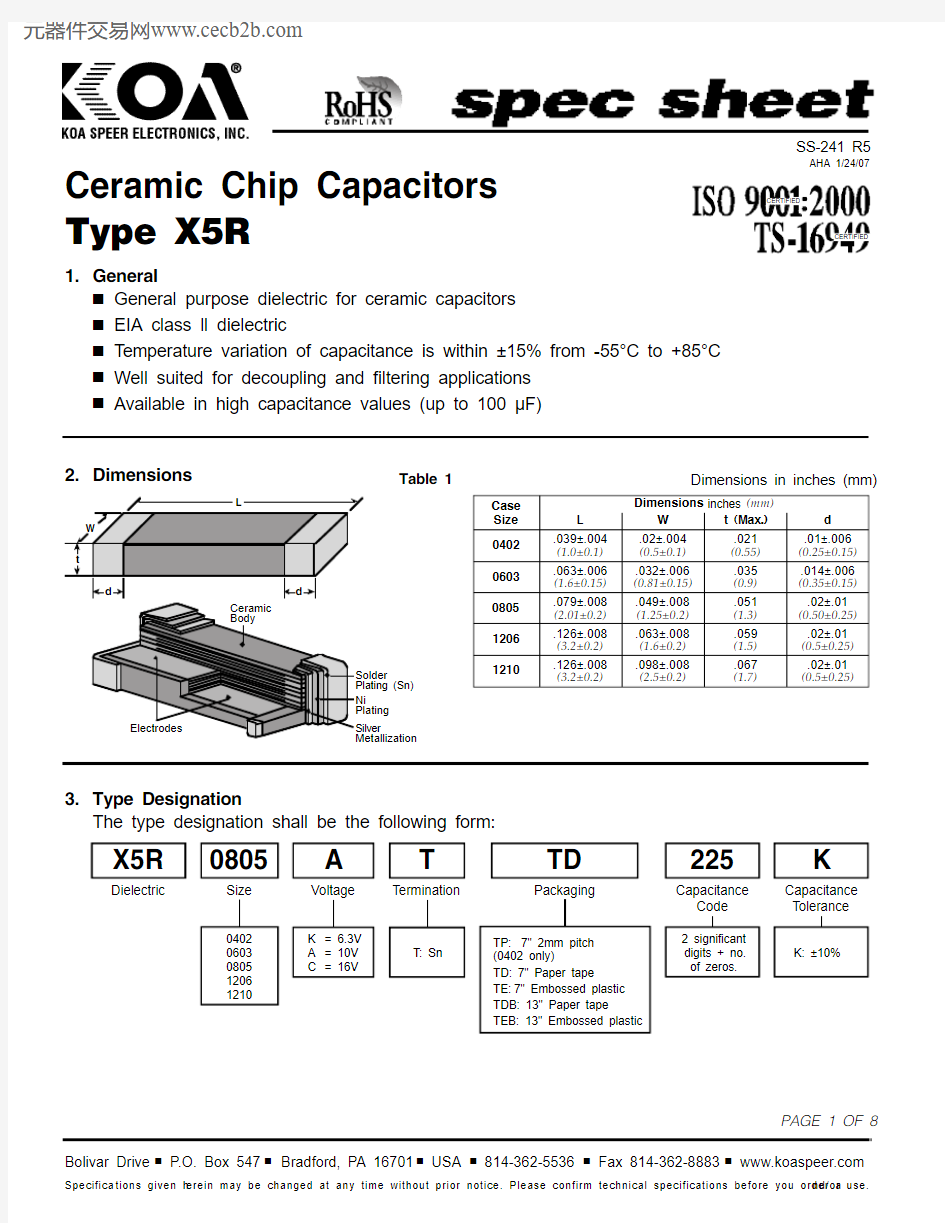
3.Type Designation
The type designation shall be the following form:
Capacitance
X5R225
Capacitance
K Dielectric
A TD
Table 1
2.Dimensions Dimensions in inches (mm)
T
CERTIFIED
SS-241 R5
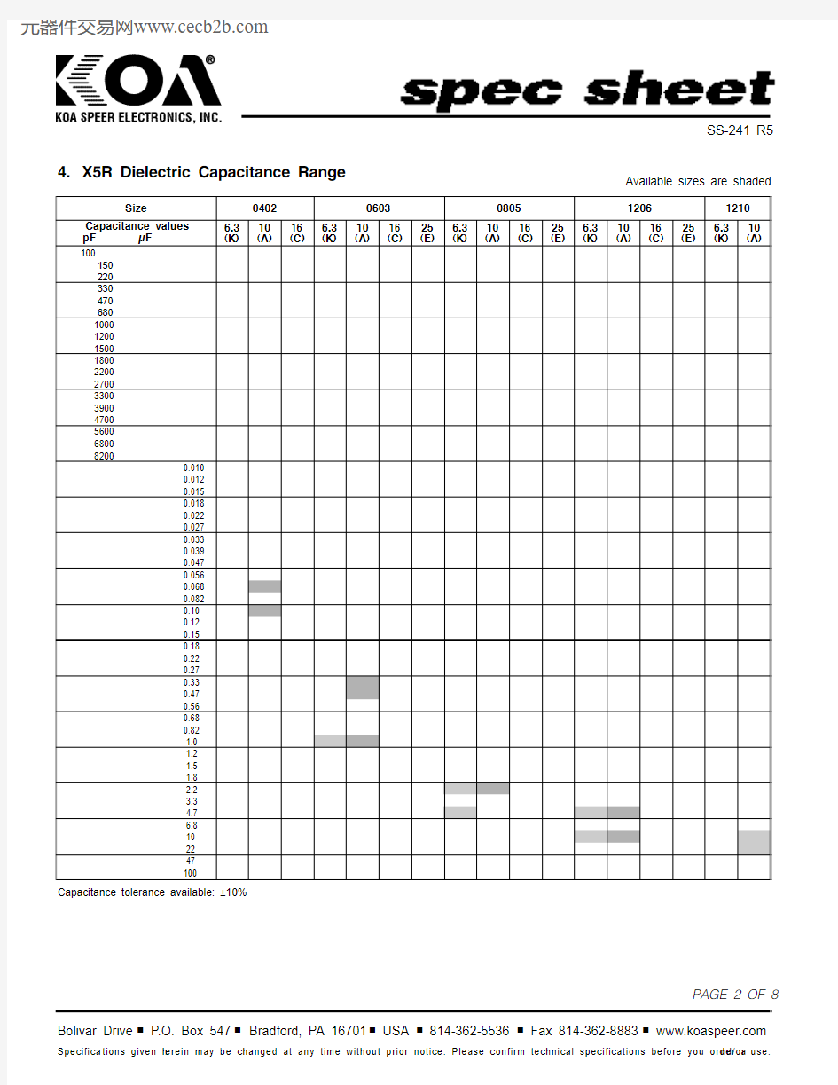
4.X5R Dielectric Capacitance Range
Available sizes are shaded.
Capacitance tolerance available: ±10%
SS-241 R5
5.Characteristics
SS-241 R5
5.Characteristics (continued)
6.Typical Impedance Characteristics
Temperature (°C)
Temperature (°C)
Insulation Resistance vs Temp. X5R - Temperature Coefficient
SS-241 R5
Metric dimensions will govern.
English measurements rounded and for reference only.
8.
* Drive spokes optional. If used, asterisked dimensions apply.
1 (Measured at hub).
for tape start.
0.98 (2.5) min. width,.394 (10) min. depth.
2 (Measured at hub).
3 (Includes flange
Dimensions in inches (mm)
7.Tape and Reel Quantities
All tape and reel specifications are in compliance with RS481.
*TP is a 7" reel with a 2mm pitch, TD & TE are 7" reels, TDB & TEB are 13" reels
Notes:
1.A 0, B 0 and K 0are determined by the max. dimensions to the ends of the terminals extending from the components body and/or the body of the component. The clearance between the end of the terminals of the body of the components to the sides and depth of the cavity (A 0, B 0and K 0) must be within .002" (0.05)mm min. and .020" (0.50)mm max. The clearance allowed must also prevent rotation of the component within the cavity of not more than 20 degrees (see examples A & B).
2.Tape with components shall pass around radius "R" without damage. The minimum trailer length (Note 2 Fig. 3) may require additional length to provide R min. for .472" (12)mm embossed tape for reels with hub diameters approaching N min. (Table 4).
3.G 1dimension is the flat area from the edge of the sprocket hole to either the outward deformation of the carrier tape between the embossed cavities or to the edge of the cavity whichever is less.
4.G 2dimension is the flat area from the edge of the carrier tape opposite the sprocket holes to either the outward deformation of the carrier tape between the embossed cavity or to the edge of the cavity whichever is less.
Dimensions in inches (mm)
SS-241 R5
9.Carrier Tape Specifications
Embossed plastic 8 & 12mm
only including draft concentric around B 0
size, see note 1
.079 x .047 (2.0 x 1.2)and larger
G 1
See note 3
See note 4
G 2
Maximum Component Rotation Side or Front Sectional View
Example "A"
T op View Example "B"
10.Carrier Tape Specifications
Punched paper tape
8 & 12mm
tape
1
SS-241 R5
Notes:
5.The embossed hole location shall be measured from the sprocket hole controlling the location of the embossment. Dimensions of embossment location and hole location shall be applied independent of each other.
6. B 1dimension is a reference dimension for tape feeder clearance only.
9.Carrier Tape Specifications (continued)
Embossed plastic 8 & 12mm
SS-241 R5
Notes:
1.A 0, B 0 and T are determined by the max. dimensions to the ends of the terminals extending from the component body and/or the body dimensions of the component. The clearance between the ends of the terminals or body of the components to the sides and depth of the cavity (A 0, B 0
within the cavity of not more than 20 degrees (see examples C & D).
2.
3..063" (1.6) mm max. for Side or Front Sectional View
Example "C"
Top View Example "D"
Side or Front Sectional View
Example "C"10.Carrier Tape Specifications (continued)
Punched paper tape 8 & 12mm
11.Recommended Land Pattern Dimensions
Component pads should be designed to achieve good solder filets and minimize component movement during reflow soldering.
Pad dimensions are given below for multilayer ceramic capacitors for both reflow and wave soldering. The basis for these designs is:
?Pad width equal to component width. It is permissible to decrease this to as low as 85% of component width but it is not advisable to go below this.?Pad overlap 0.5mm beneath component
?Pad extension 0.5mm beyond components for reflow and 1.0mm for wave soldering