FMS6203_0611中文资料
FMS6203 Low-Cost 3-Channel Video Filter Driver for SD/PS/HD November 2006
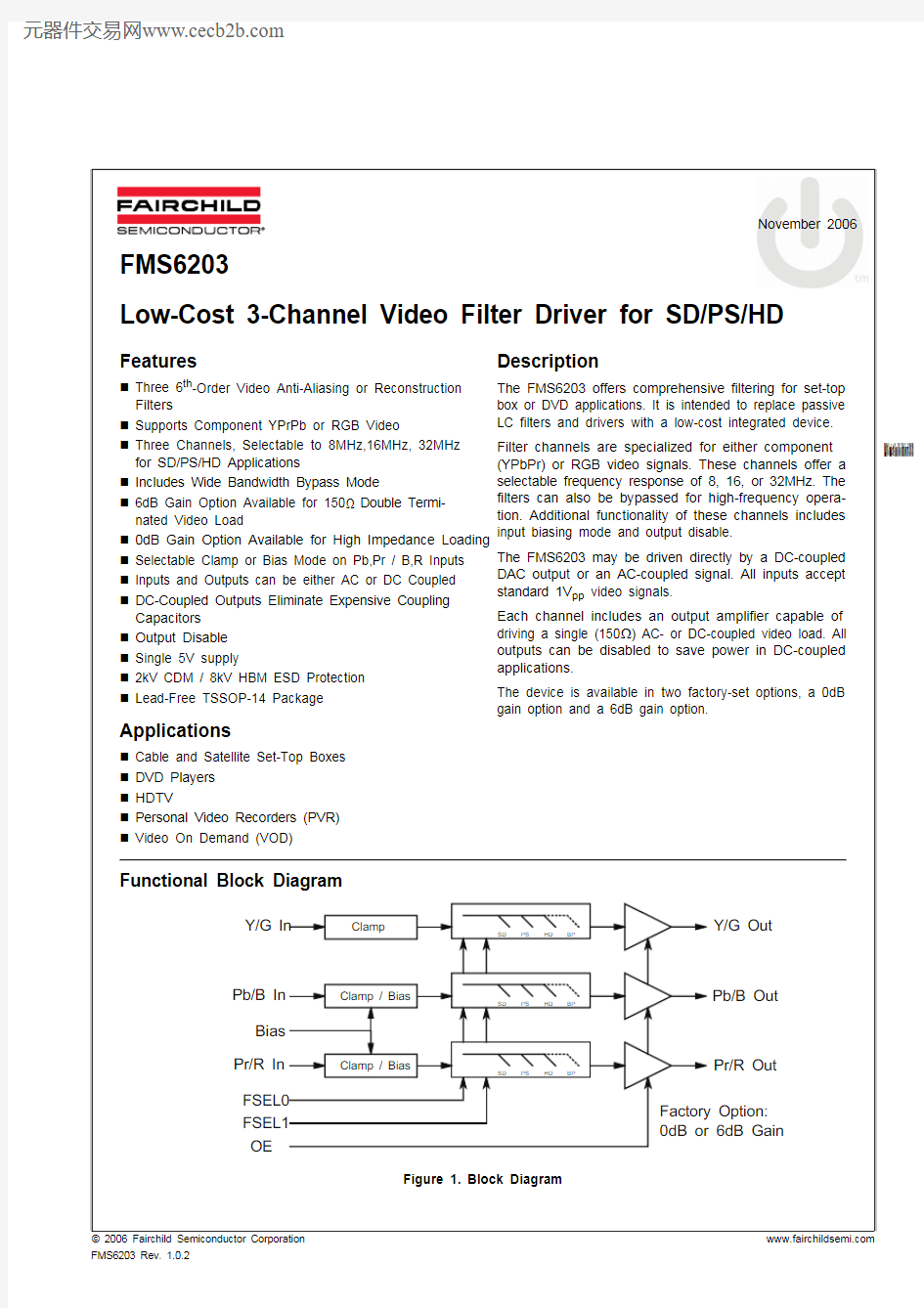
FMS6203 Low-Cost 3-Channel Video Filter Driver for SD/PS/HD
FMS6203 Low-Cost 3-Channel Video Filter Driver for SD/PS/HD
Absolute Maximum Ratings
The “Absolute Maximum Ratings” are those values beyond which the safety of the device cannot be guaranteed. The device should not be operated at these limits. The parametric values defined in the Electrical Characteristics tables are not guaranteed at the absolute maximum ratings. The “Recommended Operating Conditions” table defines the conditions for actual device operation.
Reliability Information
Recommended Operating Conditions
Parameter
Min.
Max.
Unit
DC Supply Voltage -0.36V Analog and Digital I/O
-0.3
V cc + 0.3V Output Current, Any One Channel, Do Not Exceed
50
mA
Symbol
Parameter Min.Typ.Max.
Unit
T J Junction Temperature 150°C T STG Storage Temperature Range
-65
150°C T L Lead Temperature, Soldering 10 seconds
300
°C ΘJA
Thermal Resistance JEDEC Standard Multi-Layer Test Boards, Still Air
97
°C/W
Symbol
Parameter
Min.
Typ.
Max.
Unit
T A Operating Temperature Range
-4085°C V CC
Supply Voltage Range
4.75
5.0
5.25
V
FMS6203 Low-Cost 3-Channel Video Filter Driver for SD/PS/HD
DC Electrical Characteristics
T A = 25°C, V cc = 5V, R source = 37.5Ω, inputs AC coupled with 0.1μF, all outputs AC coupled with 220μF into 150Ωloads, referenced to 400kHz; all gain options; unless otherwise noted.
Note:
1. 100% tested at 25°C.
Standard Definition Electrical Characteristics
T A = 25°C, V IN = 1V pp , V cc = 5V, R source = 37.5Ω, all inputs AC coupled with 0.1μF, all outputs AC coupled with 220μF into 150Ω loads, referenced to 400kHz, all gain options; unless otherwise noted.
Notes:
1. 100% tested at 25°C.
2. SNR = 20 * log (714mV / rms noise).
Symbol
Parameter
Conditions
Min.Typ.
Max
Units
I CC Supply Current (1)No Load
3675mA I CC1Supply Current (1)No Load, Output Disabled 1535mA V IN Video Input Voltage Range Referenced to GND if DC Coupled
1.0
V pp V IL Digital Input Low (1)F SEL0,F SEL100.8V V IH Digital Input High (1)F SEL0,F SEL1 2.4
V cc
V t ENABLE
Output Enable Time
150Ω DC load
300
ns
Symbol
Parameter
Conditions Min.
Typ.
Max
Units
AV SD Channel Gain Error (1)-0.400.4
dB f 1dBSD -1dB Bandwidth (1) 5.20
7.15MHz f cSD -3dB Bandwidth 8
MHz f SBSD Attenuation (Stopband Reject)(1) f = 27MHz
4050dB DG Differential Gain 0.3%DP Differential Phase 1.0
°THD Total Harmonic Distortion, Output
V OUT = 1.4V pp , 3.58MHz 0.6%X TALKSD Crosstalk (ch-to-ch)1MHz
-70dB SNR Signal-to-Noise Ratio (2)NTC-7 weighting, 100kHz to 4.2MHz 75dB t pdSD Propagation Delay
Delay from input to output, 4.5MHz
85
ns
FMS6203 Low-Cost 3-Channel Video Filter Driver for SD/PS/HD
Progressive Scan Electrical Characteristics
T A = 25°C, V IN = 1V pp , V cc = 5V, R source = 37.5Ω, all inputs AC coupled with 0.1μF, all outputs AC coupledwith 220μF into 150Ω loads, referenced to 400kHz, all gain options; unless otherwise no ted.
Notes:
1. 100% tested at 25°C.
2. SNR = 20 * log (714mV / rms noise).
High-Definition Electrical Characteristic
T A = 25°C, V IN = 1V pp , V cc = 5V, R source = 37.5Ω, all inputs AC coupled with 0.1μF, all outputs AC coupled with 220μF into 150Ω loads, referenced to 400kHz, all gain options; unless otherwise noted .
Notes:
1. 100% tested at 25°C.
2. SNR = 20 * log (714mV / rms noise).
Symbol
Parameter
Conditions Min.
Typ.
Max
Units
AV PS Channel Gain Error (1)-0.400.4
dB f 1dBSPS -1dB Bandwidth (1) 10.0
13.5MHz f cPS -3dB Bandwidth 16
MHz f SBPS Attenuation (Stopband Reject)(1)
f = 54MHz
3744dB THD Total Harmonic Distortion,
Output
V OUT = 1.4V pp , 7MHz
0.55%X TALKPS Crosstalk (ch-to-ch)1MHz
-75dB SNR Signal-to-Noise Ratio (2)Unweighted; 100kHz to 15MHz 66dB t pdPS
Propagation Delay
Delay from input to output, 10MHz
47
ns
Symbol
Parameter
Conditions Min.
Typ.
Max.
Units
AV HD Channel Gain Error (1)-0.400.4
dB f 1dBHD -1dB Bandwidth (1)28
31MHz f cHD -3dB Bandwidth 32
MHz f SBHD
Attenuation (Stopband Reject)(1)
f = 74.25MHz 3040dB THD
Total Harmonic Distortion, Output V OUT = 0.7V pp , 22MHz, 0dB, 10k Ω
load 0.5%V OUT = 1.4V pp , 22MHz, 6dB, 150Ω
load 0.5%X TALKHD Crosstalk (ch-to-ch)1MHz -75dB 30MHz
-57dB SNR Signal-to-Noise Ratio (2)Unweighted, 100kHz to 30MHz 66dB t pdHD Propagation Delay
Delay from input to output, 20MHz
25
ns
FMS6203 Low-Cost 3-Channel Video Filter Driver for SD/PS/HD
Bypass Mode Electrical Characteristics
T A = 25°C, V IN = 1V pp , V cc = 5V, R source = 37.5Ω, all inputs AC coupled with 0.1μF, all outputs AC coupled with 220μF into 150Ω loads, referenced to 400kHz, all gain options; unless otherwise noted.
Notes:
1. 100% tested at 25°C.
2. SNR = 20 * log (714mV / rms noise).
Frequency Select Truth Table
Symbol
Parameter
Conditions Min.
Typ.
Max.
Units
AV BP Channel Gain Error (1)DC
-0.4
00.4
dB f 1dBBP -1dB Bandwidth 90MHz f cBP -3dB Bandwidth 115
MHz THD Total Harmonic Distor-tion, Output V OUT = 0.7V pp , 22MHz, 0dB, 10k Ω load 0.3%V OUT = 1.4V pp , 22MHz, 6dB, 150Ω load 0.25%X TALKBP Crosstalk (ch-to-ch)
1MHz -74dB 30MHz
-64dB SNR Signal-to-Noise Ratio (2)Unweighted, 100kHz to 30MHz
70
dB
F SEL1
F SEL0
Filter Frequency
Video Format
Sync Format
008MHz SD,480i Bi-level, 4.7μs pulse width 0116MHz PS,480p Bi-level, 2.35μs pulse width 1032MHz HD,1080i,720p
Tri-level, 589ns pulse width
1
1
Bypass
Layout Considerations
General layout and supply bypassing play a major role in high-frequency performance and thermal characteristics. Fairchild offers a demonstration board to guide layout and aid device evaluation. The demo board is a four-layer board with full power and ground planes. Following this layout configuration provides optimum performance and thermal characteristics for the device. For the best results, follow the steps and recommended routing rules listed below.
Recommended Routing/Layout Rules
Do not run analog and digital signals in parallel.
Use separate analog and digital power planes to supply power.
Traces should run on top of the ground plane at all-times.
No trace should run over ground/power splits.
Avoid routing at 90-degree angles.
Minimize clock and video data trace length differ-ences.
Include 10μF and 0.1μF ceramic power supply bypass capacitors.
Place the 0.1μF capacitor within 0.1 inches of the device power pin.
Place the 10μF capacitor within 0.75 inches of the device power pin.
For multilayer boards, use a large ground plane to help dissipate heat. For two-layer boards, use a ground plane that extends beyond the device body by at least 0.5 inches on all
sides. Include a metal paddle under the device on the
top layer.
Minimize all trace lengths to reduce series inductance. Thermal Considerations
Since the interior of most systems, such as set-top-boxes, TVs, and DVD players are at +70oC; consider-
ation must be given to providing an adequate heat sink
for the device package for maximum heat dissipation.
When designing a system board, determine how much
power each device dissipates. Ensure that devices of
high power are not placed in the same location, such as
directly above (top plane) and below bottom plane) each
other on the PCB.
PCB Thermal Layout Considerations
Understand the system power requirements and envi-ronmental conditions.
Maximize thermal performance of the PCB.
Consider using 70μm of copper for high-power
designs.
Make the PCB as thin as possible by reducing FR4 thickness.
Use vias in power pad to tie adjacent layers together.
Remember that baseline temperature is a function of board area, not copper thickness.
Modeling techniques can provide a first-order approxi-
FMS6203 Low-Cost 3-Channel Video Filter Driver for SD/PS/HD
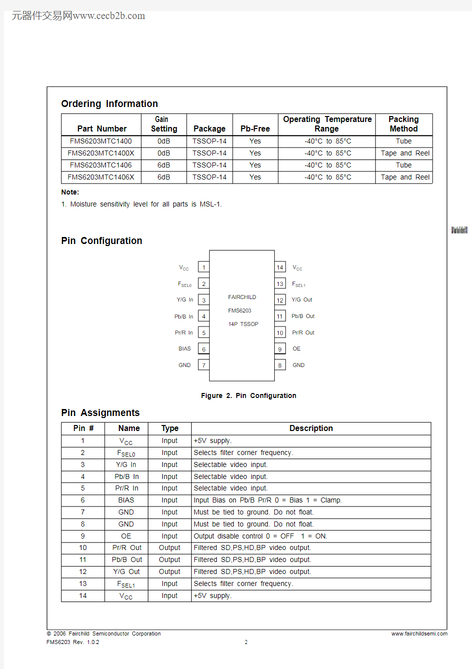
FMS6203 Low-Cost 3-Channel Video Filter Driver for SD/PS/HD
FMS6203 Low-Cost 3-Channel Video Filter Driver for SD/PS/HD