20.8-inch WXGA Full Color AMOLED Display by Integrating Scattering Reflector with Micro-Bumps
13.4 / S. Okutani
13.4: A 20.8-inch WXGA Full Color AMOLED Display by Integrating
Scattering Reflector with Micro-Bumps
Satoshi Okutani, Norihiko Kamiura, Hiroshi Sano, Takumi Sawatani, Daisuke Fujita,
Toshifumi Takehara, Kazuyuki Sunohara, and Michiya Kobayashi
Research & Development Center, Toshiba Matsushita Display Technology Co., Ltd.
26-2, Kawakita, Nomi, Ishikawa 923-1296, Japan
Nobuki Ibaraki
Toshiba Matsushita Display Technology Co., Ltd.
Rivage Shinagawa, 4-1-8, Konan, Minato-ku, Tokyo 180-0075, Japan
Abstract
In order to improve light extraction efficiency from organic light emitting diodes (OLED), we report a novel structure of top-emission OLED by integrating a scattering reflector with micro-bumps into the substrate. The mechanism of light extraction has been investigated by evaluating the dependency of flux on the shape of the micro-bumps. It was confirmed that the scattering effect of the micro-bumps improves the light extraction of OLED. Moreover, the scattering reflector has been applied on a 20.8-inch WXGA full color AMOLED display. This is the world's first report that actually proves a light extraction technology, integrating scattering reflector, applied on AMOLED display.
1. Introduction
Organic light emitting diode (OLED) displays are one of the most promising next generation flat panel displays on account of their several advantages such as high contrast ratio, extremely fast response, very wide viewing angle, and simple structure. Recently, active-matrix OLED (AMOLED) displays, using thin film transistor (TFT) backplane, have been developed for pursuing higher resolution and lower power consumption [1][2][3][4][5]. However, the problems on power consumption and lifetime, especially for large-scale TV applications, have not been solved. A breakthrough is needed to improve light extraction efficiency. Although several novel structures have been reported in order to effectively extract the light from the OLED emission layer, there are few reports that have been applied to actual display [6][7][8][9][10][11][12], due to the complexity of the structure, procedures, and the limitation of the fabrication area. It is also because of a double-image attributed to the parallax effect in bottom-emission OLED displays.
In this paper, we propose a novel light extraction structure of OLED, which can be easily applied to an actual AM-OLED to improve the light extraction. The mechanisms of the scattering reflector are discussed. Moreover, AMOLED display integrating the scattering reflector is demonstrated.
2. Principles
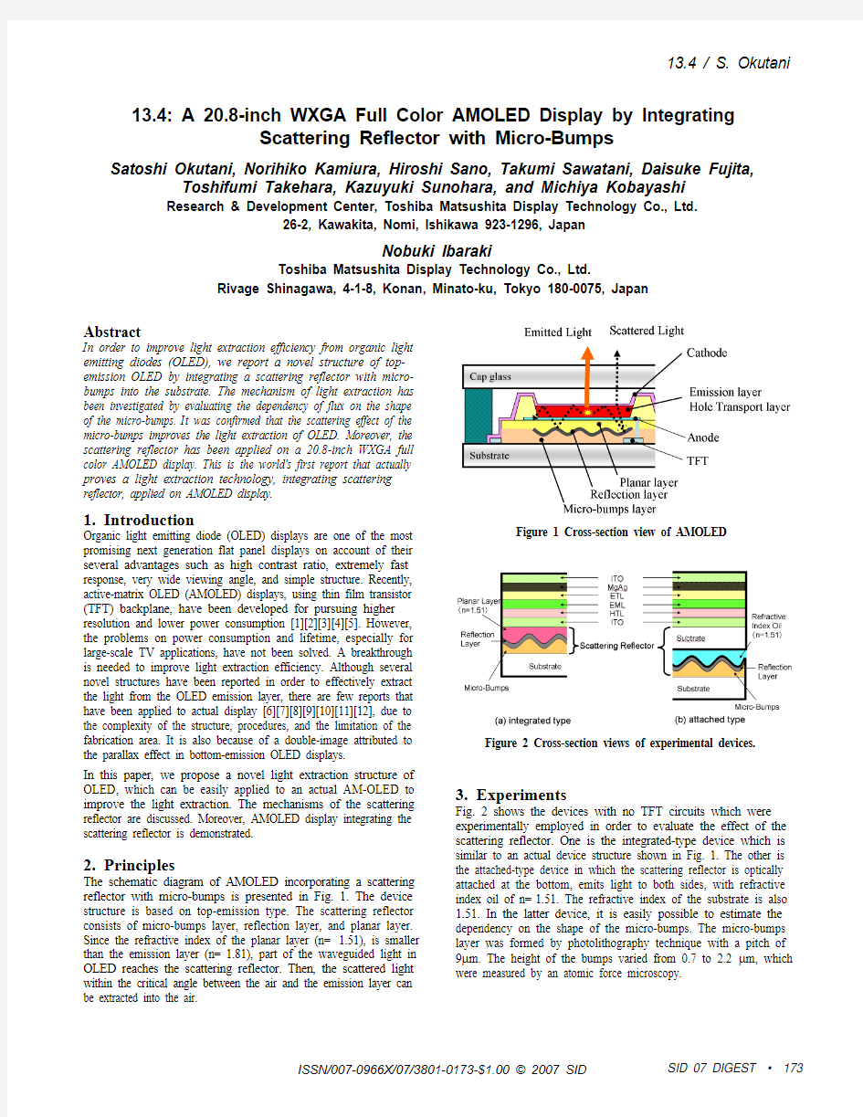
The schematic diagram of AMOLED incorporating a scattering reflector with micro-bumps is presented in Fig. 1. The device structure is based on top-emission type. The scattering reflector consists of micro-bumps layer, reflection layer, and planar layer. Since the refractive index of the planar layer (n=1.51), is smaller than the emission layer (n=1.81), part of the waveguided light in OLED reaches the scattering reflector. Then, the scattered light within the critical angle between the air and the emission layer can
be extracted into the air.
Figure 1 Cross-section view of AMOLED
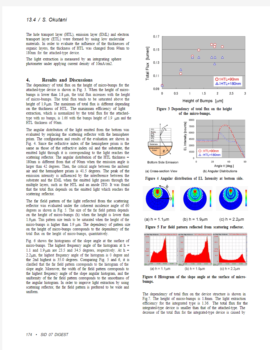
Figure 2 Cross-section views of experimental devices.
3. Experiments
Fig. 2 shows the devices with no TFT circuits which were experimentally employed in order to evaluate the effect of the scattering reflector. One is the integrated-type device which is similar to an actual device structure shown in Fig. 1. The other is the attached-type device in which the scattering reflector is optically attached at the bottom, emits light to both sides, with refractive index oil of n=1.51. The refractive index of the substrate is also 1.51. In the latter device, it is easily possible to estimate the dependency on the shape of the micro-bumps. The micro-bumps layer was formed by photolithography technique with a pitch of 9μm. The height of the bumps varied from 0.7 to 2.2μm, which were measured by an atomic force microscopy.
SID 07 DIGEST ? 173
ISSN/007-0966X/07/3801-0173-$1.00 ? 2007 SID
13.4 / S. Okutani
The hole transport layer (HTL), emission layer (EML) and electron transport layer (ETL) were formed by using low molecular materials. In order to evaluate the influence of the thicknesses of organic layers, the thickness of HTL was changed from 90nm to 180nm for the attached-type device.
The light extraction is measured by an integrating sphere photometer under applying current density of 10mA/cm2.
4. Results and Discussions
The dependency of total flux on the height of micro-bumps for the attached-type device is shown in Fig. 3. When the height of micro-bumps is lower than 1.8μm, the total flux increases with the height of micro-bumps. The total flux tends to be saturated above the height of 1.9μm. The maximum of total flux is different depending on the thickness of HTL. The maximum efficiency of light extraction, which is normalized by the total flux for the attached-type with no bumps, is 1.66 with the bumps height of 1.9μm and the HTL thickness of 90nm.
The angular distribution of the light emitted from the bottom was evaluated by replacing the scattering reflector with the hemisphere prism. The configuration and results of the evaluation are shown in Fig. 4. Since the refractive index of the hemisphere prism is the same as those of the refractive index oil and the substrate, the emitted light through it is corresponding to the light reaches the scattering reflector. The angular distribution of the HTL thickness = 180nm is different from that of 90nm when the emission angle is larger than 42 degrees. Then, the critical angle between the ambient air and the hemisphere prism is 41.5 degrees. The peak of the emission intensity is influenced by the interference between the substrate and the EML when the emitted light passes through the multiple layers, such as the HTL and an anode ITO. It was found that the total flux depends on the emitted light which reaches the scattering reflector.
The far field pattern of the light reflected from the scattering reflector was evaluated under the coherent incidence angle of 60 degrees as shown in Fig. 5. The size of the far field pattern depends on the height of micro-bumps (h) when the height is lower than 1.9μm. This pattern size tends to be saturated when the height of the micro-bumps is higher than 1.9μm. The dependency of pattern size on the height of micro-bumps corresponds to the dependency of the total flux on the height of micro-bumps, quantitatively.
Fig. 6 shows the histograms of the slope angle at the surface of micro-bumps. The highest frequency angle of the histogram at h = 1.1 and 1.9μm are 23.5 and 34.5 degrees, respectively. At h = 2.2μm, the highest frequency angle of the histogram is 0 degree and the 2nd highest is 35.0 degrees. Comparing Fig. 5 and 6, it is clarified that the far field pattern corresponds to the histogram of the slope angle. Moreover, the width of far field pattern corresponds to the highest frequency angle of the slope angular histogram, and the uniformity of the far field pattern corresponds to the smoothness of the angular histogram. In order to improve light extraction by using scattering reflector, the far field pattern is preferred to be wide and
uniform.
Figure 3 Dependency of total flux on the height
of the micro-bumps.
Figure 4 Angular distribution of EL Intensity at bottom side.
Figure 5 Far field pattern reflected from scattering reflector.
Figure 6 Histogram of the slope angle at the surface of micro-bumps.
The dependency of total flux on the device structure is shown in Fig.7. The height of micro-bumps is 1.8mm. The light extraction efficiency for the integrated type is 1.36. The total flux for the integrated-type device is smaller than that of the attached-type. The decrease of the total flux for the integrated-type device is caused by
174 ? SID 07 DIGEST
13.4 / S. Okutani
the absorption at the planar layer as it is formed by using the photo-resist resin.
The dependency of the total flux on the thickness of the planar layer is shown in Fig.8. It was confirmed that the absorption of the planar layer can not be neglected. The scattering reflector should consist of lower absorption materials.
5. 20.8-inch AMOLED
Table 1 shows the specification of a 20.8-inch AMOLED display integrating the scattering reflector with micro-bumps. The backplane of the display is a low temperature poly-Si TFT array. The device structure is top-emission type. In order to achieve full color capability, the light emitting layers are selectively ink-jetted equivalent to RGB pixels. The circular polarizer is attached on the panel in order to prevent reflection of outside light.
A picture image on the 20.8-inch AMOLED display is shown in Fig. 9. The dependency of colors on viewing angle, which is often caused by the micro-cavity effect, is not observed on this display. Moreover, the contrast ratio of OLED is retained under bright ambient conditions. As the scale of micro-bumps is much larger than wavelength, the polarization state of light which reflected from the scattering reflector is maintained. There is no double-image attributed to the parallax. Although the device structure, including the shape of micro-bumps and thickness of organic layers, has not been optimized, it was confirmed that the scattering reflector with micro-bumps is a technology applicable on an actual display.
6. Conclusion
We have studied the effects of the scattering reflector integrated in OLED with the aim of increasing its extraction efficiency. The light extraction efficiencies of the integrated-type and attached-type were 1.36 and 1.66, respectively. Further improvement can be achieved by optimizing the shape of micro-bumps and applying lower absorption materials to the scattering reflector.
A 20.8-inch WXGA full color AMOLED integrating scattering reflector has been developed. This is the world's first study that actually proves a light extraction technology, integrating scattering reflector, applied on AMOLED display.
7. Acknowledgements
A part of this work belongs to “Advanced Organic Device Project” which OITDA contracted with New Energy and Industrial
Technology Development Organization (NEDO).
Figure 7 Dependency of total flux on device structures.
Figure 8 Dependency of total flux on thickness of planar layer.
Table 1 Specification of 20.8-inch OLED display
Figure 9 Picture image of 20.8-inch OLED display .
8. References
[1] M. Kobayashi, J. Hanari, M. Shibusawa, K. Sunohara, and N.
Ibaraki, “A 17-in. WXGA full-color OLED display by using polymer ink-jet technology ” IDW2002 Proceeding, pp231-234, (2002) [2] G. Rajeswaran, M. Itoh, M. Boroson, S. Barry, T. K. Hatwar,
K. B. Kahen, K. Yoneda, R. Yokoyama, T. Yamada, N. Komiya, H. Kannoand, and H. Takahashi, “Active Matrix Low Temperature Poly-Si TFT / OLED Full Color Displays : Development Status” SID2000 Technical Digest, pp.974, (2000)
SID 07 DIGEST ? 175
13.4 / S. Okutani
[3]T. Sasaoka, M. Sekiya, A. Yumoto, J. Yamada, T. Hirano, Y.
Iwase, T.Yamada, T. Ishibashi, T. Mori, M. Asano, S.
Tamura, and T. Urabe, “A 13.0-inch AM-OLED display with top emitting structure and adaptive current mode programmed pixel circuit (TAC) ” SID2001 Technical Digest, pp.384-387, (2001)
[4]T. Funamoto, Y .Matsueda, O. Yokoyama, A. Tsuda, H.
Takeshita, and S. Miyashita, “A 130-ppi full-color polymer
OLED display” SID 2002 Digest, pp.889-901, (2002)
[5]H. K. Chung, “High efficiency active matrix organic LED”
IDW2002, pp.1107-1110, (2002)
[6] C. F. Madigan, M.-H. Lu, and J. C. Sturm, “Improvement of
output coupling efficiency of organic light-emitting diodes by backside substrate modification” Appl. Phys. Lett.
76,1650,(2000)
[7]J. J. Shiang, T. J. Faircloth, and Anil R. Duggal, “Application
of radiative transport theory to light extraction from organic
light emitting diodes” J. Appl. Phys. 95, 2889 (2004)
[8]T. Nakamura, N. Tsutsumi, N. Juni and H. Fujii, “Thin-film
waveguiding mode light extraction in organic
electroluminescent device using high refractive index
substrate” J. Appl. Phys. 97, 97 (2005)
[9]J. M. Lupton, B. J. Matterson, and I. D. W. Samuel,“Bragg
scattering from periodically microstructured light emitting
diodes”Appl. Phys. Lett. 77,3340,(2000)
[10]T. Tsutsui, M. Yahiro, H. Yokogawa, K. Kawano, and M.
Yokoyama, “Doubling Coupling-Out Efficiency in Organic
Light-Emitting Devices Using a Thin Silica Aerogel Layer”
Adv. Mater. 15, 1149, (2001)
[11]Y. J. Lee, S. H. Kim, J. Huh, G. H. Kim, Y. H. Lee, S. H.
Cho, Y. C. Kim, and Y. R. Do, “A high-extraction-
efficiency nanopatterned organic light-emitting diode”
Appl. Phys. Lett. 82,3779,(2003)
[12]M. Kitamura, S. Iwamoto and Y. Arakawa, “Enhanced
Luminance Efficiency of Organic Light-Emitting Diodes with Two-Dimensional Photonic Crystals” Jpn. J. Appl. Phys. 44
2844 (2005)
176 ? SID 07 DIGEST