ADS1252EVM;中文规格书,Datasheet资料
DESCRIPTION
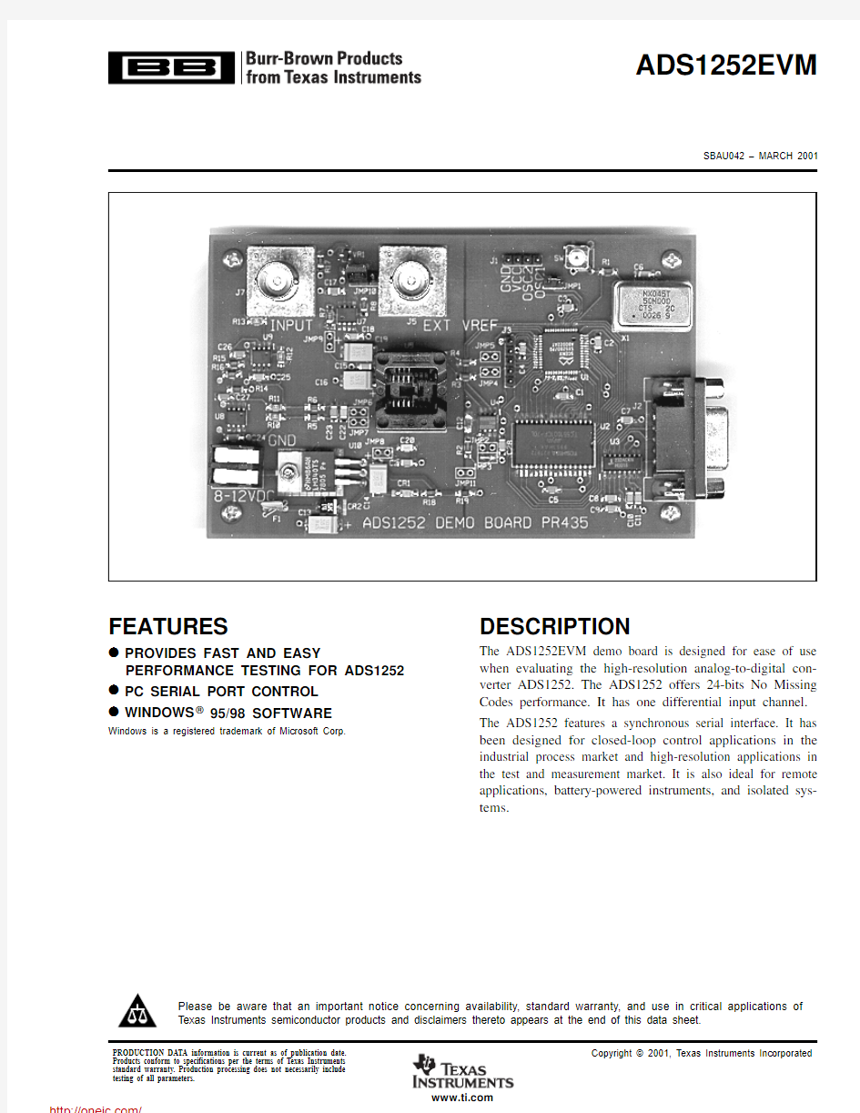
The ADS1252EVM demo board is designed for ease of use when evaluating the high-resolution analog-to-digital con-verter ADS1252. The ADS1252 offers 24-bits No Missing Codes performance. It has one differential input channel.The ADS1252 features a synchronous serial interface. It has been designed for closed-loop control applications in the industrial process market and high-resolution applications in the test and measurement market. It is also ideal for remote applications, battery-powered instruments, and isolated sys-tems.
FEATURES
q PROVIDES FAST AND EASY
PERFORMANCE TESTING FOR ADS1252q PC SERIAL PORT CONTROL q WINDOWS ? 95/98 SOFTWARE
Windows is a registered trademark of Microsoft Corp.
ADS1252EVM
SBAU042 – MARCH 2001
https://www.360docs.net/doc/289569914.html,
PRODUCTION DATA information is current as of publication date.Products conform to specifications per the terms of Texas Instruments standard warranty. Production processing does not necessarily include testing of all parameters.
Copyright ? 2001, Texas Instruments Incorporated
Please be aware that an important notice concerning availability, standard warranty, and use in critical applications of
Texas Instruments semiconductor products and disclaimers thereto appears at the end of this data sheet.
https://www.360docs.net/doc/289569914.html,/
ADS1252EVM
2
SBAU042
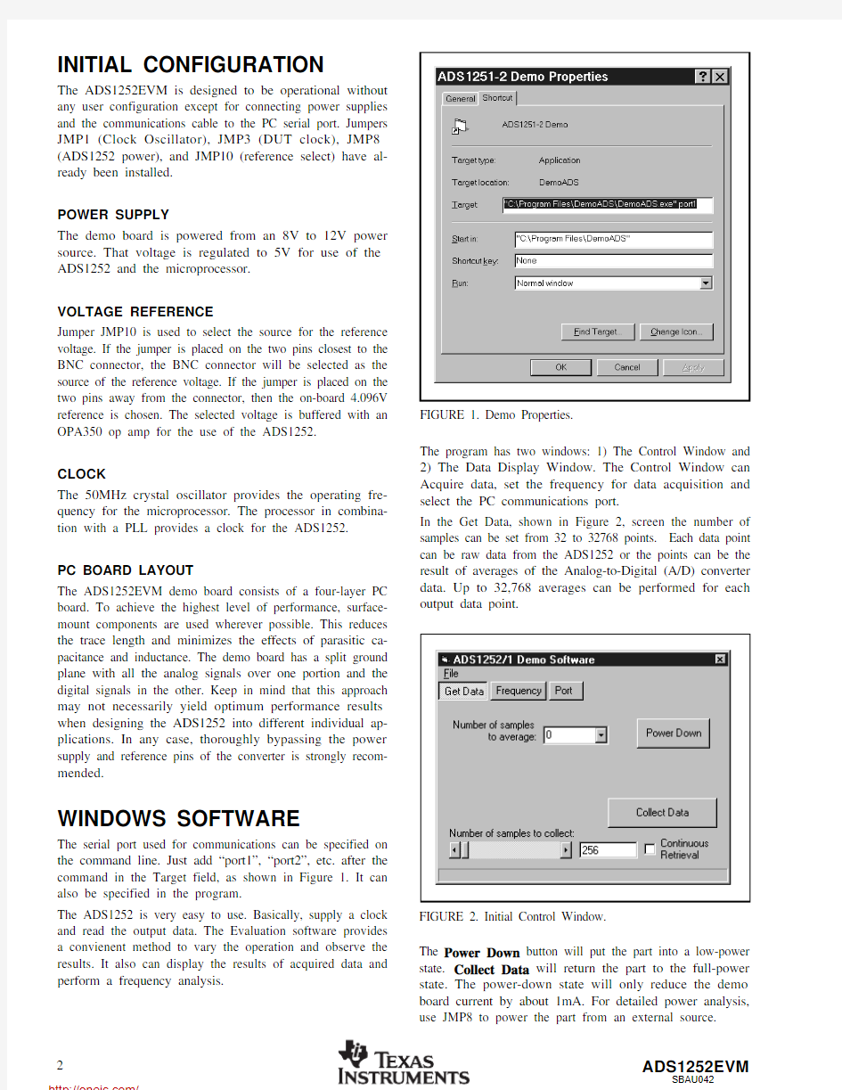
FIGURE 1. Demo Properties.
FIGURE 2. Initial Control Window.
INITIAL CONFIGURATION
The ADS1252EVM is designed to be operational without any user configuration except for connecting power supplies and the communications cable to the PC serial port. Jumpers JMP1 (Clock Oscillator), JMP3 (DUT clock), JMP8(ADS1252 power), and JMP10 (reference select) have al-ready been installed.POWER SUPPLY
The demo board is powered from an 8V to 12V power source. That voltage is regulated to 5V for use of the ADS1252 and the microprocessor.VOLTAGE REFERENCE
Jumper JMP10 is used to select the source for the reference voltage. If the jumper is placed on the two pins closest to the BNC connector, the BNC connector will be selected as the source of the reference voltage. If the jumper is placed on the two pins away from the connector, then the on-board 4.096V reference is chosen. The selected voltage is buffered with an OPA350 op amp for the use of the ADS1252.CLOCK
The 50MHz crystal oscillator provides the operating fre-quency for the microprocessor. The processor in combina-tion with a PLL provides a clock for the ADS1252.PC BOARD LAYOUT
The ADS1252EVM demo board consists of a four-layer PC board. To achieve the highest level of performance, surface-mount components are used wherever possible. This reduces the trace length and minimizes the effects of parasitic ca-pacitance and inductance. The demo board has a split ground plane with all the analog signals over one portion and the digital signals in the other. Keep in mind that this approach may not necessarily yield optimum performance results when designing the ADS1252 into different individual ap-plications. In any case, thoroughly bypassing the power supply and reference pins of the converter is strongly recom-mended.
WINDOWS SOFTWARE
The serial port used for communications can be specified on the command line. Just add “port1”, “port2”, etc. after the command in the Target field, as shown in Figure 1. It can also be specified in the program.
The ADS1252 is very easy to use. Basically, supply a clock and read the output data. The Evaluation software provides a convienent method to vary the operation and observe the results. It also can display the results of acquired data and perform a frequency analysis.
The program has two windows: 1) The Control Window and 2) The Data Display Window. The Control Window can Acquire data, set the frequency for data acquisition and select the PC communications port.
In the Get Data, shown in Figure 2, screen the number of samples can be set from 32 to 32768 points. Each data point can be raw data from the ADS1252 or the points can be the result of averages of the Analog-to-Digital (A/D) converter data. Up to 32,768 averages can be performed for each output data point.
The Power Down button will put the part into a low-power state. Collect Data will return the part to the full-power state. The power-down state will only reduce the demo board current by about 1mA. For detailed power analysis,use JMP8 to power the part from an external source.
https://www.360docs.net/doc/289569914.html,/
ADS1252EVM
SBAU042
3
FIGURE 4. Configuration Window.
FIGURE 3. Frequency Window.
The Frequency screen, shown in Figure 3, lets you choose the operating frequency of the device. The frequencies of 2kHz, 10kHz, and 35kHz give good noise performance.Although, by selecting Variable Sample Rate, other sample rates can be selected by choosing the output sample rate or the clock frequency (Sample Rate ? 384). The noise perfor-mance is not as good when using the Variable Sample Rate because of the PLL used to generate the clocks.
The Options screen, shown in Figure 4, gives you control of which serial port the program will use when it communi-cates with the evaluation module. This is also where you specify the reference voltage used to normalize the data for
a “scaled by LSB” voltage display.
FIGURE 5. Time Domain Display.
Several figures of merit are computed from the FFT infor-mation shown in Figure 6. These include the Signal to Noise Ratio (SNR), Signal to Noise plus Distortion (SINAD),Total Harmonic Distortion (THD) and Spurious Free Dy-namic Range (SFDR).
FIGURE 6. FFT Display.
Along the top of the Time Domain Display, shown in figure 5,are icons that can be used to select the various display modes. The four displays are 1) Time Domain, 2) FFT,3) Histogram, and 4) Data List. Statistics for the data are also displayed on the top of the Time Domain Display. It shows the Standard Deviation, Mean, Maximum, and Minimum.
https://www.360docs.net/doc/289569914.html,/
ADS1252EVM
4
SBAU042
FIGURE 7. FFT Options.
FIGURE 8. Data List Display.
There are many options for the FFT display. The options menu selection opens the screen shown in Figure 7.
Several windows are provided to modify the data before the FFT computation. Additionally, the FFT display can mark some features such as the main frequency and the harmon-ics.
Finally, the data can be analyzed in detail with the Data List display shown in figure 8.
The Data Formats can be selected. This selection will also be used for the display of the date in the Time Domain display.The “Scaled by LSB” converts the data to a voltage with the assumption that the voltage reference is as defined in Figure 4.
https://www.360docs.net/doc/289569914.html,/
ADS1252EVM
SBAU042
5
FIGURE 9. Schematic
https://www.360docs.net/doc/289569914.html,/
ADS1252EVM
6
SBAU042
COMPONENT LIST
PART NUMBER DESCRIPTION
REF. DES.QTY VENDOR PART NUMBER MANUFACTURER ADS1252U IC, A/D CONV, 24-BIT,20kHz U61 ADS1252U B3F-1050SWITCH, SPST, PB-MOM
SW11 B3F-1050CRCW120610R0F RES, 10.0?, 0.125W, 1%, CHIP-THICK-FILM R 191 CRCW120610R0F DALE CRCW1206000RES, 0.0?, 0.125W, 0%, CHIP-JUMPER R 5,R 6,R 173 CRCW1206000 DALE CRCW12061001F RES, 1.0k ?, 0.125W, .1%, CHIP-THICK-FILM R 18
1 CRCW12061001F DALE CRCW12061002F RES, 10.0k ?, 0.125W, 1%, CHIP-THICK-FILM R 1,R 7,R 8,R 144 CRCW12061002F DALE CRCW12062000RES, 200?, 0.125W, 1%, CHIP-THICK-FILM R 2,R 3,R 43 CRCW12062000F DALE CRCW12064991F RES, 4.99k ?, 0.125W, 1%, CHIP-THICK-FILM R 9,R 15,R 163 CRCW12064991F DALE C1206C101K5GAC CAP, 100pF, 50V, 10%, CHIP-CERAMIC COG C 12,C 20
2 C1206C101K5GAC KEMET C1206C103K5RAC CAP, .01uF, 50V, 10%, CHIP-CERAMIC X7R C 17
1 C1206C103K5RAC KEMET C1206C104K5RAC
CAP, 0.10uF, 50V, 10%, CHIP-CERAMIC X7R C 1,C 2,C 3,C 4,C 5,C 620
C1206C104K5RAC
KEMET
*C 7,C 8,C 9,C 10,C 11*C 15,C 18,C 21,C 23,C 24*
C 25,C 26,C 27,C 28C1206C221K5GAC CAP, 220pF, 50V, 10%, CHIP-CERAMIC COG C 221 C1206C221K5GAC KEMET
ICD2053BSC-1IC, PROGRAMMABLE CLOCK GENERATOR U41 ICD2053BSC-1LM4040AIM3-4.1IC, PREC. V REF 4.1V, 0.1% SOT-23
VR11 LM4040AIM3-4.1LM7805CT 3-TERM. 5V/1A POS. FIXED REGULATOR, T U101 LM7805CT National Semi MAX232ACSE IC, DRVR/RCVR, RS-232 +5V U31 MAX232ACSE OPA350UA OPAMP, CMOS, SINGLE-SUPPLY U7,U8,U93 OPA350UA OTS-(8)16-1.27-03SOCKET, SO-8 OTS16 SERIES
U51 OTS-(8)16-1.27-03
RUE090FUSE, 30V, RESETTABLE POLYSWITCH F11 RUE090SK14DIODE, SCHOTTKEY, 40PIV,1.0A CR21 SK14
SML-LX1206-GC-TR LED, SMT 1206, GREEN
CR11 SML-LX1206-GC-TR
SX52BD/PQ IC, uPROC, 4k WORD 50MHz.U11 SX52BD/PQ TC551001/CFT-70L IC, MEMORY 1Mb X 8-BIT SRAM U2
1 TC551001/CFT-70L TNPW12061001B RES 1k 1/8W .1%
R 10,R 11,R 12,R 13
4 TNPW12061001B TSW-102-07-L-S
CONN, 2 POS .1 CTR .025 SQ. POST JMP1,JMP2,JMP3,JMP410
TSW-102-07-L-S
*JMP5,JMP6,JMP7,JMP8 *
JMP9,JMP11TSW-103-07-L-S CONN, 3 POS .1 CTR .025 SQ. POST JMP101 TSW-103-07-L-S TSW-104-07-L-S CONN, 4 POS .1 CTR .025 SQ. POST J11 TSW-104-07-L-S TSW-105-07-L-S CONN, 5 POS .1 CTR .025 SQ. POST
J3
1 TSW-105-07-L-S T491D106K035AS CAP, 10uF, 35V, 10%, TANTALUM CHIP-MOLDED C 13,C 14,C 16,C 19p 4 T491D106K035AS KEMET
VF161SHHL IC, HYBRID XTAL OSC ,VERY HI SPEED
X11 VF161SHHL 2SV-02TERM. BLK, 2 POS LEVER POWER CONNECTOR J41 2SV-02227699-1CONN, JACK, BNC, PCB MNT, VERTICAL, 50?
J5,J7
2 227699-1745781-4
CONN, DB9, RECPT .318 STYLE WITH STD HDWR J2
1
745781-4
Total Parts Used: 80
https://www.360docs.net/doc/289569914.html,/
分销商库存信息: TI
ADS1252EVM