STM32原理图含保护电路

UM0723
User manual
1 kW three-phase motor control demonstration board
featuring L6390 drivers and STGP10NC60KD IGBT 1 Introduction
This document describes the 1 kW three-phase motor control demonstration board featuring
the L6390 high and low-side drivers and the STGP10NC60KD IGBT. The demonstration
board is an AC/DC inverter that generates a three-phase waveform for driving three or two-
phase motors such as induction motors or PMSM motors up to 1000 W with or without
sensors.
The main device presented in this user manual is a universal, fully evaluated, and populated
design consisting of a three-phase inverter bridge based on the 600 V STMicroelectronics?
IGBT STGP10NC60KD in a TO-220 package mounted on a heatsink, and the L6390 high-
voltage high-side and low-side driver featuring an integrated comparator for hardware
protection features such as overcurrent and overtemperature. The driver also integrates an
operational amplifier suitable for advanced current sensing. Thanks to this advanced
characteristic, the system has been specifically designed to achieve an accurate and fast
conditioning of the current feedback, therefore matching the typical requirements in field
oriented control (FOC).
The board has been designed to be compatible with single-phase mains, supplying from
90 VAC to 285 VAC or from 125 VDC to 400 VDC for DC voltage. With reconfiguration of the
input sourcing, the board is suitable also for low-voltage DC applications up to 35 VDC. This
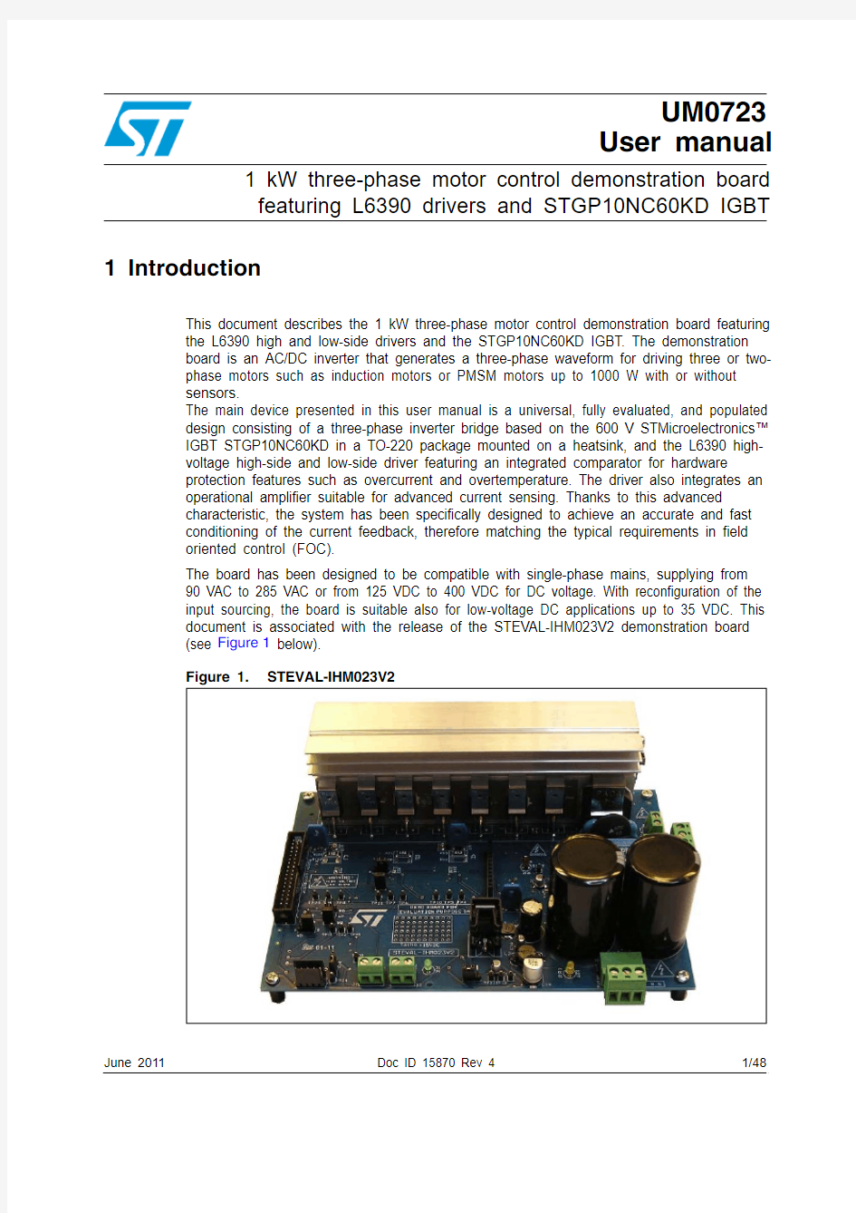
document is associated with the release of the STEVAL-IHM023V2 demonstration board
(see Figure1 below).
Figure 1.STEVAL-IHM023V2
June 2011Doc ID 15870 Rev 41/48
Contents UM0723
Contents
1Introduction . . . . . . . . . . . . . . . . . . . . . . . . . . . . . . . . . . . . . . . . . . . . . . . . 1
2System introduction . . . . . . . . . . . . . . . . . . . . . . . . . . . . . . . . . . . . . . . . . 6
2.1Main characteristics . . . . . . . . . . . . . . . . . . . . . . . . . . . . . . . . . . . . . . . . . . 6
2.2Target applications . . . . . . . . . . . . . . . . . . . . . . . . . . . . . . . . . . . . . . . . . . . 6
2.3Safety and operating instructions . . . . . . . . . . . . . . . . . . . . . . . . . . . . . . . . 7
2.3.1General terms . . . . . . . . . . . . . . . . . . . . . . . . . . . . . . . . . . . . . . . . . . . . . 7
2.3.2Demonstration board intended use . . . . . . . . . . . . . . . . . . . . . . . . . . . . . 7
2.3.3Demonstration board installation . . . . . . . . . . . . . . . . . . . . . . . . . . . . . . . 7
2.3.4Electrical connections . . . . . . . . . . . . . . . . . . . . . . . . . . . . . . . . . . . . . . . 8
2.3.5Demonstration board operation . . . . . . . . . . . . . . . . . . . . . . . . . . . . . . . . 8
3Board description . . . . . . . . . . . . . . . . . . . . . . . . . . . . . . . . . . . . . . . . . . . 9
3.1System architecture . . . . . . . . . . . . . . . . . . . . . . . . . . . . . . . . . . . . . . . . . . 9
3.2The board schematic . . . . . . . . . . . . . . . . . . . . . . . . . . . . . . . . . . . . . . . . 10
3.3Circuit description . . . . . . . . . . . . . . . . . . . . . . . . . . . . . . . . . . . . . . . . . . . 16
3.3.1Power supply . . . . . . . . . . . . . . . . . . . . . . . . . . . . . . . . . . . . . . . . . . . . . 16
3.3.2Inrush limitation . . . . . . . . . . . . . . . . . . . . . . . . . . . . . . . . . . . . . . . . . . . 17
3.3.3Brake function . . . . . . . . . . . . . . . . . . . . . . . . . . . . . . . . . . . . . . . . . . . . 17
3.3.4Gate driving circuit . . . . . . . . . . . . . . . . . . . . . . . . . . . . . . . . . . . . . . . . . 18
3.3.5Overcurrent protection . . . . . . . . . . . . . . . . . . . . . . . . . . . . . . . . . . . . . . 18
3.3.6Current sensing amplifying network . . . . . . . . . . . . . . . . . . . . . . . . . . . . 19
3.3.7The tachometer and Hall/encoder inputs . . . . . . . . . . . . . . . . . . . . . . . . 23
3.3.8Temperature feedback and overtemperature protection . . . . . . . . . . . . 23
4Hardware setting of the STEVAL-IHM023V2 . . . . . . . . . . . . . . . . . . . . . 24
4.1Hardware settings for six-step (block commutation) control of BLDC
motors . . . . . . . . . . . . . . . . . . . . . . . . . . . . . . . . . . . . . . . . . . . . . . . . . . . 24
4.2Hardware settings for “Field Oriented Control” (FOC) in single-shunt
topology current reading configuration . . . . . . . . . . . . . . . . . . . . . . . . . . . 26
4.3Hardware settings for FOC in three-shunt configuration . . . . . . . . . . . . . 27 5Description of jumpers, test pins, and connectors . . . . . . . . . . . . . . . 30
2/48Doc ID 15870 Rev 4
UM0723Contents 6Connector placement . . . . . . . . . . . . . . . . . . . . . . . . . . . . . . . . . . . . . . . 33 7Bill of material . . . . . . . . . . . . . . . . . . . . . . . . . . . . . . . . . . . . . . . . . . . . . 34 8PCB layout . . . . . . . . . . . . . . . . . . . . . . . . . . . . . . . . . . . . . . . . . . . . . . . . 40 9Ordering information . . . . . . . . . . . . . . . . . . . . . . . . . . . . . . . . . . . . . . . 44 10Using STEVAL-IHM023V2 with STM32 PMSM FOC firmware
library v3.0 . . . . . . . . . . . . . . . . . . . . . . . . . . . . . . . . . . . . . . . . . . . . . . . . 44
10.1Environmental considerations . . . . . . . . . . . . . . . . . . . . . . . . . . . . . . . . . 44
10.2Hardware requirements . . . . . . . . . . . . . . . . . . . . . . . . . . . . . . . . . . . . . . 45
10.3Software requirements . . . . . . . . . . . . . . . . . . . . . . . . . . . . . . . . . . . . . . . 45
10.4STM32 FOC firmware library v3.0 customization . . . . . . . . . . . . . . . . . . . 45 11Conclusion . . . . . . . . . . . . . . . . . . . . . . . . . . . . . . . . . . . . . . . . . . . . . . . . 47 12References . . . . . . . . . . . . . . . . . . . . . . . . . . . . . . . . . . . . . . . . . . . . . . . . 47 13Revision history . . . . . . . . . . . . . . . . . . . . . . . . . . . . . . . . . . . . . . . . . . . 47
Doc ID 15870 Rev 43/48
List of tables UM0723 List of tables
Table 1.Current reading configuration. . . . . . . . . . . . . . . . . . . . . . . . . . . . . . . . . . . . . . . . . . . . . . . 23 Table 2.Jumper settings for high-voltage BLDC motor in six-step control. . . . . . . . . . . . . . . . . . . . 24 Table 3.Jumper settings for low-voltage BLDC motor in six-step control . . . . . . . . . . . . . . . . . . . . 25 Table 4.Jumper settings for high-voltage PMAC or generic AC motor in single-shunt
FOC control . . . . . . . . . . . . . . . . . . . . . . . . . . . . . . . . . . . . . . . . . . . . . . . . . . . . . . . . . . . . 26 Table 5.Jumper settings for low-voltage BLDC motor in single-shunt FOC control. . . . . . . . . . . . . 27 Table 6.Jumper settings for FOC of HV PMSM, BLDC, or AC IM in three-shunt configuration for current reading . . . . . . . . . . . . . . . . . . . . . . . . . . . . . . . . . . . . . . . . . . . . . . . . . . . . . . . 28 Table 7.Jumper settings for FOC of LV PMSM or BLDC in three-shunt configuration for current reading . . . . . . . . . . . . . . . . . . . . . . . . . . . . . . . . . . . . . . . . . . . . . . . . . . . . . . . . . . 29 Table 8.Jumpers description . . . . . . . . . . . . . . . . . . . . . . . . . . . . . . . . . . . . . . . . . . . . . . . . . . . . . . 30 Table 9.Connector pinout description . . . . . . . . . . . . . . . . . . . . . . . . . . . . . . . . . . . . . . . . . . . . . . . 31 Table 10.Testing pins description . . . . . . . . . . . . . . . . . . . . . . . . . . . . . . . . . . . . . . . . . . . . . . . . . . . 32 Table 11.Bill of material. . . . . . . . . . . . . . . . . . . . . . . . . . . . . . . . . . . . . . . . . . . . . . . . . . . . . . . . . . . 34 Table 12.STEVAL-IHM023V2 motor control workbench parameters . . . . . . . . . . . . . . . . . . . . . . . . 45 Table 13.Document revision history . . . . . . . . . . . . . . . . . . . . . . . . . . . . . . . . . . . . . . . . . . . . . . . . . 47 4/48Doc ID 15870 Rev 4
UM0723List of figures List of figures
Figure 1.STEVAL-IHM023V2 . . . . . . . . . . . . . . . . . . . . . . . . . . . . . . . . . . . . . . . . . . . . . . . . . . . . . . . 1 Figure 2.Motor control system architecture. . . . . . . . . . . . . . . . . . . . . . . . . . . . . . . . . . . . . . . . . . . . . 9 Figure 3.STEVAL- IHM023V2 schematic - part 1. . . . . . . . . . . . . . . . . . . . . . . . . . . . . . . . . . . . . . . 10 Figure 4.STEVAL- IHM023V2 schematic - part 2. . . . . . . . . . . . . . . . . . . . . . . . . . . . . . . . . . . . . . . 11 Figure 5.STEVAL- IHM023V2 schematic - part 3. . . . . . . . . . . . . . . . . . . . . . . . . . . . . . . . . . . . . . . 12 Figure 6.STEVAL- IHM023V2 schematic - part 4. . . . . . . . . . . . . . . . . . . . . . . . . . . . . . . . . . . . . . . 13 Figure 7.STEVAL- IHM023V2 schematic - part 5. . . . . . . . . . . . . . . . . . . . . . . . . . . . . . . . . . . . . . . 14 Figure 8.STEVAL- IHM023V2 schematic - part 6. . . . . . . . . . . . . . . . . . . . . . . . . . . . . . . . . . . . . . . 15 Figure 9.Power supply block diagram. . . . . . . . . . . . . . . . . . . . . . . . . . . . . . . . . . . . . . . . . . . . . . . . 17 Figure 10.Gate driving network. . . . . . . . . . . . . . . . . . . . . . . . . . . . . . . . . . . . . . . . . . . . . . . . . . . . . . 18 Figure 11.Overcurrent protection . . . . . . . . . . . . . . . . . . . . . . . . . . . . . . . . . . . . . . . . . . . . . . . . . . . . 19 Figure 12.Three-shunt configuration. . . . . . . . . . . . . . . . . . . . . . . . . . . . . . . . . . . . . . . . . . . . . . . . . . 21 Figure 13.Six-step current sensing configuration . . . . . . . . . . . . . . . . . . . . . . . . . . . . . . . . . . . . . . . . 22 Figure 14.NTC placement on the heatsink. . . . . . . . . . . . . . . . . . . . . . . . . . . . . . . . . . . . . . . . . . . . . 23 Figure 15.STEVAL-IHM023V2 connectors placement . . . . . . . . . . . . . . . . . . . . . . . . . . . . . . . . . . . . 33 Figure 16.Silk screen - top side . . . . . . . . . . . . . . . . . . . . . . . . . . . . . . . . . . . . . . . . . . . . . . . . . . . . . 41 Figure 17.Silk screen - bottom side . . . . . . . . . . . . . . . . . . . . . . . . . . . . . . . . . . . . . . . . . . . . . . . . . . 42 Figure 18.Copper tracks - top side . . . . . . . . . . . . . . . . . . . . . . . . . . . . . . . . . . . . . . . . . . . . . . . . . . . 43 Figure 19.Copper tracks - bottom side . . . . . . . . . . . . . . . . . . . . . . . . . . . . . . . . . . . . . . . . . . . . . . . . 43
Doc ID 15870 Rev 45/48
System introduction UM0723
6/48Doc ID 15870 Rev 4
2 System introduction
2.1 Main characteristics
The information below lists the converter specification data and the main parameters set for
the STEVAL-IHM023V2 demonstration board.
●Minimum input voltage 125 VDC or 90 VAC ●Maximum input voltage 400 VDC or 285 VAC
●With applied input voltage doubler - the range is from 65 VAC to 145 VAC ●Voltage range for low-voltage motor control applications from 18 VDC to 35 VDC ●Possibility to use auxiliary +15 V supply voltage ●Maximum output power for motors up to 1000 W ●Regenerative brake control feature ●Input inrush limitation with bypassing relay
●+ 15 V auxiliary power supply based on buck converter with VIPer?16
●IGBT power switch STGP10NC60KD in TO-220 package - compatible with other ST IGBTs or power MOSFETs in TO-220 package
●Fully populated board conception with testing points and isolated plastic safety cover ●Motor control connector for interface with STM3210B-EVAL board and other ST motor control dedicated kits ●Tachometer input ●Hall/encoder inputs
●Possibility to connect BEMF daughterboard for sensorless six-step control of BLDC motors
●
PCB type and size:–Material of PCB - FR-4–Double-sided layout –Copper thickness: 60 μm
–
T otal dimensions of demonstration board: 127 mm x 180 mm.
2.2 Target applications
●Washing machines ●Home appliances
●Medical applications - rehabilitative beds
●
High-power, high-efficiency water pumps for heating applications.
UM0723System introduction
Doc ID 15870 Rev 47/48
2.3 Safety and operating instructions
2.3.1 General terms
Warning:
During assembly, testing, and operation, the demonstration
board poses several inherent hazards, including bare wires, moving or rotating parts, and hot surfaces. There is a danger of serious personal injury and damage to property, if the kit or components are improperly used or installed incorrectly. The kit is not electrically isolated from the AC/DC input. The demonstration board is directly linked to the mains voltage. No insulation has been placed between the accessible parts and the high-voltage. All measurement equipment must be isolated from the mains before powering the board. When using an oscilloscope with the demonstration board, it must be isolated from the AC line. This prevents a shock from occurring as a result of touching any single point in the circuit, but does NOT prevent shocks when touching two or more points in the circuit. Do not touch the demonstration board after disconnection from the voltage supply, as several parts and power terminals, which contain energized capacitors, need to be allowed to discharge.
All operations involving transportation, installation and use, as well as maintenance, are to be carried out by skilled technical personnel (national accident prevention rules must be observed). For the purpose of these basic safety instructions, “skilled technical personnel” are suitably qualified people who are familiar with the installation, use and maintenance of powered electronic systems.
2.3.2 Demonstration board intended use
The STEVAL-IHM023V2 demonstration board is a component designed for demonstration purposes only and is not to be used for electrical installation or machinery. The technical data as well as information concerning the power supply conditions should be taken from the documentation and strictly observed.
2.3.3 Demonstration board installation
The installation and cooling of the demonstration kit boards must be in accordance with the specifications and the targeted application.
●
The motor drive converters are protected against excessive strain. In particular, no components are to be bent or isolating distances altered during the course of transportation or handling.
●No contact must be made with other electronic components and contacts.
●
The boards contain electro-statically sensitive components that are prone to damage through improper use. Electrical components must not be mechanically damaged or destroyed.
System introduction UM0723
8/48Doc ID 15870 Rev 4
2.3.4 Electrical connections
Applicable national accident prevention rules must be followed when working on the main
power supply with a motor drive. The electrical installation must be completed in accordance with the appropriate requirements.
2.3.5 Demonstration board operation
A system architecture which supplies power to the demonstration board should be equipped with additional control and protective devices in accordance with the applicable safety requirements (e.g. compliance with technical equipment and accident prevention rules).
UM0723Board description
Doc ID 15870 Rev 49/48
3 Board description
3.1 System architecture
A generic motor control system can be basically schematized as the arrangement of four
main blocks (see Figure 2 below).
●
A control block - its main task is to accept user commands and motor drive
configuration parameters and to provide all digital signals to implement the proper motor driving strategy. The ST demonstration board based on the STM32?
microcontroller STM3210B-EVAL can be used as a control block thanks to the motor control connector used on the board.
●
A power block - makes a power conversion from the DC bus transferring to the motor by means of a three-phase inverter topology. The power block is based on high-voltage (high and low-side) drivers (L6390) and power switches (STGP10NC60KD) in TO-220 packages.
●
The motor itself - the STEVAL-IHM023V2 demonstration board is able to properly drive any PMSM, but the FOC itself is conceived for sinusoidal-shaped BEMF . The demonstration board is also suitable for driving any three or two-phase asynchronous motor or low-voltage BLDC motors.
●
Power supply block - able to work from 90 VAC to 285 VAC or from 125 VDC to
400 VDC. With reconfiguration of the power stage with jumpers, the board can also be used for low-voltage applications from 18 VDC to 35 VDC. By supplying the electronic parts on the board through an external + 15 V connector, the board can be used for a wide voltage range up to 400 VDC. Please refer to Section 4 for detailed settings of the jumpers according to the required application.
Referring to the above motor control system architecture, the STEVAL-IHM023V2 includes the power supply and the power block hardware blocks.
Board description UM0723 3.2 The board schematic
10/48Doc ID 15870 Rev 4
UM0723Board description
Doc ID 15870 Rev 411/48
Board description UM0723
12/48Doc ID 15870 Rev 4
UM0723Board description
Doc ID 15870 Rev 413/48
Board description UM0723
14/48Doc ID 15870 Rev 4
UM0723Board description
Doc ID 15870 Rev 415/48
Board description UM0723
16/48Doc ID 15870 Rev 4
3.3 Circuit description
3.3.1 Power supply
The power supply in the STEVAL-IHM023V2 demonstration board is implemented as
a multifunctional block which allows to supply the inverter in all ranges of input voltage up to 285 VAC or 400 VDC. If the input AC voltage does not surpass 145 VAC, it is possible to apply the input voltage doubler, this is done by shorting the W14 jumper. This configuration almost doubles the input AC voltage to a standard level and allows to evaluate the motor control application with a low level of input AC voltage.
For high-voltage applications it is necessary to set W3 jumpers to position “HIGH VOLT AGE”, the auxiliary power supply for supplying all active components on the
demonstration board is implemented as a buck converter based on the U6 VIPer16L which works with fixed frequency 60 kHz. The output voltage of the converter is +15 VDC voltage which is fed into the L6390 drivers as supply voltage as well as into the linear regulator L78L33ACD and L78M05ACDT . The linear regulator provides +3.3 VDC and +5 VDC for supplying the operational amplifiers and other related parts placed on the demonstration board. The selection of supply voltage for hardware peripherals placed on the board is done with jumper W1. In the “3.3 V” position the supply voltage selected is +3.3 V and in the “5 V” position it is +5 V . Thanks to jumper W6, it is possible to supply the connected MCU driving board with related supply voltage. In this case, the maximal consumptive current of the MCU unit has not overreached 50 mA. Please refer to the ST released VIPer16LD datasheet for further information on this concept.
For low-voltage applications, the step-down converter must be disabled by setting the W3 jumper to position “<35 V ONL Y”. In this case, the other linear regulator, L7815, is connected directly on the bus line, to provide auxiliary voltage + 15 VDC.
Note:
Please note that the voltage range in this kind of application must be in the range + 18 VDC to + 35 VDC.
For low-voltage DC motor applications which require a voltage lower than + 18 VDC, a dual supply mode can be used. Voltage on the input connector is normally linked through power switches to the motor and an external auxiliary voltage is fed through the J3 connector from an external power source. The voltage of the external power supply used must be in the range + 14.8 V to + 15.5 V with maximal consumption current 0.5 A.
The information regarding the value of the supply bus voltage on the main filtering
capacitors is sensed with the voltage divider built around R2, R4, and R7 and is fed into the dedicated control unit through the J5 connector. The proper voltage partitioning for applied resistors values is 0.0075.
The presence of +15 VDC on the board is indicated with green LED D7. For a better understanding of the concept, Figure 9 describes the power supply in a block diagram.
UM0723
Board description
Doc ID 15870 Rev 417/48
3.3.2 Inrush limitation
The input stage of the demonstration board is provided with the 10 Ω NTC resistor to
eliminate input inrush current peak during charging of the bulk capacitors. T o achieve
a higher efficiency of the inverter, it is possible to bypass the NTC after the startup phase. The NTC bypass signal is provided from the MCU board through the J5 connector. The yellow D27 LED diode is turned off when the inrush NTC is bypassed.
The STEVAL-IHM023V2 demonstration board contains only a basic EMI filter based on X2 and Y2 capacitors. The main function of this demonstration board is as a universal testing platform. For this reason, the EMI filter is not able to absorb EMI distortion coming from the inverter for all ranges of the applications used and the design of the filter is up to the user. The EMI filter must be designed according to the motor and final target applications used. The heatsink itself is connected to the earth pin in the input J1 connector. If the
demonstration board is used only with DC voltage, it is recommended to connect the heatsink to a negative voltage potential - common ground.
3.3.3 Brake function
The hardware brake feature has been implemented on the STEVAL-IHM023V2
demonstration board. This feature connects the external resistive load applied to the J6 connector to the bus to eliminate overvoltage generated when the motor acts as
a generator. Such a connected load must be able to dissipate all motor generated energy. The brake feature functions automatically in the case of bus overvoltage. Voltage on the bus is sensed through the voltage divider with resistors R23, R24, and R31 and compared to the voltage reference built around the Zener diode D26. The brake dummy load is switched on when voltage on the bus reaches 440 VDC and is switched off when the voltage falls below 420 VDC. This voltage level has been chosen to be fully compliant with the possible use of front-end PFC stage. Another possibility, to activate the brake dummy load, is to use the external signal coming through the J5 motor connector (PWM_Brake signal) from the connected MCU board. This function is active with the jumper W5 in position “R_BRAKE ”. The brake threshold levels can be modified by calculating R23, R24, and R34 new values. The D28 red LED diode indicates acting brake switch.
Board description UM0723
18/48Doc ID 15870 Rev 4
3.3.4 Gate driving circuit
The gates of the switches of the IGBT used are controlled by the L6390D drivers. Please
refer to the L6390 datasheet for a detailed analysis of the driver parameters.
Figure 10 shows the correct driving of the IGBT. As can be seen, the charging current for the IGBT is different compared to the discharging current due to the diode used. The configuration used provides the best trade-off between efficiency and EMI distortion.Thanks to the high-performance L6390 driver, the deadtime insertion between the HVG and LVG outputs is hardware-guaranteed. In this case, considering the value of the deadtime resistors used to be 47 k Ω, the DT of about 600 ns is applied on the outputs in case:
●The deadtime is not present on HIN and LIN inputs signals.
●
The deadtime present on HIN and LIN inputs is less than hardware-set DT .
On the contrary, the hardware-set deadtime is not the sum of the deadtime present on the outputs between LVG and HVG if the deadtime present on the HIN and LIN inputs signals is higher than the hardware-set deadtime.
3.3.5 Overcurrent protection
Hardware overcurrent protection (OCP) is implemented on the board. This feature takes full
advantage of the L6390 driver where an internal comparator is implemented. Thanks to the internal connection between the comparator output and shutdown block, the intervention time of the overcurrent protection is extremely low, ranging slightly above 200 ns. Please see Figure 11 below for details of the OCP .
Considering that the overcurrent protection acts as soon as the voltage on the CP+ pin of the L6390 rises above (approximately equal to) 0.53 V, and considering the default value of the shunt resistor, it follows that the default value for the maximum allowed current is equal to:
Equation 1
with the default values this gives:
I SHUNT_MAX = 7 A
I SHUNT
MAX
V REF R SHUNT ---------------------1R1R2-------+??
??×=
UM0723Board description
The overcurrent protection can be disabled with software if the W5 jumper is set to the “OCP
OFF” position. This may be necessary and is often useful when the user decides to make
the brake operate by turning on the three low-side switches. In fact, if the motor acts as
a generator, it's necessary to protect the hardware, preventing the bus voltage from
exceeding a safety threshold. In addition to dissipating the motor energy on a brake resistor,
it's possible to short the motor phases, preventing the motor current from flowing through
the bulk capacitors.
Please note that with disabling of the OCP, the demonstration board is not protected against
any overcurrent event.
3.3.6 Current sensing amplifying network
The STEVAL-IHM023V2 motor control demonstration board can be configured to run in
various current reading configuration modes:
●Three-shunt configuration - suitable for the use of field oriented control (FOC)
●Single-shunt configuration - suitable for the use of FOC in a single-shunt configuration
●Single-shunt six-step configuration - suitable for scalar control
Configuration with a shunt resistor, where voltage amplified with an operational amplifier is
sensed, was chosen as the current sensing networks. Single-shunt configuration requires
a single op amp, three-shunt configuration requires three op amps. Just for compatibility
purposes, one of them is common to both basic configurations.
The configuration jumpers W10 and W11 allow the user to set the common op amp to
achieve the compatibility between single-shunt six-step configuration (suitable for scalar
control) and three-shunt or single-shunt FOC current reading configuration.
Three-shunt FOC or single-shunt FOC current reading configuration
The details of the three-shunt current sensing reading configuration are shown in Figure12.
In this configuration, the alternating signal on the shunt resistor, with positive and negative
Doc ID 15870 Rev 419/48
Board description UM0723
20/48Doc ID 15870 Rev 4
values, must be converted to be compatible with the single positive input of the
microcontroller A/D converter used to read the current value. This means that the op amp must be polarized in order to obtain a voltage on the output that makes it possible to measure the symmetrical alternating input signal.
The op amp is used in follower mode with the gain of the op amp set by resistor r and R:Equation 2
It is possible to calculate the voltage on the output of the op amp, OP OUT - V OUT , as the sum of a bias, V BIAS , and a signal, V SIGN , component equal to: Equation 3
T otal gain of the circuit including the resistors’ divider is equal to:Equation 4
with the default values this gives:
●V BIAS = 1.7 V ●G = 4.3●G TOT = 1.7
●
Maximum current amplifiable without distortion is 6.5 A.
Please observe that the user can modify the max. current value by changing the values of
the shunt resistors.
G R r +r
------------=V OUT V SIGN V BIAS
+=V BIAS 3.3
1R1-------1R2-------1R3-------++??
??R3×---------------------------------------------------------G
×=V SIGN I R SHUNT
×1R1-------1R2-------1R3-------++??
??R1×---------------------------------------------------------G
×=G TOT V SIGN
V IN ----------------V SIGN R SHUNT I
×----------------------------==
altium-designer基于MINI-STM32的最小系统
altium-designer基于MINI-STM32的最小系统《电路设计与PCB制板》 设计报告 题目: 基于MINI-STM32的最小系统学院: 专业: 班级: 姓名: 学号: 引言:Altium Designer基于一个软件集成平台,把为电子产品开发提供完整环境所需工具全部整合在一个应用软件中。 Altium Designer 包含所有设计任务所需工具:原理图和PCB设计、基于FPGA的嵌入式系统设计和开发。 目前我们使用到的功能特点主要有以下几点: 1、提供了丰富的原理图组件和PCB封装库并且为设计新 的器件提供了封装,简化了封装设计过程。 2、提供了层次原理图设计方法,支持“自上向下”的设 计思想,使大型电路设计的工作组开发方式称为可能。 3、提供了强大的查错功能,原理图中的ERC(电气规则 检查)工具和PCB 的DRC(设计规则检查)工具能帮助 设计者更快的查出和改正错误。 4、全面兼容Protel系列以前的版本,并提供orcad格式文 件的转换。 一、课程设计目的 1、培养学生掌握、使用实用电子线路、计算机系统设计、制板的能力;
2.提高学生读图、分析线路和正确绘制设计线路、系统的能力; 3.了解原理图设计基础、了解设计环境设置、学 习 Altium Designer 软件的功能及使用方法; 4.掌握绘制原理图的各种工具、利用软件绘制原理图; 5.掌握编辑元器件的方法构造原理图元件库; 6. 熟练掌握手工绘制电路版的方法,并掌握绘制编辑元件封装图的方法,自己构造印制板元件库; 7.了解电路板设计的一般规则、利用软件绘制原理图并自动生成印制板图。 二、设计过程规划 1、根据实物板设计方案; 2、制作原理图组件; 3、绘制原理图; 4、选择或绘制元器件的封装; 5、导入PCB图进行绘制及布线; 6、进入DRC检查; 三、原理图绘制 , 新建工程: 1.在菜单栏选择File ? New ? Project ? PCB Project 2.Projects面板出现。 3.重新命名项目文件。 , 新建原理图纸 1. 单击File ? New? Schematic,或者在Files面板的New单元选 择:Schematic Sheet。
无刷电机工作及控制原理(图解)
无刷电机工作及控制原理(图解) 左手定则,这个就是电机转动受力分析得基础,简单说就就是磁场中得载流导体,会受到力得作用。 让磁感线穿过手掌正面,手指方向为电流方向,大拇指方向为产生磁力得方向,我相信喜欢玩模型得人都还有一定物理基础得哈哈.
让磁感线穿过掌心,大拇指方向为运动方向,手指方向为产生得电动势方向。为什么要讲感生电动势呢?不知道大家有没有类似得经历,把电机得三相线合在一起,用手去转动电机会发现阻力非常大,这就就是因为在转动电机过程中产生了感生电动势,从而产生电流,磁场中电流流过导体又会产生与转动方向相反得力,大家就会感觉转动有很大得阻力。不信可以试试. 三相线分开,电机可以轻松转动 三相线合并,电机转动阻力非常大 右手螺旋定则,用右手握住通电螺线管,使四指弯曲与电流方向一致,那么大拇指所指得那一端就就是通电螺旋管得N极。
状态1 当两头得线圈通上电流时,根据右手螺旋定则,会产生方向指向右得外加磁感应强度B(如粗箭头方向所示),而中间得转子会尽量使自己内部得磁感线方向与外磁感线方向保持一致,以形成一个最短闭合磁力线回路,这样内转子就会按顺时针方向旋转了。 当转子磁场方向与外部磁场方向垂直时,转子所受得转动力矩最大.注意这里说得就是“力矩”最大,而不就是“力”最大。诚然,在转子磁场与外部磁场方向一致时,转子所受磁力最大,但此时转子呈水平状态,力臂为0,当然也就不会转动了。补充一句,力矩就是力与力臂得乘积。其中一个为零,乘积就为零了. 当转子转到水平位置时,虽然不再受到转动力矩得作用,但由于惯性原因,还会继续顺时针转动,这时若改变两头螺线管得电流方向,如下图所示,转子就会继续顺时针向前转动, 状态2 如此不断改变两头螺线管得电流方向,内转子就会不停转起来了。改变电流方向得这一动作,就叫做换相。补充一句:何时换相只与转子得位置有关,而与其她任何量无直接关系。 第二部分:三相二极内转子电机 一般来说,定子得三相绕组有星形联结方式与三角联结方式,而“三相星形联结得二二导通方式”最为常用,这里就用该模型来做个简单分析。
基于STM32的简易电子计算器设计与实现(DOC)
四川师范大学成都学院通信工程学院 基于STM32的简易电子计算器设计与实现---实验综合设计报告 学生姓名陶龑 学号2016301033 所在学院通信工程学院 专业名称嵌入式系统课程设计 班级2014级软件班 指导教师刘强 成绩 四川师范大学成都学院 二○一六年十一月
基于STM32的简易电子计算器设计与实现内容摘要:电子计算器即将传统意义上的计算器进行电子化和数字化,为其减少时间误差和体积,并提供更多的扩展实用功能,从而使电子计算器的应用更加广泛。在经过资料的查找与收集后,本论文以该理念设计了一款基于STM32芯片作为核心控制器,使用Keil5平台,以C语言为基础进行软件编程的简易电子计算器,其内在TFT-LCD液晶屏进行输出,以四个按键进行输入,从而实现显示输入数据以及加减乘除运算的基本功能。 通过软件程序的编写、硬件电路原理的实现、电子计算器正常工作的流程、原理图仿真实现、硬件实物的安装制作与硬件实物的调试过程,该简易电子计算器现可用于日常生活和工作中。 关键词:简易电子计算器STM32 C语言Keil5
Design and implementation of Multi Function Electronic Clock based on STM32 Abstract: The traditional electronic calculator calculator for electronic and digital, to reduce the time error and volume, and provide more extended utility function, so that the more extensive application of electronic calculators. After searching and collecting data, in this paper, the concept of a design based on STM32 chip as the core controller, using Keil5 platform, simple electronic calculator based on C language software programming, the TFT-LCD LCD screen for input and output, with four keys, so as to realize the display of input data and the basic the function of add, subtract, multiply and divide operations. Through the software program, hardware circuit principle of the electronic calculator realization, normal work process and the principle of graph simulation, hardware installation and hardware debugging process, the simple electronic calculator is used in daily life and work. Key words: Simple electronic calculator STM32 language C Keil5
无刷直流电机工作原理详解
无刷直流电机工作原理详解 日期: 2014-05-28 / 作者: admin / 分类: 技术文章 1. 简介 本文要介绍电机种类中发展快速且应用广泛的无刷直流电机(以下简称BLDC)。BLDC被广泛的用于日常生活用具、汽车工业、航空、消费电子、医学电子、工业自动化等装置和仪表。顾名思义,BLDC不使用机械结构的换向电刷而直接使用电子换向器,在使用中BLDC相比有刷电机有许多的优点,比如: 能获得更好的扭矩转速特性; 高速动态响应; 高效率; 长寿命; 低噪声; 高转速。 另外,BLDC更优的扭矩和外形尺寸比使得它更适合用于对电机自身重量和大小比较敏感的场合。 2. BLDC结构和基本工作原理 BLDC属于同步电机的一种,这就意味着它的定子产生的磁场和转子产生的磁场是同频率的,所以BLDC并不会产生普通感应电机的频差现象。BLDC中又有单相、2相和3相电机的区别,相类型的不同决定其定子线圈绕组的多少。在这里我们将集中讨论的是应用最为 广泛的3相BLDC。 2.1 定子 BLDC定子是由许多硅钢片经过叠压和轴向冲压而成,每个冲槽内都有一定的线圈组成了绕组,可以参见图2.1.1。从传统意义上讲,BLDC的定子和感应电机的定子有点类似,不过在定子绕组的分布上有一定的差别。大多数的BLDC定子有3个呈星行排列的绕组,每 个绕组又由许多内部结合的钢片按照一定的方式组成,偶数个绕组分布在定子的周围组成了偶数个磁极。
BLDC的定子绕组可以分为梯形和正弦两种绕组,它们的根本区别在于由于绕组的不同连接方式使它们产生的反电动势(反电动势的相关介绍请参加EMF一节)不同,分别呈现梯形和正弦波形,故用此命名了。梯形和正弦绕组产生的反电动势的波形图如图2.1.2和图 2.1.3所示。
基于STM32F103ZET6最小系统设计
电路设计与PCB制板》 设计报告 题目:基于STM32F103ZET6最小系统 引言:Altium Designer基于一个软件集成平台,把为电子产品开发提供完整环境所需工具全部整合在一个应用软件中。 Altium Designer 包含所有设计任务所需工具:原理图和PCB设计、基于FPGA的嵌入式系统设计和开发。 目前我们使用到的功能特点主要有以下几点: 1、提供了丰富的原理图组件和PCB封装库并且为设计新 的器件提供了封装,简化了封装设计过程。 2、提供了层次原理图设计方法,支持“自上向下”的设 计思想,使大型电路设计的工作组开发方式称为可能。 3、提供了强大的查错功能,原理图中的ERC(电气规则 检查)工具和PCB 的DRC(设计规则检查)工具能帮助设计者更快的查出和改正错误。 4、全面兼容Protel系列以前的版本,并提供orcad格式文 件的转换。
一、课程设计目的 1、培养学生掌握、使用实用电子线路、计算机系统设计、制板的能力; 2.提高学生读图、分析线路和正确绘制设计线路、系统的能力; 3.了解原理图设计基础、了解设计环境设置、学习 Altium Designer 软件的功能及使用方法; 4.掌握绘制原理图的各种工具、利用软件绘制原理图; 5.掌握编辑元器件的方法构造原理图元件库; 6. 熟练掌握手工绘制电路版的方法,并掌握绘制编辑元件封装图的方法,自己构造印制板元件库; 7.了解电路板设计的一般规则、利用软件绘制原理图并自动生成印制板图。 二、设计过程规划 1、根据实物板设计方案; 2、制作原理图组件;
3、绘制原理图; 4、选择或绘制元器件的封装; 5、导入PCB图进行绘制及布线; 6、进入DRC检查; 三、原理图绘制 ?新建工程: 1.在菜单栏选择File → New → Project → PCB Project 2.Projects面板出现。 3.重新命名项目文件。 ?新建原理图纸 1. 单击File → New→ Schematic,或者在Files面板的New单元选择:Schematic Sheet。 2.通过选择File → Save As来将新原理图文件重命名(扩展名为M 3.SchDoc),和工程保存在同一文件目录下。
电动车无刷马达控制器硬件电路详解
电动车无刷马达控制器硬件电路详解 电动车无刷电机是目前最普及的电动车用动力源,无刷电机以其相对有刷电机长寿,免维护的特点得到广泛应用,然而由于其使用直流电而无换向用的电刷,其换向控制相对有刷电机要复杂许多,同时由于电动车负载极不稳定,又使用电池作电源,因此控制器自身的保护及对电机,电源的保护均对控制器提出更多要求。 自电动车用无刷电动机问世以来,其控制器发展分两个阶段:第一阶段为使用专用无刷电动机控制芯片为主组成的纯硬件电路控制器,这种电路较为简单,其中控制芯片的代表是摩托罗拉的MC33035,这个不是这里的主题,所以也不作深入介绍。第二阶段是以MCU为主的控制芯片。这是这篇文章介绍的重点,在MCR版本的设计中,揉和了模拟、数字、大功率MOSFET 驱动等等许多重要应用,结合MCU智能化控制,是一个非常有启迪性的设计。 今以应用最广泛的以PIC16F72为智能控制中心,350W的整机电路为例,整机电路如图1: 整机电路看起来很复杂,我们将其简化成框图再看看:
图2:电路框图 电路大体上可以分成五部分: 一、电源稳压,供应部分; 二、信号输入与预处理部分; 三、智能信号处理,控制部分; 四、驱动控制信号预处理部分; 五、功率驱动开关部分。 下面我们先来看看此电路最核心的部分:PIC16F72组成的单片机智能处理、控制部分,因为其他电路都是为其服务或被其控制,弄清楚这部分,其它电路就比较容易明白。 图3:PIC16F72在控制器中的各引脚应用图 我们先来简单介绍一下PIC16F72的外部资源:该单片机有28个引脚,去掉电源、复位、振
荡器等,共有22个可复用的IO口,其中第13脚是CCP1输出口,可输出最大分辨率达10BIT 的可调PWM信号,另有AN0-AN4共5路AD模数转换输入口,可提供检测外部电路的电压,一个外部中断输入脚,可处理突发事件。内部软件资源我们在软件部分讲解,这里并不需要很关心。 各引脚应用如下: 1:MCLR复位/烧写高压输入两用口 2:模拟量输入口:放大后的电流信号输入口,单片机将此信号进行A-D转换后经过运算来控制PWM的输出,使电流不致过大而烧毁功率管。正常运转时电压应在0-1.5V左右 3:模拟量输入口:电源电压经分压后的输入口,单片机将此信号进行A-D转换后判断电池电压是否过低,如果低则切断输出以保护电池,避免电池因过放电而损坏。正常时电压应在 3V以上 4:模拟量输入口:线性霍尔组成的手柄调速电压输入口,单片机根据此电压高低来控制输出给电机的总功率,从而达到调整速度的目的。 5:模拟/数字量输入口:刹车信号电压输入口。可以使用AD转换器判断,或根据电平高低判断,平时该脚为高电平,当有刹车信号输入时,该脚变成低电平,单片机收到该信号后切断给电机的供电,以减少不必要的损耗。 6:数字量输入口:1+1助力脉冲信号输入口,当骑行者踏动踏板使车前行时,该口会收到齿轮传感器发出的脉冲信号,该信号被单片机接收到后会给电机输出一定功率以帮助骑行者更轻松地往前走。 7:模拟/数字量输入口:由于电机的位置传感器排列方法不同,该口的电平高低决定适合于哪种电机,目前市场上常见的有所谓120°和60°排列的电机。有的控制器还可以根据该口的电压高低来控制起动时电流的大小,以适合不同的力度需求。 8:单片机电源地。 9:单片机外接振荡器输入脚。 10:单片机外接振荡器反馈输出脚。 11:数字输入口:功能开关1 12:数字输入口:功能开关2 13:数字输出口:PWM调制信号输出脚,速度或电流由其输出的脉冲占空比宽度控制。 14:数字输入口:功能开关3 15、16、17:数字输入口:电机转子位置传感器信号输入口,单片机根据其信号变化决定让电机的相应绕组通电,从而使电机始终向需要的方向转动。这个信号上面讲过有120°和60°之分,这个角度实际上是这三个信号的电相位之差,120°就是和三相电一样,每个相位和前面的相位角相差120°。60°就是相差60°。 18:数字输出口:该口控制一个LED指示灯,大部分厂商都将该指示灯用作故障情况显示,当控制器有重大故障时该指示灯闪烁不同的次数表示不同的故障类型以方便生产、维修。 19:单片机电源地。 20:单片机电源正。上限是5.5V。 21:数字输入口:外部中断输入,当电流由于意外原因突然增大而不在控制范围时,该口有低电平脉冲输入。单片机收到此信号时产生中断,关闭电机的输出,从而保护重要器件不致损坏或故障不再扩大。 22:数字输出口:同步续流控制端,当电流比较大时,该口输出低电平,控制其后逻辑电路,使同步续流功能开启。该功能在后面详细讲解。 23--28:数字输出口:是功率管的逻辑开关,单片机根据电机转子位置传感器的信号,由这里输出三相交流信号控制功率MOSFET开关的导通和关闭,使电机正常运转。
STM32硬件电路设计注意事项
STM32的基本系统主要涉及下面几个部分: 1、电源 1)、无论是否使用模拟部分和AD部分,MCU外围出去VCC和GND,VDDA、VSSA、Vref(如果封装有该引脚)都必需要连接,不可悬空; 2)、对于每组对应的VDD和GND都应至少放置一个104的陶瓷电容用于滤波,并接该电容应放置尽量靠近MCU; 2、复位、启动选择 1)、Boot引脚与JTAG无关。其仅是用于MCU启动后,判断执行代码的起始地址; 2)、在电路设计上可能Boot引脚不会使用,但要求一定要外部连接电阻到地或电源,切不可悬空; 3、调试接口 4、ADC 1)、ADC是有工作电压的,且与MCU的工作电压不完全相同。MCU工作电压可以到2.0V~3.6V,但ADC模块工作的电压在2.4V~3.6V。设计电路时需要注意。 5、时钟 1)、STM32上电默认是使用内部高速RC时钟(HSI)启动运行,如果做外部时钟(HSE)切换,外部时钟是不会运行的。因此,判断最小系统是否工作用示波器检查OSC是否有时钟信号,是错误的方法; 2)、RTC时钟要求使用的32.768振荡器的寄生电容是6pF,这个电容区别于振荡器外部接的负载电容; 5、GPIO 1)、IO推动LED时,建议尽量考虑使用灌电流的方式。 2)、在Stop等低功耗模式下,为了更省电,通常情况下建议GPIO配置为带上拉的输出模式,输出电平由外部电路决定; 6、FSMC 1)、对应100pin或144pin,FSMC的功能与I2C是存在冲突的,如果FSMC时钟打开,I2C 1的硬件模式无法工作。这在STM32F10xxx的勘误表中是有描述的。 ST官方推荐的几大主流开发板的原理图,在画电路的时候可以做为参考依据: 1、IAR https://www.360docs.net/doc/2712861152.html, 1)、STM32F103RBT6 点击此处下载ourdev_606049.pdf(文件大小:208K)(原文件名:IAR_STM32_SK_revB.pdf)
(仅供参考)STM32F105RBT6最小系统原理及工程的建立
市面上的许多stm32开发板都是使用ULINK2作为调试仿真工具,鉴于ULINK2所需引脚过多在学习时还可以,但应用于实际电路设计生产会造成许多硬件资源的浪费。鉴于此,本人经实验得出利用ST-LINK作为仿真下载工具的实验最小系统电路。希望给大家作为参考。 一、最小系统原理图 二、建立工程的步骤 1、先在一个文件夹内建6个子文件夹: DOC:放说明文件 Libraries:放库文件(CMSIS、FWlib) Listing:放编译器的中间文件 Output:放编译器的输出文件 Project:放项目工程 User:放自己编写的程序、main、stm32f10x_conf、stm32f10x_it.C、stm32f10x_it.h
2、双击桌面UV4图标启动软件,,---NWE uVision Project--选择保存地方----选择芯片型号------在左边处建立5个GOP(STARTUP放启动文件)、(CMSIS放内核文件)、(FWLIB放库里面的src的.C文件)、(USER 放自己写的程序文件及stm32f10x_conf.h、stm32f10x_it.h、stm32f10x_it.c、main.c)
3、将Output重置到一开始时所建的“Output”文件夹中。 4、将Listing重置到一开始时所建的“Listing”文件夹中。 5、在C、C++处的“Define”输入:STM32F10X_HD,USE_STDPERIPH_DRIVER。对于不同的芯片容量,可对HD进行更改(LD、MD、HD、XL、XC)。然后在“Include Paths”处指定相关的搜库位置。 6、Debug处选好下载器
基于stm32的智能小车设计毕业设计
海南大学 毕业论文(设计) 题目:基于stm32的智能小车设计学号:20112834320005 姓名:陈亚文 年级:2011级 学院:应用科技学院(儋州校区) 学部:工学部 专业:电子科学与技术 指导教师:张健 完成日期:2014 年12 月 1 日
摘要 本次试验主要分析了基于STM32F103微处理器的智能小车控制系统的系统设计过程。此智能系统的组成主要包括STM32F103控制器、电机驱动电路、红外探测电路、超声波避障电路。本次试验采用STM32F103微处理器为核心芯片,利用PWM技术对速度以及舵机转向进行控制,循迹模块进行黑白检测,避障模块进行障碍物检测并避障功能,其他外围扩展电路实现系统整体功能。小车在运动时,避障程序优先于循迹程序,用超声波避障电路进行测距并避障,在超声波模块下我们使用舵机来控制超声波的发射方向,用红外探测电路实现小车循迹功能。在硬件设计的基础上提出了实现电机控制功能、智能小车简单循迹和避障功能的软件设计方案,并在STM32集成开发环境Keil下编写了相应的控制程序,并使用mcuisp软件进行程序下载。 关键词:stm32;红外探测;超声波避障;PWM;电机控制
Abstract This experiment mainly analyzes the control system of smart car based on microprocessor STM32F103 system design process. The composition of the intelligent system mainly including STM32F103 controller, motor drive circuit, infrared detection circuit, circuit of ultrasonic obstacle avoidance. This experiment adopts STM32F103 microprocessor as the core chip, using PWM technique to control speed and steering gear steering, tracking module is used to detect the black and white, obstacle avoidance module for obstacle detection and obstacle avoidance function, other peripheral extended circuit to realize the whole system function. When the car is moving, obstacle avoidance program prior to tracking, using ultrasonic ranging and obstacle avoidance obstacle avoidance circuit, we use steering gear under ultrasonic module to control the emission direction of ultrasonic, infrared detection circuit is used to implement the car tracking function. On the basis of the hardware design is proposed for motor control function, simple intelligent car tracking and obstacle avoidance function of software design, and in the STM32 integrated development environment under the Keil. Write the corresponding control program, and use McUisp program download software. Keywords:STM32;Infrared detection;Ultrasonic obstacle avoidance;PWM;Motor control
基于STM32的激光虚拟键盘的硬件设计
基于STM32的激光虚拟键盘的硬件设计 摘要:随着科技的进步,人们对电影银幕上曾经出现过的各种高新科技产品的 追求越来越强烈,虚拟化、全息技术和云计算作为未来科技的标向,目前已炙手 可热。大到国家工业军事设备,小到身边随处可见的办公生活用品,无一不在向 这个方向发展,我们的课题——激光投影键盘便是顺从了这样的一个发展方向。 关键词:红外光;图像信号定位编码;单片机 虚拟激光投影键盘,简称激光键盘,是虚拟键盘的一种。它是利用激光将键 盘投影在一个平面,以达到在随机环境中使用的功能。该虚拟键盘设备需要满足: 高亮度,可在正常室内照明环境下,显示出清晰的键盘图像; 高稳定性和安全性,可长 时间稳定运行,不对人体造成伤害; 满足低成本,便于推广的要求,从而替代传统的机 械式键盘。 1硬件系统总体方案设计 系统的硬件接口图如图3-1所示。主要电路包括:主控电路、OV7670摄像头电路、电源电路、显示电路、串口通讯电路、指示灯电路。 2 主控芯片的介绍 STM32F103RBT6单片机主要特点:程序储存器内存至少64K,足够本设计程 序的存储;工作电压3.3V,同时摄像头和TFT彩屏工作电压都是3.3V,可以在同 一电压下工作;晶振范围从4到16MHZ,通过PLL产生CPU时钟,主频可以达到72MHZ,速度快;具有两个18M位/秒SPI;3个USRT可供调试使用;JTAG接口 和串行单线调试提供在线下载和调试,为软件调试提供了很大的方便和节约时间;丰富的的I/O口,为彩屏、摄像头提供了接口资源等等;图3-2为STM32微控制 器的电路设计。一端接复位引脚另一端接3.3V的R3上拉电阻,起限流作用,单 片机采用按键复位的方法,高电平复位,当按键按下时,单片机复位被拉为高电平,从而实现单片机复位,在S1按键没按下的时候,复位引脚为高电平,当S1 按键按下时,复位引脚变为低电平,按键松开时,复位引脚再变为高电平,这个 过程复位引脚由高变低再变高,这就实现了硬件复位;C5电容除了过滤一些杂波防止乱复位,还可以在单片机刚刚上电的时候,电容的充放电过程,电平由低变高,从而实现了上电复位。 3 OV7670摄像头电路 OV7670带FIFO模块,是针对慢速的MCU能够实现图像采集控制推出的带 有缓冲存储空间的一种模块。带FIFO的摄像头比不带的多了个3M的缓存,可将 采集的数据暂存在这个缓存中,使用时读取缓存中的图像数据即可,因此可减少对 单片机采集图像数据时对MCU速度的要求。 接下来说明一下摄像头和单片机接口, GDN-----接地点 SIO_C---SCCB 接口的控制时钟 SIO_D---SCCB接口的串行数据输入(出)端 VSYNC---帧同步信号(输出信号) HREF----行同步信号(输出信号) PCLK----像素时钟(输出信号)
STM32最小系统说明
Forest S1STM32最小系统使用说明 1.开箱 收到我们的宝贝之后,请及时清点物品。我们使用了防静电袋包装,包括以下物品: Forest S1STM32最小系统板X1 1*20排针X2 同学们根据自己的使用情况焊接相应的排针即可。 2.测试 测试之前先了解一下板子的供电: 一般我们使用USB供电即可,可以由电脑USB或者移动电源供电。主板有自恢复保险丝,可以在连接电脑或者移动电源的时候提供过流保护,安全而可靠。 一般做项目的时候使用外部的5V供电即可。通过板子左上方5V接口对外取电即可。 (请尽量使用华为等品牌的原装手机数据线连接板子,山寨的数据线可能损坏板子的接口、影响连接性能和稳定性) 1板子的电源测试 板子上面有两个LED灯,上电之后,丝印层为L1的红灯会亮起,代表板子供电正常。 2单片机运行状态测试 丝印层为L2的蓝灯是单片机运行状态指示灯,默认的代码中,单片机正常运行时,处于常亮状态。 3按键测试 板子右边丝印为【USER】的按键是用户按键,待板子正常启动之后,可以通过单击该按键让蓝色LED灯熄灭,再次单击,可以点亮蓝色LED。 4OLED显示屏测试(非标配,需要选购) 如果同学们购买了我们的OLED显示屏,可以插上测试一下的。启动之后,
显示屏会显示Minibalance字样,代表测试成功。 3.程序下载教程 程序开发推荐使用:MDK5.1 下载链接:https://https://www.360docs.net/doc/2712861152.html,/cHBrLfzDkv9FL访问密码20c1 程序下载推荐使用:MCUisp(资料包里面有) 主板采用了一键下载电路,下载程序非常方便。只需一根MicroUSB手机数据线就行了。 1硬件准备 硬件: 1.Forest S1STM32最小系统板 2.MicroUSB手机数据线(尽量选择原装手机数据线) 2软件准备 软件:MCUISP烧录软件(附送的资料有哈),相应的USB转TTL模块CH340G 的驱动。附送的资料里面也有驱动哈,如果驱动安装实在困难,就下载个驱动精灵吧~ 安装成功后可以打开设备管理器看看 可以看到驱动已经安装成功,否则会有红色的感叹号哦!!
STM32硬件电路设计注意事项
发现最近有关STM32硬件电路设计的帖子稍有增多,也许STM32对于大家来说还算比较新的东西的缘故吧。因ST 有一份应用笔记:AN2586 “STM32F10xxx hardware development:getting started”已经有很详细的描述了,之前也就没有就STM32的硬件电路设计在论坛上罗嗦什么。这次感觉很多网友都不太爱去ST 的官方网站上更新最新的Aplication note ,其实很多设计中需要注意的事项在官方提供的应用笔记中都有提到,这里就全当做一个总结吧。也欢迎有兴趣的和我(grant_jx@https://www.360docs.net/doc/2712861152.html, )沟通电路设计的问题,希望大家相互学习进步,如果说错的地方,也欢迎提出。 STM32的基本系统主要涉及下面几个部分: 1、电源 1)、无论是否使用模拟部分和AD 部分,MCU 外围出去VCC 和GND ,VDDA 、VSSA 、Vref(如果封装有该引脚)都必需要连接,不可悬空; 2)、对于每组对应的VDD 和GND 都应至少放置一个104的陶瓷电容用于滤波,并接该电容应放置尽量靠近MCU ; 2、复位、启动选择 1)、Boot 引脚与JTAG 无关。其仅是用于MCU 启动后,判断执行代码的起始地址; 2)、在电路设计上可能Boot 引脚不会使用,但要求一定要外部连接电阻到地或电源,切不可悬空; 3、调试接口 4、ADC 1)、ADC 是有工作电压的,且与MCU 的工作电压不完全相同。MCU 工作电压可以到2.0V ~3.6V ,但ADC 模块工作的电压在2.4V ~3.6V 。设计电路时需要注意。 5、时钟 1)、STM32上电默认是使用内部高速RC 时钟(HSI)启动运行,如果做外部时钟(HSE)切换,外部时钟是不会运行的。因此,判断最小系统是否工作用示波器检查OSC 是否有时钟信号,是错误的方法; 2)、RTC 时钟要求使用的32.768振荡器的寄生电容是6pF ,这个电容区别于振荡器外部接的负载电容; 5、GPIO 1)、IO 推动LED 时,建议尽量考虑使用灌电流的方式。 2)、在Stop 等低功耗模式下,为了更省电,通常情况下建议GPIO 配置为带上拉的输出模式,输出电平由外部电路决定; 6、FSMC 1)、对应100pin 或144pin,FSMC 的功能与I2C 是存在冲突的,如果FSMC 时钟打开,I2C 1的硬件模式无法工作。这在STM32F10xxx 的勘误表中是有描述。 Generated by Foxit PDF Creator ? Foxit Software https://www.360docs.net/doc/2712861152.html, For evaluation only.
altium designer基于MINI-STM32的最小系统
《电路设计与PCB制板》 设计报告 题目:基于MINI-STM32的最小系统 学院: 专业: 班级: 姓名: 学号:
引言:Altium Designer基于一个软件集成平台,把为电子产品开发提供完整环境所需工具全部整合在一个应用软件中。 Altium Designer 包含所有设计任务所需工具:原理图和PCB设计、基于FPGA的嵌入式系统设计和开发。 目前我们使用到的功能特点主要有以下几点: 1、提供了丰富的原理图组件和PCB封装库并且为设计新 的器件提供了封装,简化了封装设计过程。 2、提供了层次原理图设计方法,支持“自上向下”的设 计思想,使大型电路设计的工作组开发方式称为可能。 3、提供了强大的查错功能,原理图中的ERC(电气规则 检查)工具和PCB 的DRC(设计规则检查)工具能帮助设计者更快的查出和改正错误。 4、全面兼容Protel系列以前的版本,并提供orcad格式文 件的转换。
一、课程设计目的 1、培养学生掌握、使用实用电子线路、计算机系统设计、制板的能力; 2.提高学生读图、分析线路和正确绘制设计线路、系统的能力; 3.了解原理图设计基础、了解设计环境设置、学习 Altium Designer 软件的功能及使用方法; 4.掌握绘制原理图的各种工具、利用软件绘制原理图; 5.掌握编辑元器件的方法构造原理图元件库; 6. 熟练掌握手工绘制电路版的方法,并掌握绘制编辑元件封装图的方法,自己构造印制板元件库; 7.了解电路板设计的一般规则、利用软件绘制原理图并自动生成印制板图。 二、设计过程规划 1、根据实物板设计方案; 2、制作原理图组件; 3、绘制原理图; 4、选择或绘制元器件的封装; 5、导入PCB图进行绘制及布线; 6、进入DRC检查;
无刷直流电机工作原理详解
日期: 2014-05-28 / 作者: admin / 分类: 技术文章 1. 简介 本文要介绍电机种类中发展快速且应用广泛的无刷直流电机(以下简称BLDC)。BLDC被广泛的用于日常生活用具、汽车工业、航空、消费电子、医学电子、工业自动化等装置和仪表。顾名思义,BLDC不使用机械结构的换向电刷而直接使用电子换向器,在使用中BLDC相比有刷电机有许多的优点,比如: 能获得更好的扭矩转速特性; 高速动态响应; 高效率; 长寿命; 低噪声; 高转速。 另外,BLDC更优的扭矩和外形尺寸比使得它更适合用于对电机自身重量和大小比较敏感的场合。 2. BLDC结构和基本工作原理 BLDC属于同步电机的一种,这就意味着它的定子产生的磁场和转子产生的磁场是同频率的,所以BLDC并不会产生普通感应电机的频差现象。BLDC中又有单相、2相和3相电机的区别,相类型的不同决定其定子线圈绕组的多少。在这里我们将集中讨论的是应用最为 广泛的3相BLDC。 定子 BLDC定子是由许多硅钢片经过叠压和轴向冲压而成,每个冲槽内都有一定的线圈组成了绕组,可以参见图。从传统意义上讲,BLDC的定子和感应电机的定子有点类似,不过在定子绕组的分布上有一定的差别。大多数的BLDC定子有3个呈星行排列的绕组,每 个绕组又由许多内部结合的钢片按照一定的方式组成,偶数个绕组分布在定子的周围组成了偶数个磁极。 BLDC的定子绕组可以分为梯形和正弦两种绕组,它们的根本区别在于由于绕组的不同连接方式使它们产生的反电动势(反电动势的相关介绍请参加EMF一节)不同,分别呈现梯形和正弦波形,故用此命名了。梯形和正弦绕组产生的反电动势的波形图如图和图
STM32最小系统电路
STM32最小系统电路 原创文章,转载请注明出处: 1.电源供电方案 ● VDD = ~:VDD管脚为I/O管脚和内部调压器的供电。 ● VSSA,VDDA = ~:为ADC、复位模块、RC振荡器和PLL的模拟部分提供供电。使用ADC时,VDD不得小于。VDDA和VSSA必须分别连接到VDD和VSS。 ● VBAT = ~:当关闭VDD时,(通过内部电源切换器)为RTC、外部32kHz振荡器和后备寄存器供电。 采用(AMS1117)供电 ]
2.晶振 STM32上电复位后默认使用内部[精度8MHz左右]晶振,如果外部接了8MHz 的晶振,可以切换使用外部的8MHz晶振,并最终PLL倍频到72MHz。 3.JTAG接口 ~ 在官方给出的原理图基本是结合STM32三合一套件赠送的ST-Link II给出的JTAG接口。
ST-Link II SK-STM32F学习评估套件原理图的JTAG连接 很多时候为了省钱,所以很多人采用wiggler + H-JTAG的方案。H-JTAG其实是twentyone大侠开发的调试仿真烧写软件,界面很清新很简洁。 ) H-JTAG界面
H-JTAG软件的下载: H-JTAG官网:大侠的blog: 关于STM32 H-JTAG的使用,请看下一篇博文 Wiggler其实是一个并口下载方案,其实电路图有很多种,不过一些有可能不能使用,所以要注意。你可以在taobao上买人家现成做好的这种Wiggler下载线,最简便的方法是自己动手做一条,其实很简单,用面包板焊一个74HC244就可以了。 ! Wiggler电路图下载: 电路图中”RESET SELECT”和”RST JUMPER”不接,如果接上的话会识别不了芯片。
基于STM32的多功能智能插座硬件设计
基于STM32的多功能智能插座硬件设计 发表时间:2019-01-10T16:03:26.853Z 来源:《科技新时代》2018年11期作者:王逸俣竺伟勒曹栋飞 [导读] 本文结合当前市场智能家电的应用考虑和当下智能家居中智能插座的发展近况,设计了基于一种侵入式的智能插座工作状态的监测系统。 (衢州学院浙江衢州 324000) 摘要:本文结合当前市场智能家电的应用考虑和当下智能家居中智能插座的发展近况,设计了基于一种侵入式的智能插座工作状态的监测系统。针对市场上现有的智能或非智能的插座功能单一,没有保护功能和安全事故预防功能,不能对电器非正常状况进行监测与断电控制,无法满足用户对用电安全需求,以及其无线通信方式给家庭环境带来布线和信号辐射的问题,本文提出一种基于电力载波通信的多功能智能插座设计方案。 1.前言 该智能插座采用低功耗单片机STM32系列为控制核心、集成了电力线载波、电能计量、继电器等模块,具有电能计量、过流保护、电器状态监控、蜂鸣报警、摄像监看和充电保护等功能。采用电力载波通信技术,通过电力线传输数据,克服了无线传输信号衰减严重以及信号辐射的问题,同时不需要布设专用的传输线路,具有结构简单、通信距离较远、抗干扰能力强等特点。以多功能的智能插座作为系统监测设备,并将电器状态监测算法嵌入核心控制器中,无需将电器数据传输至终端进行处理,使电器状态监测系统结构更加简单,确保了系统的实时性,同时使家用电器可监测、可控制,满足了用户对多功能的需求,保证了用电安全,实现了传统家电的智能化和信息化,在智能家居中具有广阔的应用前景。 2.系统整体设计 基于载波通信的多功能智能插座系统结构图如图1所示,本设计以配备全速USB3.0接口,具有设备充电检测功能的STML32作为核心控制器,实现USB充电及保护功能,可连接免驱USB摄像头实现摄像监看功能;配合外部24位高精度电能计量芯片实现对电压、电流、频率、有用功、无用功等计量信息的检测并用于电能计量和电器状态监控;为确保安全,隔离强电,数据经由光电耦合传输至单片机;扩充EEPROM用于存储智能插座中需要存储的电器电量历史数据,用于实时电量统计,还可以用于电器状态监测算法的数据存储与计算;通信模块完成智能插座与外部设备的信息交互;开关驱动和继电器完成对用户电器供电和断电的控制;蜂鸣器用于异常情况的警报;可恢复过流保护器安置在插座电力入口处,保护插座;设计过流保护电路直接控制继电器,当电器出现非正常工作状态比如过流时,可及时断电,保护电器。 图1 智能插座硬件结构框图图2 智能插座系统接口图 MCU作为智能插座的核心控制器,通过来自终端的指令控制和协调各模块工作,如图2所示。通信模块作为智能插座与终端通信的核心,MCU接收来自终端的命令传输并进行执行;另外对处理后的数据包括电能计量数据、视频数据等都需要经过MCU转发再通过串口到通信模块进行远程传输。从存储空间上考虑,应要求MCU的SRAM至少存储2张或更多图片,即SRAM存储空间至少为72KB;从串口速率上考虑,图像数据通过MCU转发到通信模块,则要求MCU串口速率至少达到兆量级(按25倍压缩比计算为7M左右,改变压缩格式,增大压缩比,则可降低速率要求)才能满足实时传输的需求,如果摄像头像素高于30W,则对MCU和PLC串口速率要求更大。 4.结论 本设计预采用STM32系列处理器,需要配置4M字节Flash,并搭载了丰富的接口,有24个通用I/O端口供实际应用,使在IC内部进行TCP/IP等协议处理成为可能。本系统的实现对目前市场上的智能插座增加了安全控制功能。 参考文献: [1]肖宛昂.一种WiFi智能插座构成的智能家居[J].单片机与嵌入式系统应用,2014. [2]裴超.基于云计算的智能家居系统架构研究[J].软件导刊,2014. 作者简介:王逸俣,衢州学院2016级物联网工程专业学生;指导教师:陈佳泉。项目基金:国家大学生创新项目(201711488001)。
无刷电机工作及控制原理(图解)
无刷电机工作及控制原理(图解) 左手定则,这个是电机转动受力分析的基础,简单说就是磁场中的载流导体,会受到力的作用。 让磁感线穿过手掌正面,手指方向为电流方向,大拇指方向为产生磁力的方向,我相信喜欢玩模型的人都还有一定物理基础的哈哈。
让磁感线穿过掌心,大拇指方向为运动方向,手指方向为产生的电动势方向。为什么要讲感生电动势呢?不知道大家有没有类似的经历,把电机的三相线合在一起,用手去转动电机会发现阻力非常大,这就是因为在转动电机过程中产生了感生电动势,从而产生电流,磁场中电流流过导体又会产生和转动方向相反的力,大家就会感觉转动有很大的阻力。不信可以试试。 三相线分开,电机可以轻松转动 三相线合并,电机转动阻力非常大 右手螺旋定则,用右手握住通电螺线管,使四指弯曲与电流方向一致,那么大拇指所指的那一端就是通电螺旋管的N极。
状态1 当两头的线圈通上电流时,根据右手螺旋定则,会产生方向指向右的外加磁感应强度B(如粗箭头方向所示),而中间的转子会尽量使自己内部的磁感线方向与外磁感线方向保持一致,以形成一个最短闭合磁力线回路,这样内转子就会按顺时针方向旋转了。 当转子磁场方向与外部磁场方向垂直时,转子所受的转动力矩最大。注意这里说的是“力矩”最大,而不是“力”最大。诚然,在转子磁场与外部磁场方向一致时,转子所受磁力最大,但此时转子呈水平状态,力臂为0,当然也就不会转动了。补充一句,力矩是力与力臂的乘积。其中一个为零,乘积就为零了。 当转子转到水平位置时,虽然不再受到转动力矩的作用,但由于惯性原因,还会继续顺时针转动,这时若改变两头螺线管的电流方向,如下图所示,转子就会继续顺时针向前转动,