MMBD301M3T5G;中文规格书,Datasheet资料
? Semiconductor Components Industries, LLC, 2009
January , 2009 ? Rev. 0
1
Publication Order Number:
MMBD301M3/D
MMBD301M3T5G
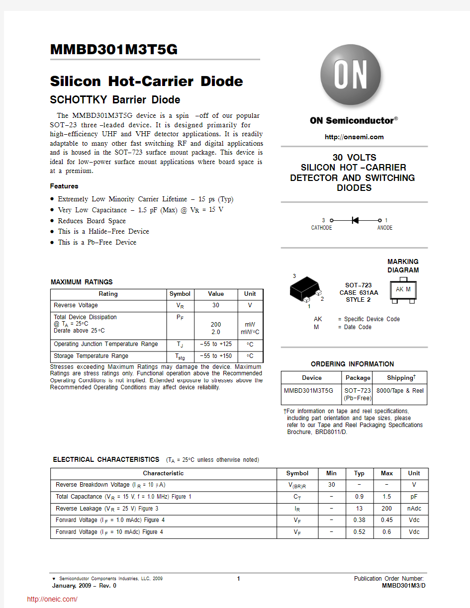
Silicon Hot-Carrier Diode
SCHOTTKY Barrier Diode
The MMBD301M3T5G device is a spin ?off of our popular SOT ?23 three ?leaded device. It is designed primarily for high ?efficiency UHF and VHF detector applications. It is readily adaptable to many other fast switching RF and digital applications and is housed in the SOT ?723 surface mount package. This device is ideal for low ?power surface mount applications where board space is at a premium.
Features
?Extremely Low Minority Carrier Lifetime ? 15 ps (Typ)?V ery Low Capacitance ? 1.5 pF (Max) @ V R = 15 V ?Reduces Board Space
?This is a Halide ?Free Device ?
This is a Pb ?Free Device
MAXIMUM RATINGS
Rating
Symbol Value Unit Reverse Voltage V R 30V T otal Device Dissipation @ T A = 25°C
Derate above 25°C
P F
2002.0mW mW/°C Operating Junction T emperature Range T J ?55 to +125°C Storage T emperature Range
T stg
?55 to +150
°C
Stresses exceeding Maximum Ratings may damage the device. Maximum Ratings are stress ratings only. Functional operation above the Recommended Operating Conditions is not implied. Extended exposure to stresses above the Recommended Operating Conditions may affect device reliability.
ELECTRICAL CHARACTERISTICS (T A = 25°C unless otherwise noted)
Characteristic
Symbol Min Typ Max Unit Reverse Breakdown Voltage (I R = 10 m A)
V (BR)R 30??V T otal Capacitance (V R = 15 V, f = 1.0 MHz) Figure 1C T ?
0.9 1.5pF Reverse Leakage (V R = 25 V) Figure 3I R ?13
200nAdc Forward Voltage (I F = 1.0 mAdc) Figure 4V F ?0.380.45Vdc Forward Voltage (I F = 10 mAdc) Figure 4
V F
?
0.52
0.6
Vdc
https://www.360docs.net/doc/2416338246.html,
30 VOLTS
SILICON HOT ?CARRIER DETECTOR AND SWITCHING
DIODES
Device Package
Shipping ?
ORDERING INFORMATION
MMBD301M3T5G
SOT ?723(Pb ?Free)
8000/T ape & Reel ?For information on tape and reel specifications,including part orientation and tape sizes, please refer to our T ape and Reel Packaging Specifications Brochure, BRD8011/D.
SOT ?723CASE 631AA STYLE 2
AK M
AK = Specific Device Code M = Date Code
MARKING DIAGRAM
13
https://www.360docs.net/doc/2416338246.html,
2
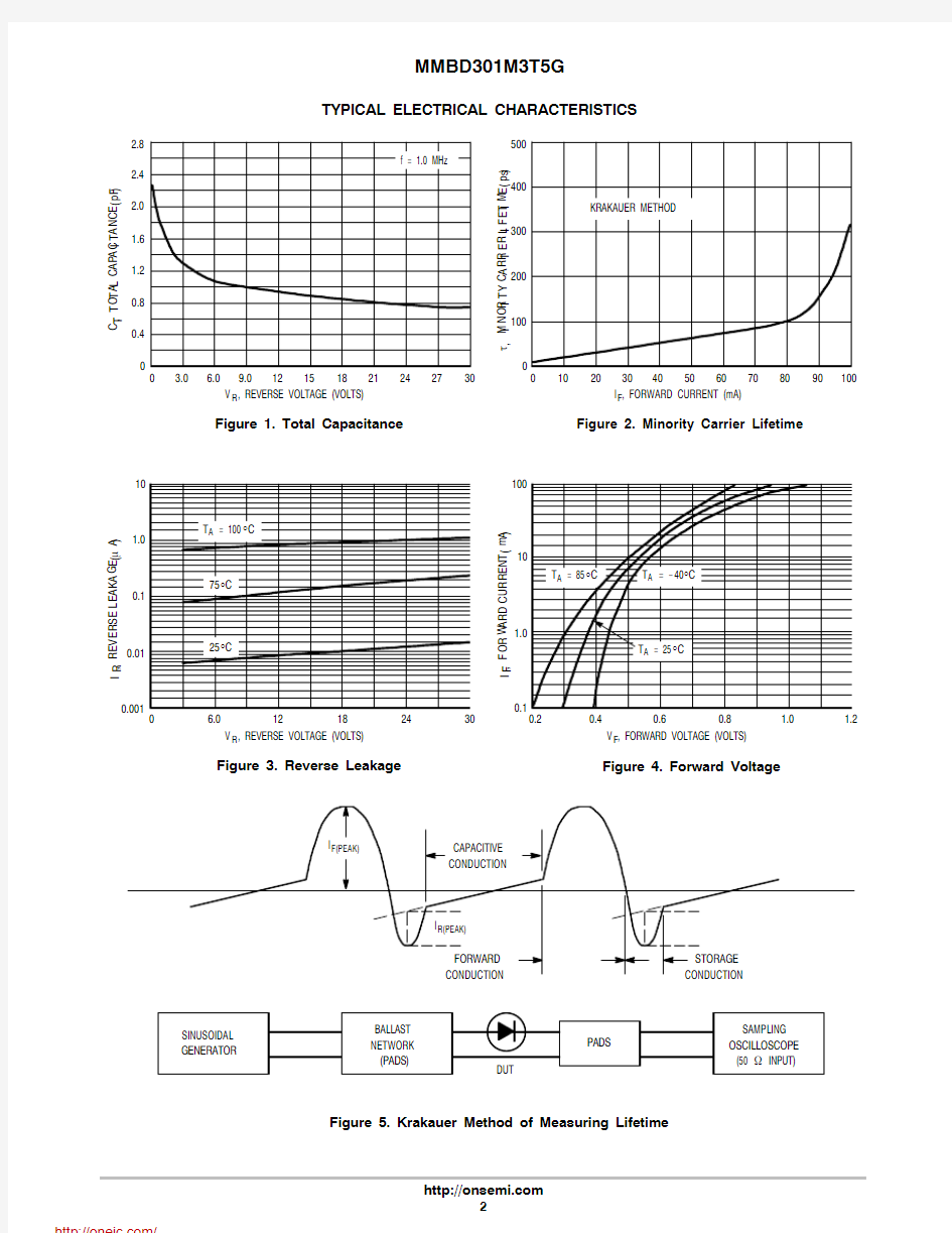
TYPICAL ELECTRICAL CHARACTERISTICS
Figure 1. Total Capacitance V R , REVERSE VOLTAGE (VOLTS)
Figure 2. Minority Carrier Lifetime
I F , FORWARD CURRENT (mA)
Figure 3. Reverse Leakage V R , REVERSE VOLTAGE (VOLTS)
Figure 4. Forward Voltage
V F , FORWARD VOLTAGE (VOLTS)
, F O R W A R D C U R R E N T (m A )
I F , R E V E R S E L E A K A G E ( A )
I R m 0.20.4
0.60.8
1.0 1.2
0 6.0
1218
24
01020
3.0
6.0
9.0121521
1.630
24
27
181.20.80.4304050607080100
9002.82.42.030
, T O T A L C A P A
C I T A N C E (p F )
C T , M I N O R I T Y C A R R I E R L I F E T I M E
(p s )
t Figure 5. Krakauer Method of Measuring Lifetime
PACKAGE DIMENSIONS
STYLE 2:
PIN 1.ANODE 2.N/C
3.CATHODE
SOT ?723CASE 631AA ?01
ISSUE C
DIM MIN NOM MAX MILLIMETERS A 0.450.500.55b 0.150.210.27b10.250.310.37C 0.070.120.17D 1.15 1.20 1.25E 0.750.800.85
e 0.40 BSC
H 1.15 1.20 1.25L
0.150.200.250.0180.0200.0220.00590.00830.01060.0100.0120.0150.00280.00470.00670.0450.0470.0490.030.0320.034
0.016 BSC
0.0450.0470.0490.00590.00790.0098
MIN NOM MAX INCHES
E NOTES:
1.DIMENSIONING AND TOLERANCING PER ANSI Y14.5M, 198
2.
2.CONTROLLING DIMENSION: MILLIMETERS.
3.MAXIMUM LEAD THICKNESS INCLUDES LEAD
FINISH. MINIMUM LEAD THICKNESS IS THE MINIMUM THICKNESS OF BASE MATERIAL.
4.DIMENSIONS D AND E DO NOT INCLUDE MOLD FLASH, PROTRUSIONS OR GATE BURRS.
ǒmm inches
ǔSCALE 20:1
*For additional information on our Pb ?Free strategy and soldering
details, please download the ON Semiconductor Soldering and Mounting T echniques Reference Manual, SOLDERRM/D.
SOLDERING FOOTPRINT*
ON Semiconductor and are registered trademarks of Semiconductor Components Industries, LLC (SCILLC). SCILLC reserves the right to make changes without further notice to any products herein. SCILLC makes no warranty, representation or guarantee regarding the suitability of its products for any particular purpose, nor does SCILLC assume any liability arising out of the application or use of any product or circuit, and specifically disclaims any and all liability, including without limitation special, consequential or incidental damages. “Typical” parameters which may be provided in SCILLC data sheets and/or specifications can and do vary in different applications and actual performance may vary over time. All operating parameters, including “Typicals” must be validated for each customer application by customer’s technical experts. SCILLC does not convey any license under its patent rights nor the rights of others. SCILLC products are not designed, intended, or authorized for use as components in systems intended for surgical implant into the body,or other applications intended to support or sustain life, or for any other application in which the failure of the SCILLC product could create a situation where personal injury or death may occur. Should Buyer purchase or use SCILLC products for any such unintended or unauthorized application, Buyer shall indemnify and hold SCILLC and its officers, employees,subsidiaries, affiliates, and distributors harmless against all claims, costs, damages, and expenses, and reasonable attorney fees arising out of, directly or indirectly, any claim of personal injury or death associated with such unintended or unauthorized use, even if such claim alleges that SCILLC was negligent regarding the design or manufacture of the part.SCILLC is an Equal Opportunity/Affirmative Action Employer. This literature is subject to all applicable copyright laws and is not for resale in any manner.
PUBLICATION ORDERING INFORMATION
分销商库存信息: ONSEMI
MMBD301M3T5G