SOC_design&Test6

System-on-a-Chip Design and Test:
Part 1 -Methods
Lecture 6
Design for testability
Nicola Nicolici
Computer-Aided Design and Test Research Group
McMaster University
该文由浅入深的讲解了SOC设计和测试的基本方法。全文共分9部分, 该文版权归作者与McMaster University版权所有。
由https://www.360docs.net/doc/3c1343333.html,和https://www.360docs.net/doc/3c1343333.html,收集整理,仅供本站内部学习讨论。
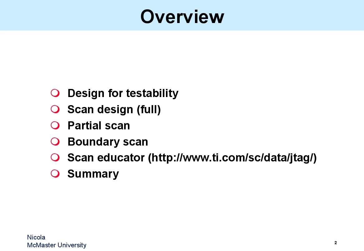
Overview
Design for testability
Scan design (full)
Partial scan
Boundary scan
Scan educator (https://www.360docs.net/doc/3c1343333.html,/sc/data/jtag/) Summary
Design for testability
Design for testability(DFT): design techniques that make test generation and test application cost-effective
Design practices learnt through experience as guidelines:?Avoid asynchronous (unclocked) feedback
?Make flip-flops initializable
?Avoid redundant gates and avoid large fanin gates
?Provide test control for difficult-to-control signals
?Avoid gated clocks
Disadvantages of ad-hoc DFT methods:
?Experts and tools not always available
?Tests with no guarantee of high fault coverage
?Design iterations may be necessary
Scan design
Circuit is designed using pre-specified design rules
Test structure is added to the verified design:
?Add a test control(TC) primary input
?Replace flip-flops by scan flip-flops(SFF)
?Connect SFF to form one or more shift registers
?Scan input controlled through primary inputs (PI)
?Scan output observed through primary outputs (PO) Use combinational test generation to obtain tests!
Add shift register tests for use in manufacturing test
Scan design rules
Use only clocked D-type of flip-flops for all state variables At least one PI pin must be available for test:
?More pins, if available, can be used
All clocks must be controlled from PIs
Clocks must not feed data inputs of flip-flops
Correcting a rule violation All clocks must be controlled from PIs.
Comb.
logic D1
D2
Comb.
logic
Q
FF
Comb.
logic
D1
D2
CK
Q
FF
Comb.
logic
Scan flip flop
MUX
Logic overhead
D flip-flop
Master latch Slave latch
D TC
Q
Q
SD
CK
Slave open
Master open
CK
t
Normal mode, D selected
Scan mode, SD selected
TC
t
Adding scan structure
Combinational
logic SFF SFF SFF
PI PO
SCANOUT TC or TCK Not shown: CK or
MCK/SCK feed all
SFFs.
SCANIN
Testing combinational logic
I2
I1
S1 S2
Don’t care or random
bits
PI
SCANIN
TC
0 0 0 0 0 0 0 1 0 0 0 0 0 0 0 1 0 0 0 0 0 0 0
O1O2
N1 N2
PO
SCANOUT
n comb = number of combinational vectors n sff = number of scan flip-flops
Testing sequential logic
Scan register tested before of combinational logic
A shift sequence 00110011 . . . of length n sff+4in scan
mode (TC=0) produces 00, 01, 11 and 10 transitions in all flip-flops and observes the result at SCANOUT output
Total scan test length: (n comb+ 2)n sff+n comb+ 4 clocks 2,000 scan flip-flops, 500 combinational vectors:?Total scan test length ~ 106clocks
Multiple scan registers reduce test length
Multiple scan chains
Scan flip-flops can be distributed among any number of
shift registers, with separate scanin and scanout pins Test sequence length given by the longest scan chain Just one test control (TC) pin is essential
PI
PO
Combinational
logic
SFF
SFF
SFF
CK
TC Scan Out
Scan overhead
Input/Output pins:
?At least one pin necessary (TC)
?Scan in and scan out pins if not multiplexed with PI/PO Area overhead:
?Gate overhead = [4n sff /(n g +10n ff )] x 100%, where n g = comb. gates ;n ff = flip-flops ; Example –n g = 100k gates ,n ff = 2k flip-flops , overhead = 6.7%
?Accurate estimate considers wiring and layout area Performance overhead:
?Multiplexer delay added in combinational path:
–Approximate two gate-delays
?Flip-flop output loading due to one additional fanout:
–Approximate 5-6%
Hierarchical scan
Scan flip-flops are chained within subnetworks: Advantages:
?Automatic scan insertion in netlist ?Circuit hierarchy preserved
?Helps in debugging and design changes Disadvantage: Non-optimum chip layout
SFF3
SFF1
SFF2
SFF4SFF1
SFF2
SFF3
SFF4
Scanout
Scanin
Scanin
Hierarchical netlist
Flat layout
Optimum scan layout
Interconnects
Routing channels
IO pad Flip-flop cell
SFF cell
TC
X’
X
Y’Y
Active areas: XY and X’Y’
Linear dimensions of active area:
X = (C + S) / r
X’ = (C + S +aS) / r
Y’ = Y + ry = Y + Y(1--b) / T
Area overhead:
X’Y’--XY
= --------------x 100%
XY
1--b
= [(1+as)(1+ -------)–1]x 100%
T
1--b
= (as + -------)x 100%
T y = track dimension, wire width+separation C = total comb. cell width
S = total non-scan FF cell width
s = fractional FF cell area = S/(C+S)
a = SFF cell width fractional increase
r = number of cell rows or routing channels b = routing fraction in active area
T = cell height in track dimension y
2,000-gate CMOS chip
Fractional area under flip-flop cells, s = 0.478 Scan flip-flop (SFF) cell width increase, α = 0.25 Routing area fraction, β = 0.471
Cell height in routing tracks, T = 10
Calculated overhead = 17.24%
Actual measured data:
Scan implementation Area overhead Normalized clock rate
_________________________________________________________ None 0.0 1.00
Hierarchical 16.93% 0.87
Optimum layout 11.90% 0.91
Scan test generation benefits
Reduce sequential automatic test pattern generation (ATPG) to combinational ATPG
Original
2,781
179
0.0%
4,603
35/49
70.0%
70.9%
5,533 s
414
414
Full-scan
2,781
179
15.66%
4,603
214/228
99.1%
100.0%
5 s
585
105,662
Number of combinational gates
Number of non-scan flip-flops (10 gates each)
Number of scan flip-flops (14 gates each)
Gate overhead
Number of faults
PI/PO for ATPG
Fault coverage
Fault efficiency
CPU time on SUN Ultra II, 200MHz processor
Number of ATPG vectors
Scan sequence length
Scan automation
Behavior, RTL, and logic
Design and verification
Rule
violations
Scan design
rule audits
Gate-level
netlist
Combinational
ATPG
Scan hardware
insertion
Chip layout: Scan-
chain optimization,
timing verification Scan sequence
and test program
generation
Scan chain order
Combinational
vectors
Scan
netlist
Design and test
data for
manufacturing Mask data
Test program
Timing and power issues
Scan delays and clock skew can cause race condition Large delays in scan path require slower scan clock
Random signal activity in combinational circuit during scan can cause excessive power dissipation
Need for new solutions:
?Maintain the benefit of combinational ATPG
?Reduce the overhead
Partial scan!
Partial scan
A subset of flip-flops is scanned
Objectives:
?Minimize area overhead and scan sequence length ?Achieve required fault coverage
?Exclude selected flip-flops from scan:
–Improve performance
–Allow limited scan design rule violations ?Allow automation:
–In scan flip-flop selection
–In test generation
?Shorter scan sequences