电磁兼容论文1
Estimating Radio-Frequency Interference to an
Antenna Due to Near-Field Coupling Using
Decomposition Method Based on Reciprocity Hanfeng Wang,Student Member,IEEE,Victor Khilkevich,Member,IEEE,Yao-Jiang Zhang,Senior Member,IEEE,
and Jun Fan,Senior Member,IEEE
Abstract—In mixed radio-frequency(RF)and digital designs, noise from high-speed digital circuits can interfere with RF re-ceivers,resulting in RF interference issues such as receiver desen-sitization.In this paper,an effective methodology is proposed to estimate the RF interference received by an antenna due to near-?eld coupling,which is one of the common noise-coupling mecha-nisms,using decomposition method based on reciprocity.In other words,the noise-coupling problem is divided into two steps.In the ?rst step,the coupling from the noise source to a Huygens surface that encloses the antenna is studied,with the actual antenna struc-ture removed,and the induced tangential electromagnetic?elds due to the noise source on this surface are obtained.In the second step,the antenna itself with the same Huygens surface is studied. The antenna is treated as a transmitting one and the induced tan-gential electromagnetic?elds on the surface are obtained.Then, the reciprocity theory is used and the noise power coupled to the antenna port in the original problem is estimated based on the results obtained in the two steps.The proposed methodology is val-idated through comparisons with full-wave simulations.It?ts well with engineering practice,and is particularly suitable for prelayout wireless system design and planning.
Index Terms—Decomposition,mixed radio-frequency(RF)/ digital design,near-?eld coupling to antenna,prelayout system design and planning,reciprocity,RF interference.
I.I NTRODUCTION
A S a special type of intrasystem electromagnetic compati-
bility(EMC)problem,radio-frequency(RF)interference from digital circuits to RF receivers is becoming increasingly critical in the design of mixed RF/digital systems[1].This is due to the increasing speed in digital integrated circuits(ICs)and the decreasing form factor of the systems.There are many pos-sible mechanisms for digital noise to couple to RF receivers.RF antennas/receivers can pick up digital noise through direct?eld coupling inside a metal chassis,such as from high-speed printed circuit board(PCB)traces,connectors,?ex cables,and IC heat sinks.Digital noise can also couple to RF antennas/receivers
Manuscript received August29,2012;revised November29,2012;accepted January10,2013.Date of publication March8,2013;date of current version December10,2013.This work was supported in part by the National Science Foundation(NSF)under Grant0855878.
The authors are with the EMC Laboratory,Missouri University of Science and Technology,Rolla,MO65409USA(e-mail:jfan@https://www.360docs.net/doc/392342119.html,).
Color versions of one or more of the?gures in this paper are available online at https://www.360docs.net/doc/392342119.html,.
Digital Object Identi?er
10.1109/TEMC.2013.2248090
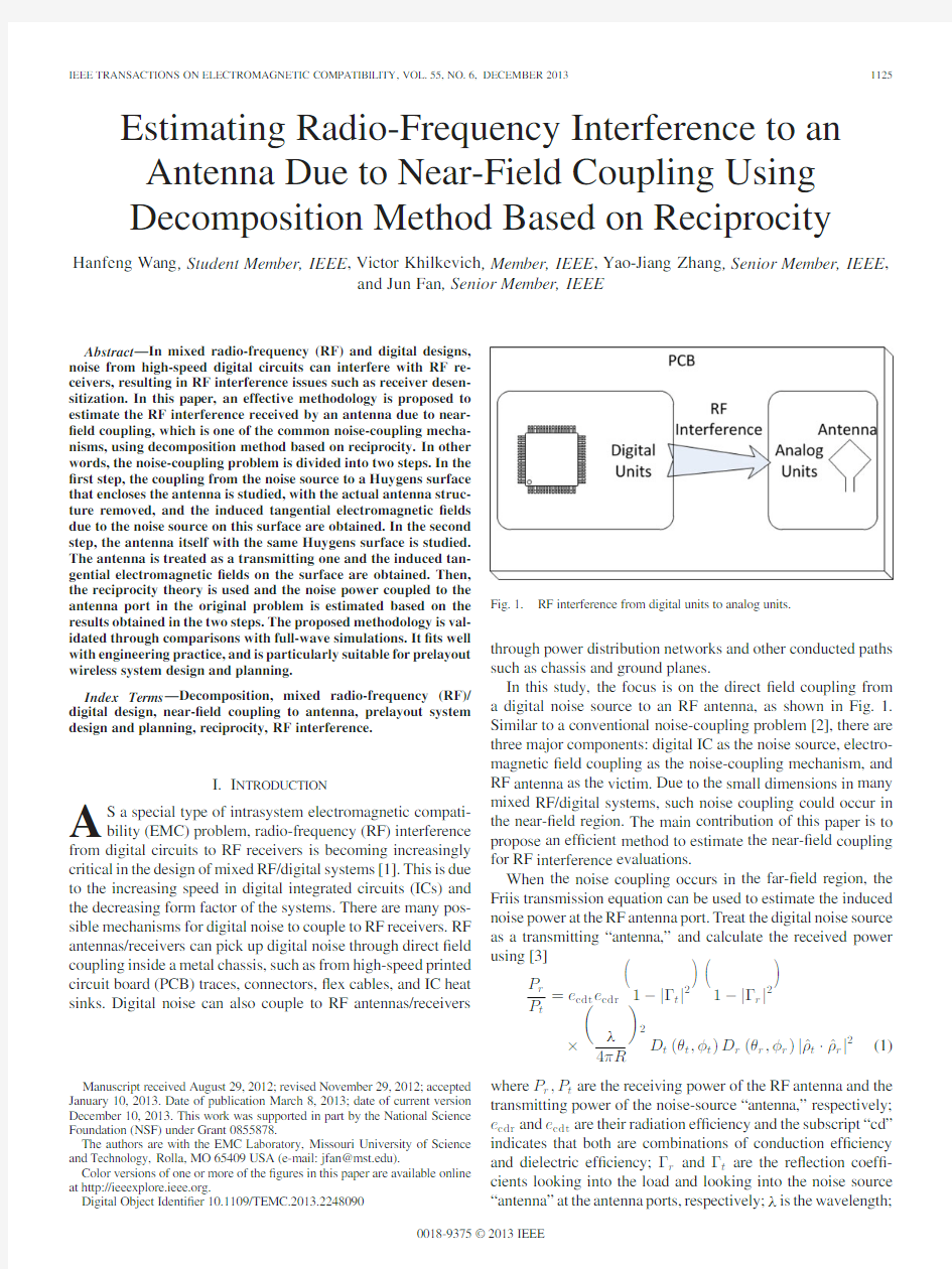
Fig.1.RF interference from digital units to analog units.
through power distribution networks and other conducted paths
such as chassis and ground planes.
In this study,the focus is on the direct?eld coupling from
a digital noise source to an RF antenna,as shown in Fig.1.
Similar to a conventional noise-coupling problem[2],there are
three major components:digital IC as the noise source,electro-
magnetic?eld coupling as the noise-coupling mechanism,and
RF antenna as the victim.Due to the small dimensions in many
mixed RF/digital systems,such noise coupling could occur in
the near-?eld region.The main contribution of this paper is to
propose an ef?cient method to estimate the near-?eld coupling
for RF interference evaluations.
When the noise coupling occurs in the far-?eld region,the
Friis transmission equation can be used to estimate the induced
noise power at the RF antenna port.Treat the digital noise source
as a transmitting“antenna,”and calculate the received power
using[3]
P r
P t
=e cdt e cdr
1?|Γt|2
1?|Γr|2
×
λ
4πR
2
D t(θt,φt)D r(θr,φr)|?ρt·?ρr|2(1)
where P r,P t are the receiving power of the RF antenna and the
transmitting power of the noise-source“antenna,”respectively;
e cdr and e cdt are their radiation ef?ciency and the subscript“cd”
indicates that both are combinations of conduction ef?ciency
and dielectric ef?ciency;Γr andΓt are the re?ection coef?-
cients looking into the load and looking into the noise source
“antenna”at the antenna ports,respectively;λis the wavelength; 0018-9375?2013IEEE
R is the distance between the two antennas;D r and D t are the
directivity of the two antennas;?ρr and ?ρ
t are the polarization unit vectors of the two antennas.The Friis transmission equation is a straightforward way to evaluate the receiving power (noise power in this case)at the RF antenna port.However,it only works for far-?eld coupling.It assumes 1/R distance depen-dence for the ?eld strength;however,in the near ?eld,there are 1/R 2and 1/R 3terms.Further,the Friis transmission equation is based on the plane-wave receiving properties of each antenna,which are built into the directivities.In the near-?eld case,the ?eld strength can vary strongly over the dimensions of the an-tenna and the plane wave behavior is not expected.In compact mobile devices,the coupling between the IC noise source and the RF antenna is mostly in the near-?eld region.Thus,the Friis transmission equation is no more suitable for this kind of prob-lems,which will be demonstrated using numerical simulations in Section IV .
Then,to estimate the noise power coupled to the RF antenna port from the digital circuit in near-?eld region,full-wave sim-ulation of the entire structure including the noise source,the RF receiving antenna,and all the relevant scatterers/materials is the straightforward,brute-force solution.However,this approach is time consuming for practical applications such as the prelayout system design and optimization in terms of the minimized RF interference,since full-wave model needs to be built and run for each con?guration.A more practical strategy is to generate “libraries”for digital noise source (IC)and antenna models,where interference estimation between the noise source and an-tenna models in a speci?c mechanical design can be ef?ciently obtained without the need to run lengthy full-wave simulations whenever a model,its location,or a mechanical feature changes.In this paper,a decomposition method based on reciprocity is introduced for estimating the received digital noise power at the RF antenna port,which ?ts very well with the engineering practice described earlier.First,a Huygens box is introduced to enclose the RF antenna so that it can be removed from the original structure.Then,the tangential electromagnetic ?elds on the Huygens box for the original structure with the RF antenna removed are obtained through a full-wave simulation (the noise source model obtained in [4]or similar ones can be used as the excitation).Next,the RF antenna alone is simulated as a transmitting antenna and the tangential electromagnetic ?elds on the same Huygens box are obtained.In other words,an antenna model is https://www.360docs.net/doc/392342119.html,stly,the induced noise power at the RF antenna port is obtained by using the two sets of the tangential electromagnetic ?elds on the Huygens box based on the reciprocity theorem.The bene?t of the proposed method is that the noise source and the antenna models remain the same as long as the same digital ICs and the same RF antenna are used.When component position changes or other mechanical design changes,only the electromagnetic ?elds on the Huygens box due to the noise source need to be recalculated,which is more ef?cient and faster than the full-wave simulation of the entire structure.Similarly,if several antenna designs are to be evaluated and compared,only individual antenna models need to be constructed (all other steps only need to be run once).This makes the prelayout design and optimization more ?exible and
ef?cient.
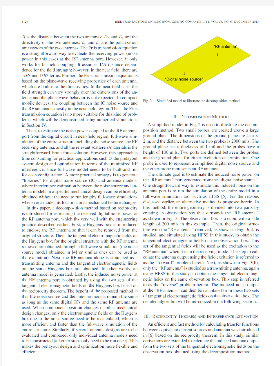
Fig.2.Simpli?ed model to illustrate the decomposition method.
II.D ECOMPOSITION M ETHOD
A simpli?ed model in Fig.2is used to illustrate the decom-position method.Two small probes are created above a large ground plane.The dimensions of the ground plane are 4in ×2in,and the distance between the two probes is 2000mils.The ground plane has a thickness of 1mil and the probes have a height of 100mils.Two ports are de?ned between the probes and the ground plane for either excitation or termination.One probe is used to represent a simpli?ed digital noise source and the other probe represents an RF antenna.
The ultimate goal is to estimate the induced noise power on the “RF antenna”port generated from the “digital noise source.”One straightforward way to estimate this induced noise on the antenna port is to run the simulation of the entire model in a full-wave simulation tool such as HFSS [5].For the reasons discussed earlier,an alternative method is proposed herein.In this method,the entire geometry is divided into two parts by creating an observation box that surrounds the “RF antenna,”as shown in Fig.3.The observation box is a cubic with a side length of 200mils in this example.Then,the original struc-ture with the “RF antenna”removed,as shown in Fig.3(a),is studied,and simulated using HFSS in this study,to obtain the tangential electromagnetic ?elds on the observation box.This set of the tangential ?elds will be used as the excitation to the “RF antenna”when it is in the receiving mode.The step to cal-culate the antenna output using the ?eld excitation is referred to as the “forward”problem herein.Next,as shown in Fig.3(b),only the “RF antenna”is studied as a transmitting antenna,again using HFSS in this study,to obtain the tangential electromag-netic ?elds on the same observation box.This step is referred to as the “reverse”problem herein.The induced noise output at the “RF antenna”can then be calculated from these two sets of tangential electromagnetic ?elds on the observation box.The detailed algorithm will be introduced in the following section.III.R ECIPROCITY T HEOREM AND I NTERFERENCE E STIMATION An ef?cient and fast method for calculating transfer functions between equivalent current sources and antenna was introduced in [6]based on the reciprocity theorem.In this study,similar derivations are extended to calculate the induced antenna output from the two sets of the tangential electromagnetic ?elds on the observation box obtained using the decomposition method.
W ANG et al.:ESTIMATING RADIO-FREQUENCY INTERFERENCE TO AN ANTENNA DUE TO NEAR-FIELD COUPLING
1127
Fig.3.Divide the whole model into two parts.(a)Part1including“digital noise source”and coupling path.(b)Part2including“RF antenna”only. The reciprocity theorem can be expressed using the?eld and source quantities in the forward and reserve problems as[7]:
?
S
ˉ
E rev×ˉH fwd?ˉE fwd×ˉH rev
·ds =
V
ˉ
E rev×ˉJ fwd+ˉH fwd×ˉM rev
dv
?
V
ˉ
E fwd×ˉJ rev+ˉH rev×ˉM fwd
dv(2)
whereˉJ is the electric current source andˉM is the magnetic current source.The superscript denotes the problem type,“fwd”for the forward problem and“rev”for the reverse one.If the integral is evaluated over the entire space(which means the boundary surface S is at in?nity),the left side of(2)is zero. Thus,(2)can be simpli?ed as
V ˉ
E rev
c
·ˉJ fwd
c
?ˉH rev c·ˉM fwd
c
dv
=
V
ˉ
E fwd
a
·ˉJ rev a?ˉH fwd a·ˉM rev a
dv(3)
where the subscript denotes the location of the source and?eld quantities:“c”for cells on observation box and“a”for the RF antenna port.Therefore,in the reverse problem,sources at the
antenna port are de?ned asˉJ rev
a andˉM rev
a
,and the resulting
?elds on the observation box are de?ned asˉE rev
c andˉH rev
c
.In
the forward problem,equivalent sources on the observation box
are de?ned asˉJ fwd
c andˉM fwd
c
,and the resulting?elds on the
antenna port are de?ned asˉE fwd
a andˉH fwd
a
.
The electric term at the left-hand side of(3)can be derived as
V
ˉJ fwd
c
·ˉE rev c dv=
S c
ˉJ fwd
c
·ˉE rev c ds=
cells
ˉJ fwd
c
·ˉE rev c S cell
=
cells
?n×ˉH fwd
c
·ˉE rev c S cell(4)
where S c is the surface of the observation box.The volume
integral becomes a surface integral since the equivalent electric
current densities in(4)only reside on the surface of the obser-
vation box.If the surface of the box is meshed into uniform
square cells,and the meshed cells are small enough so that the
?elds are approximately uniform inside each cell,the integral
can be transformed into summations where S cell is the area of
each mesh cell.Finally,the equivalent electric current densities
on the surface of the observation box can be calculated from the
H-?eld,where n is the inward unit vector normal to the surface
of the observation box.
Similarly,the magnetic term at the left side of(3)can be
derived as
V
ˉM fwd
c
·ˉH rev c dv=
S c
ˉM fwd
c
·ˉH rev c ds
=
cells
ˉM fwd
c
·ˉH rev c S cell=
cells
ˉE fwd
c
×?n·ˉH rev c S cell.(5)
The electric term at the right-hand side of(3)can be derived
similarly as in[8]as
V
ˉE fwd
a
·ˉJ rev a dv=?
S a
E fwd
a
J rev
a
ds=?I rev
a
U fwd
a
(6)
where the volume integral is transformed into a surface integral
at the antenna port surface.The negative sign is becauseˉE fwd
a
andˉJ rev
a
have opposite directions.S a is the cross-sectional
surface of the antenna port.U fwd
a
and I rev
a
are the voltage and
current at the antenna port in the forward and reverse problems,
respectively.
The magnetic term at the right-hand side of(3)is?rst con-
verted to an electric term as
V
ˉH fwd
a
·ˉM rev a dv=
V
ˉ
E rev
a
×?n
·ˉH fwd a dv
=
V
ˉE rev
a
·
?n×ˉH fwd
a
dv=
V
ˉE rev
a
·ˉJ fwd
a
dv.(7)
Then,(7)can be similarly derived as in(6)as
V
ˉE rev
a
·ˉJ fwd
a
dv=
S a
J fwd
a
E rev
a
ds=I fwd
a
U rev
a
.(8)
Substituting(4)–(8)back into(3)results in
cells
ˉn×ˉH fwd
c
·ˉE rev c S cell+
cells
ˉn×ˉE fwd
c
·ˉH rev c S cell
=?I rev
a
U fwd
a
?I fwd a U rev a=?
1
Z in
+
1
Z L
U fwd
a
U rev
a
(9)
where Z in is the input impedance of the RF antenna in the trans-
mitting mode in the reverse problem,Z L the load impedance
at the antenna port in the receiving mode(50Ωin our case)in
the forward problem,and U rev
a
is the exciting voltage of the RF
1128IEEE TRANSACTIONS ON ELECTROMAGNETIC COMPATIBILITY ,VOL.55,NO.6,DECEMBER 2013
antenna in the transmitting mode (1V in our case).From (9),
the voltage induced at the RF antenna port U fwd
a
can be solved from the tangential E and H ?elds on the observation box in both the reverse and the forward problems as follows:
U fw d a =?
Z in Z L
U rev a (Z in +Z L
)×
cells
ˉn ×ˉH fw d c ·ˉE rev c S cell + cells
ˉn ×ˉE fw d c ·ˉH rev c S cell .(10)
It needs to be pointed out that the simple decomposition
method proposed in this study assumes that the multiple scat-tering effects between the noise source and the RF antenna are negligible.
IV .R ESULTS AND V ALIDATIONS
A.Simple Model
The simple probe model in Fig.2is ?rst used to prove the necessity of the study of near-?eld coupling.The Friis trans-mission equation [3]is used to estimate the induced power at the port of the receiving “RF antenna,”and it will be shown that this equation only works when the noise-source antenna and the “RF antenna”are located suf?ciently far away to each other.In this example,since both the noise-source and the “RF”antennas have the same probe structure.Their parameters,such as the directivity,the gain and the input impedance,can be obtained by simulating one probe antenna alone in HFSS.The peak gain of the probe antenna is 2.97and the input impedance is Z in =(3.719–161.5j)Ω.The peak gain is the multiplication of the peak directivity and the radiation ef?ciency.The re?ection coef?cient can be calculated as:
|Γ|=
Z in ?Z L Z in +Z L
(11)where Z in is the input impedance of the probe antenna and
Z L =50Ω,assuming both probes are either terminated with a 50Ωload or connected with a source with a 50Ωsource resistance.Since the two probe antennas are aligned in their maximum radiation direction and are also polarization-matched,the receiving power at the “RF antenna”can be easily calculated from (1).A sinusoidal wave of magnitude of 1V is assumed as the source voltage for the transmitting antenna in the results shown below.
Meanwhile,the power induced at the port of the receiving antenna can also be obtained from the full-wave simulation of the entire structure with both probes (denoted direct method)and from the proposed decomposition method using (10).The mesh size on the observation box,when using the proposed method,is 5mils,which was found to be suf?ciently small to obtain the converged results in this example.The results of the three methods are compared in Fig.4,with the distance between the two probes changing from 500to 2000mils.
It can be clearly seen that the difference between the Friis transmission equation and the full-wave simulation becomes larger when the distance between the two probes becomes smaller.This means that the Friis transmission equation
can
https://www.360docs.net/doc/392342119.html,parison of the Friis transmission equation,the direct full-wave simulation,and the proposed decomposition method at 10GHz.
only be used to estimate the receiving power for far-?eld cou-pling.However,for the RF interference problems in compact mobile devices,near-?eld coupling could be dominant.There-fore,the Friis transmission equation is no longer suitable in these cases.The results of the direct full-wave simulation and the proposed decomposition method show a strong agreement for all the cases.The frequency under study in this example is 10GHz.
Further,the same model in Fig.2,when the distance between the two probes is 500mils,is used to validate the proposed method at different frequencies.The induced power at the re-ceiving antenna port at each frequency point was calculated using (10)?rst,and then obtained from the full-wave simula-tion of the entire structure.The two sets of results are compared at ten different frequency points from 1to 10GHz in Fig.5.The difference between the proposed method and the direct full-wave simulation of the entire structure is within 0.06dB.With the decrease of frequency,the electrical distance between the two probes is reduced in terms of the wavelength and the er-ror using the Friis transmission equation increases signi?cantly,as clearly shown in Fig.5.At the frequencies above 8GHz,the difference between the Friis transmission equation and the other two methods increases again.This is possibly due to insuf?cient mesh size at these frequencies.Since the probe is very small,the simulated frequency range is out of the resonant frequency of the antenna.Thus,the coupled power to the antenna port is very small.Two more practical examples are used to validate the proposed method in the following sections.B.Trace +PIFA
A more practical case,with a section of microstrip trace and a planar inverted-F antenna (PIFA)[9],is shown in Fig.6.The ground plane size is 4in ×2in and the thickness of the plane is 1mil.The patch of the PIFA has dimensions of 500mils ×500mils and is 10mils above the ground plane.The radius of
W ANG et al.:ESTIMATING RADIO-FREQUENCY INTERFERENCE TO AN ANTENNA DUE TO NEAR-FIELD COUPLING
1129
Fig.5.Output power comparison among the Friis transmission equation,the proposed method,and the direct full-wave simulation for the simpli?ed model shown in Fig.
2.
Fig.6.Near-?eld coupling from a microstrip trace to a PIFA antenna.
the short via and feeding probe of the PIFA is 10mils,and the antipad radius of the feeding port is 30mils.The trace (digital noise source)is excited with a 1V voltage source with a 50Ωsource resistance at one end and terminated with a 50Ωat the other end.The detailed dimensions for the trace can be found in [4].The distance between the trace and the PIFA is 2000mils.This example represents a typical near-?eld coupling problem from a digital trace to an RF antenna in modern mobile devices.The proposed decomposition method is used to calculate the induced power at the PIFA port.An observation box with the dimensions of 1000mils ×1000mils ×200mils is created to enclose the PIFA antenna.The mesh size on the observation box is 10mils.The calculated power is validated through the com-parisons with the full-wave simulation of the entire structure,as shown in Fig.7.
The agreement between the two methods is excellent in gen-eral in the entire frequency range from 3.1to 5.1GHz,with some small discrepancies close to 4.1GHz,the resonant frequency of the PIFA
antenna.
Fig.7.Output power comparisons between the proposed method and the direct method for the trace +PIFA structure shown in Fig.6.
There are several factors that may in?uence the accuracy of the proposed decomposition method.Based on the derivation of the reciprocity theorem,the observation box only needs to be big enough to enclose the RF antenna.Numerical experiments have also validated this conclusion.The distance between the noise source and the antenna is varied,and results have shown excellent agreement of the proposed method compared with the full-wave simulation of the entire structure,even for the very closely coupled cases as long as the noise source does not in?uence the radiation pattern of the antenna and the multiple scattering effects between the noise source and the antenna can be neglected.The mesh size on the observation box has been found very critical for the proposed method.Since the integral is approximated using the summation,the tangential components of the ?elds need to be approximately constant in each mesh cell.Thus,the size of the mesh cell is determined by both the wavelength and the variation of the ?elds on the observation box.The mesh cell size needs to be smaller than 1/10th of the wavelength.Furthermore,if the box is at the very near ?eld of the antenna (meaning the ?eld is changing dramatically on the surface of the box),the mesh cell size needs to be further smaller.C.DECT +IC
The last example to validate the proposed method is extracted from a real product [10].The near-?eld coupling between a Dig-ital Enhanced Cordless Telecommunications (DECT)antenna and an IC is studied as shown in Fig.8.The DECT antenna is on the edge of a printed circuit board,and one I/O port of the IC is excited as the noise source.The detailed dimensions of the DECT antenna are shown in Fig.9,and the thickness of the antenna is 0.709mils.The distance between the centers of the IC to the DECT antenna is 1949mils.The size of the die of the IC is 141.7mils ×433.1mils,and it has 27×2pins.The detailed modeling information of the IC is described in [10].
1130IEEE TRANSACTIONS ON ELECTROMAGNETIC COMPATIBILITY ,VOL.55,NO.6,DECEMBER
2013
Fig.8.Near-?eld coupling from an IC to a DECT antenna on a real printed circuit
board.
Fig.9.Detailed dimensions of the DECT antenna (the values outside the parentheses are in millimeters and the values inside the parentheses are in
mil).
Fig.10.Output power comparisons between the proposed method and the
direct method for the DECT +IC structure shown in Fig.8.
The induced power on the DECT antenna port is evaluated us-ing both the proposed decomposition method and the full-wave simulation method of the entire structure.The dimensions of the observation box enclosing the DECT antenna are 551.1mils ×1732mils ×551.1mils,and the mesh size on the observation box is 39.37mils.The results are compared in Fig.10.
The resonant frequency of the DECT antenna is 1840MHz.The results of the output power at the antenna port from the two methods from 1340to 2340MHz with a 100MHz
step
Fig.11.
PIFA antenna rotated by 90?from Fig.
6.
Fig.12.Output power comparisons between the proposed method and the direct method for the trace +PIFA structure shown in Fig.11.
are compared in Fig.10.The difference between the proposed method and the direct full-wave simulation is within 0.8dB,which demonstrates that the proposed method is valid even when the antenna is at the edge of the board.D.Application in Prelayout Design
The proposed decomposition method breaks the modeling of the entire interference problem into two separate simulations.The main advantage of the proposed method is its application in prelayout planning and design.At this early design stage,both the antenna type and the component placement need to be determined.To achieve optimal performance in terms of the minimized RF interference,different antennas and/or different IC/antenna placements may need to be evaluated.If the direct full-wave method is used,multiple time-consuming simulations are needed whenever the antenna con?guration or the compo-nent placement changes.In other words,if K antenna con?gura-tions and L placement con?gurations are to be evaluated,totally K ×L full-wave simulations may have to be performed.How-ever,using the proposed decomposition method,only K +L full-wave simulations may be necessary.When K and L val-ues are larger,K +L < W ANG et al.:ESTIMATING RADIO-FREQUENCY INTERFERENCE TO AN ANTENNA DUE TO NEAR-FIELD COUPLING1131 method is much more ef?cient than the direct method in this kind of engineering applications. To demonstrate the idea,the PIFA and trace example in Fig.6 are revisited.The PIFA antenna is simply rotated by90?and the same Huygens box is used,as shown in Fig.11. In this example,no new simulations are necessary.The an-tenna model obtained in Section IV-B is simply rotated by90?through coordinate transformation,and then the noise power received at the antenna is estimated using the decomposition method.The result is compared with the direct full-wave simula-tion in Fig.12.Again,the difference is small,with the maximum value at the resonant frequency of the antenna less than3dB. V.C ONCLUSION A decomposition method is introduced for estimating the near-?eld noise coupling from a digital noise source to an RF antenna.The reciprocity theorem is used to obtain the antenna noise output based on the modeling of the forward and reserve problems.Three examples,from a simpli?ed model to a practi-cal model extracted from a real product,are used to validate the proposed method.The calculated results using the decomposi-tion method based on the reciprocity theorem show excellent agreement of the induced noise at the RF antenna port with the direct full-wave simulations of the original geometry.The proposed method?ts well with typical engineering practice and can be used for ef?cient prelayout design and optimization.The multiple scattering effects between the antenna and other scat-ters/sources in the system are neglected in this study. A CKNOWLEDGMENT The authors would like to thank H.Li with the Electromag-netic Compatibility Laboratory,Missouri University of Science and Technology,Rolla,MO,USA,for providing the DECT+IC HFSS model for the noise-coupling study in this paper. R EFERENCES [1]K.Slattery and H.Skinner,Platform Interference in Wireless Systems: Models,Measurement,and Mitigation.Burlington,MA,USA:Newnes, 2008. [2] C.R.Paul,Introduction to Electromagnetic Compatibility.Hoboken, NJ,USA:Wiley,2006. [3] C.A.Balanis,Antenna Theory:Analysis and Design,3rd ed.Hoboken, NJ,USA:Wiley,2005,pp.94–96. [4]Z.Yu,J.A.Mix,S.Sajuyigbe,K.P.Slattery,and J.Fan,“An improved dipole-moment model based on near-?eld scanning for characterizing near-?eld coupling and far-?eld radiation from an IC,”IEEE https://www.360docs.net/doc/392342119.html,pat.,vol.55,no.1,pp.97–108,2013. [5]HFSS.(2011).[Online].Available:https://www.360docs.net/doc/392342119.html,/staticassets/ ANSYS/staticassets/resourcelibrary/brochure/ansys-hfss-brochure-14.0. pdf [6]V.Khilkevich,“An ef?cient and fast method of calculating transfer func- tions between equivalent current sources and antennas,”to be published. [7] C.A.Balanis,Advanced Engineering Electromagnetics.Hoboken,NJ, USA:Wiley,1989,pp.323–325. [8]J.H.Richmond,“A reaction theorem and its applications to antenna impedance calculations,”IRE Trans.Antennas Propag.,vol.9,no.6, pp.515–520,Nov.1961. [9]K.-L.Wong,Planar Antennas for Wireless Communications.Hoboken, NJ,USA:Wiley,2003,pp.3–48. [10]H.Li,V.Khilkevich,D.Pommerenke,“Identi?cation and visualization of electromagnetic coupling path—Part II:Practical application,”to be published. Hanfeng Wang(S’09)received the B.S.and M.S. degrees in electronic engineering from Tsinghua Uni- versity,Beijing,China,in2005and2008,respec- tively.He is currently working toward the Ph.D. degree from the Electromagnetic Compatibility Lab- oratory,Missouri University of Science and Technol- ogy,Rolla,USA. In2008,he joined the Electromagnetic Compati- bility Laboratory,Missouri University of Science and Technology.His current research interests include signal integrity,power integrity,and advanced nu-merical modeling. Victor Khilkevich(M’08)received the Ph.D.de- gree in electrical engineering from Moscow Power Engineering Institute,Technical University,Moscow, Russia,in2001. He is currently a Research Associate Professor at the Missouri University of Science and Tech- nology,Rolla,USA.His current research interests include computational electrodynamics,automotive electromagnetic compatibility modeling,and high- frequency measurement techniques. Yao-Jiang Zhang(S’97–M’01–SM’11)received B.E.and M.E.degrees in electrical engineering from the University of Science and Technology of China, Hefei,China,in1991and1994,respectively,and the Ph.D.degree in physical electronics from Peking University,Peking,China,in1999. From1999to2001,he was a Postdoctoral Research Fellow at Tsinghua University,Beijing, China.From August2001to August2006,he was a Senior Research Engineer at the Institute of High Performance Computing(IHPC),Agency for Sci-ence,Technology and Research(A?STAR),Singapore.From September2006 to September2008,he was a Postdoctoral Research Fellow in the EMC Labora-tory,Missouri University of Science and Technology(M S&T,formerly known as the University of Missouri-Rolla).From September2008to April2010,he was a Research Scientist at IHPC.Since April2010,he has been a Research Associate Professor in the EMC Laboratory,M S&T.His current research in-terests include analytical and numerical methods in electromagnetics,and their applications in signal/power integrity and electromagnetic interference issues for high-speed electronic packages or printed circuit boards. Jun Fan(S’97–M’00–SM’06)received the B.S.and M.S.degrees in electrical engineering from Tsinghua University,Beijing,China,in1994and1997,respec- tively,and the Ph.D.degree in electrical engineering from the Missouri University of Science and Technol- ogy(formerly University of Missouri-Rolla),Rolla, USA,in2000. From2000to2007,he was a Consultant En- gineer with the NCR Corporation,San Diego,CA, USA.In July2007,he joined the Missouri Univer- sity of Science and Technology(formerly University of Missouri-Rolla),where he is currently an Associate Professor with the EMC Laboratory.His current research interests include signal integrity and electro-magnetic interference(EMI)designs in high-speed digital systems,dc power-bus modeling,intrasystem EMI and radio-frequency interference,printed circuit board noise reduction,differential signaling,and cable/connector designs. Dr.Fan was the Chair of the IEEE EMC Society TC-9Computational Elec-tromagnetics Committee from2006to2008and was a Distinguished Lecturer of the IEEE EMC Society in2007and2008.He is currently the Vice Chair of the Technical Advisory Committee of the IEEE EMC Society.He received the IEEE EMC Society Technical Achievement Award in August2009.He is cur-rently an Associate Editor of the IEEE T RANSACTIONS ON E LECTROMAGNETIC C OMPATIBILITY and EMC Magazine. 滨江学院 课程论文 (电磁兼容原理、技术及应用) 题目电磁兼容与电磁干扰 学生姓名孔建民 学号20082305903 院系滨江学院电子工程 专业电子信息工程 指导教师吴大中 二零一零年十二月二十五日 摘要:本文在介绍电磁兼容与电磁干扰的概念上论述电磁兼容与电磁干扰的关系,分析了电磁干扰产生的原因,利用电磁兼容在各种情况下的应用,从根本上帮助解决电磁干扰产生的危害。例举各种情况下电磁兼容的方法,分析了电磁兼容的设计目的,展望电磁兼容的未来发展! 关键字:电磁兼容电磁干扰 一、电磁兼容(EMC)和电磁干扰(EMI) (一)电磁兼容(electromagnetic compatibility;EMC)的定义 国际电工委员会标准(IEC)对电磁兼容的定义是:电磁兼容是设备的一种能力,系统或设备在所处的电磁环境中能正常工作,同时不对其他系统和设备造成干扰。 电磁兼容性包括两方面:电磁干扰(electromagnetic interference ;EMI)、电磁耐受(electromagnetic susceptibility; EMI)。EMI指的是电气产品本身通电后,因电磁感应效应所产生的电磁波对周围电子设备所造成的干扰影响;EMS则是指电气产品本身对外来电磁波的干扰防御能力。 其中EMI包括:CE(传导干扰),RE(辐射干扰),PT(干扰功率测试)等等。EMS包括:ESD(静电放电),RS(辐射耐受),EFT/B(快速脉冲耐受),surge(雷击),CS(传导耐受)等等。 电磁兼容是研究电磁干扰的问题。在任何系统中,要形成电磁干扰必须具备3个基本条件,即骚扰源,对骚扰敏感的接收单元,把能量从骚扰源耦合到接收单元的传输通道,称为电磁干扰三要素。 (二)电磁兼容(EMC)的设计目的 显然,EMC 设计的目的就是使所设计的电子设备或系统在预期的电磁环境中能够实现电磁兼容。换而言之,就是说设计的电子设备或系统必须能够满足EMC 标准规定的两方面的能力:1)能在预期的电磁环境中正常工作,无性能降低或故障;2)对该电磁环境不是一个污染源。 (三)近年来电磁兼容(EMC)领域的发展概况 近年来,世界各国特别是发达国家,对EMC十分重视,大力发展EMC技术,制定相关的检测认证标准。如美国FCC标准、欧盟的89/336/EEC法规、日本的电波取缔法等。欧盟规定自1996年起,凡是未通过EMC认证和检测的任何电子、电工产品均不能在欧盟市场上流通。美国联邦通讯委员会FCC也明文规定,任何人不得出售、出租未经EMC检测认证的电子、电工产品,否则企业法人将被监禁并不得赎出。日本、韩国、新加坡、南非、加拿大等许多国家均有自己的EMC法规。国际电工委员会(IEC)下属的专门委员会制定了一系列的有关EMC的技术标准文件。 由此可见,了解EMC、EMI,掌握相关知识对于我国的电子产业发展和与国际接轨具有重要的意义。 二、电磁干扰(EMI)的原理及改善电磁兼容性的措施 (一)E MI的产生原因 PCB电磁兼容设计论文 学校:华北电力大学 专业:电子 班级: 0902 姓名:经权 学号:200903020213 第一章电磁兼容的概念及其相关标准介绍 第一节电磁兼容的概念 1.电磁兼容定义(Electromagnetic Compatibility即EMC) 1.1.1 国军标(GJB72A-2002)中给出电磁兼容的定义是: 设备、分系统、系统在共同的电磁环境中能一起执行各自功能并且互相不会影响各自正常工作的共存状态。包括以下两个方面: a)设备、分系统、系统在预定的电磁环境中运行时,可按规定的安全裕度实现设计的工作性能、且不因电磁干扰而受损或产生不可接受的降级; b)设备、分系统、系统在预定的电磁环境中正常地工作且不会给环境(或其他设备)带来不可接受的电磁干扰。 安全裕度——敏感度门限与环境中的实际干扰影响下性能降级或不能完成规定任务的特性。 1.1.2 名词解释 电磁骚扰——任何可能引起装置、设备或系统性能低或对有生命或无生命物质产生损害作用的电磁现象。 注:电磁骚扰可能是电磁噪声、无用信号或传播媒介自身的变化。 电磁干扰(EMI)——电磁骚扰引起的设备、传输通道或系统性能的下降。又可解释为:任何可能中断、阻碍,甚至降低、限制无线电通信或其他电子设备性能的传导或辐射的电磁能量。 辐射干扰——任何源自部件、天线、电缆、互连线的电磁辐射,以电场、磁场形式(或兼而有之)存在,并导致性能降级的不希望有的电磁能量。 传导干扰——沿着导体传输的不希望有的电磁能量,通常用电压或电流来定义。 电磁脉冲(EMP)——核爆炸或雷电放电时,在核设施或周围介质中存在光子散射,由此产生的康普顿反冲电子和光电子所导致新的电磁辐射。由电磁脉冲所产生的电场、磁场可能会与电子或电子系统耦合产生破坏性的电压和电流浪涌。 浪涌——沿线路或电路传播的电流、电压或功率的瞬态波。其特征最先快速上 电磁兼容——屏蔽学习心得 本人通过对多篇有关电磁兼容方面的论文的仔细研读和有关知识的了解,发现收获颇多,于是得到些许心得体会如下: EMC(电磁兼容)是设备的一种能力,它要求设备在其电磁环境中能正常完成它的功能,又不至于因为环境干扰而影响其正常工作。产品的 EMC 性能直接关系到产品的工作稳定性、环境适应能力。EMC 设计是通信产品设计中不可缺少的重要组成部分。 EMC 设计中比较关键的一项就是有关设备的屏蔽设计。屏蔽能有效地抑制通过空间传播的电磁干扰。采用屏蔽的目的有两个:一是限制内部的辐射电磁能越过某一区域;二是防止外来的辐射进入某一区域,现有的屏蔽措施都是基于这两个目的而施行。 目前,屏蔽系统已经为越来越多的用户所认识,它在电磁兼容方面的良好性能也正在为越来越多的人所认可。屏蔽系统具有良好的电磁兼容性,可以提供安全、高速、稳定的信息传输通道。屏蔽系统拥有一套完整的屏蔽、接地体系,提供最完整、最全面的电缆、部件及端到端全屏蔽解决方案,以满足当今网络日益提升的需求。对于屏蔽系统而言,接地是至关重要的过程,只有正确有效地接地才能体现出屏蔽的优越性和价值。 一.屏蔽系统的应用 1.信息安全:提高信息传输的安全性保证敏感数据不外漏,是选择屏蔽系统最重要的一个原因。随着网络信息化的普及,信息安全的重要性已经越来越被广大用户所重视,防止信息泄露就成为一个至关重要的问题。 2.高速网络:相对于100M和1000M的网络来说高速网络由于编码更复杂等原因,对外界的干扰更加敏感,通讯更容易受到外界的干扰。对屏蔽系统而言,屏蔽层屏蔽的不仅仅是外界电磁干扰,线缆之间的干扰也同样被隔离,屏蔽布线系统对ANEXT产生的影响具有先天的技术优势,所以屏蔽系统相对高速的网络运行更加稳定可靠。 3.特殊的传输环境:特殊的安装环境需要对外界的电磁干扰加以防护,比如建筑物附近有电台、电视台等强射频源,或者在大型动力装置附近,或者是各种的工业环境。这些环境中均有明确存在的连续或间断工作的强电磁干扰。在布线系统实施之前,虽然这些干扰对网络运行的影响很难定量分析,但使用屏蔽系 电磁干扰与电磁兼容 课程论文 论文题目:PCB电磁兼容性技术 专业: 班级: 学号: 姓名: 年月 目录 一:电磁兼容性技术概述.......................................................................................................... - 1 - 二:PCB设计中的电磁兼容问题 ............................................................................................. - 1 - 2.1 PCB形成干扰的基本要素: .......................................................................................... - 1 - 2.2 PCB中存在的电磁干扰分类: ................................................................................... - 2 - 三:印制电路板电磁兼容设计原则.......................................................................................... - 3 - 3.1印制电路板的层数、尺寸选择原则............................................................................ - 3 - 3.2器件布局原则................................................................................................................ - 3 - 3.3地线与电源线的设计原则............................................................................................ - 3 - 四:信号线设计原则.................................................................................................................. - 4 - 五:PCB 电磁兼容性设计中的相关注意事项 ........................................................................ - 5 - 六:结束语.................................................................................................................................. - 5 - 参考文献:.................................................................................................................................. - 6 - 课程论文 电磁兼容原理与实验技术 学生姓名:袁晓强 学号:110503231 学院:机械电子 班级:装控112 摘要: 电磁兼容技术是解决电磁干扰相关问题的一门技术.电磁兼容设计的目的是解决电路之间的相互干扰,防止电子设备产生过强的电磁发射,防止电子设备对外界干扰过度敏感. 电磁兼容(EMC)是一个新概念,它是抗干扰概念的扩展和延伸。从最初的设法防止射频频段内的电磁噪声、电磁干扰,发展到防止和对抗各种电磁干扰。进一步在认识上产生了质的飞跃,把主动采取措施抑制电磁干扰贯穿于设备或系统的设计、生产和使用的整个过程中。这样才能保证电子、电气设备和系统实现电磁兼容性。本文从电磁兼容标准,内容,技术,设计目的及展望未来发展! 关键词:电磁兼容电磁干扰 电磁兼容技术是解决电磁干扰相关问题的一门技术.电磁兼容设计的目的是解决电路之间的相互干扰,防止电子设备产生过强的电磁发射,防止电子设备对外界干扰过度敏感.近年来,电磁兼容设计技术的重要性日益增加,这有两个方面的原因:第一,电子设备日益复杂,特别是模拟电路和数字电路混合的情况越来越多、电路的工作频率越来越高,这导致了电路之间的干扰更加严重,设计人员如果不了解有关的设计技术,会导致产品开发周期过长,甚至开发失败.第二,为了保证电子设备稳定可靠的工作,减小电磁污染,越来越多的国家开始强制执行电磁兼容标准,特别是在美国和欧洲国家,电磁兼容指标已经成为法制性的指标,是电子产品厂商必须通过的指标之一,设计人员如果在设计中不考虑有关的问题,产品最终将不能通过电磁兼容试验,无法走上市场. 因此近年来,电磁兼容教育也在迅速发展,一方面,各种有关电磁兼容设计的书籍层出不穷,各种电子设计的期刊上也不断刊登有关的文章,另一方面,电磁兼容培训越来越受到欢迎.20世纪90年代末,美国参加电磁兼容培训的费用平均为每人每天330美元,目前,已经达到450美元左右,并且企业如果需要专场培训,往往需要与提供培训的公司提前半年签订合同,由此可以看到电子设计人员对电磁兼容技术的需求日益增加. 我国电磁兼容技术起步很晚,无论是理论、技术水平,还是配套产品(屏蔽材料、干扰滤波器等)制造,都与发达国家相差甚远.而与此形成强烈反差的是,在我们加入WTO以后,我们面对的是公平的国际竞争,各国之间唯一的贸易壁垒就是技术壁垒.而电磁兼容指标往往又是众多技术壁垒中最难突破的一道.因此,怎样使设计人员在较短的时间内,掌握电磁兼容设计技术,能够充满信心地面对挑战是 xxxx大学硕士生课程论文 电磁兼容与结构设计 电磁兼容概述 (2014—2015学年上学期) 姓名: 学号: 所在单位: 专业: 摘要 随着用电设备的增加,空间电磁能量逐年增加,人类生存环境具有浓厚的电磁环境内涵。在这种复杂的电磁环境中,如何减少相互间的电磁干扰,使各种设备正常运转,是一个亟待解决的问题;另外,恶略的电磁环境还会对人类及生态产生不良影响。电磁兼容正是为解决这类问题而迅速发展起来的学科。可以说电磁兼容是人类社会文明发展产生的无法避免的“副产品”。 电磁兼容一般指电气及电子设备在共同的电磁环境中能执行各自功能的共存状态,即要求在同一电磁环境中的上述各种设备都能正常工作,又互不干扰,达到兼容状态。电磁兼容技术是一门迅速发展的交叉学科,其理论基础涉及数学、电磁场理论、电路基础、信号分析等学科与技术,其应用范围几乎涉及到所有用电领域。 关键字:电磁兼容、电磁发射、传导耦合、辐射耦合、静电放电 1 引言 信息技术已经成为这个时代的主题,而信息时代的最突出特征,就是将电磁作为记录和传递信息的主要载体,人们对于电磁的利用无处不在。电磁日益渗入到金融、通信、电力、广播电视等事关国家安全的各个重要领域和社会生活的各个角落,电磁已经成为了信息时代中将经济、军事等各方面各部门联成一体的纽带,它与每个人工作和生活息息相关。电磁空间对国家利益的实现具有越来越深刻的影响,经济社会发展、军队建设和作战对电磁空间的依赖程度日益提高[1]。 当前人类的生存环境已具有浓厚的电磁环境内涵。一方面,电力网络、用电设备及系统产生的电磁骚扰越来越严重,设备所处电磁环境越来越复杂;另一方面,先进的电子设备的抗干扰能力越来越弱,同时电气及电子系统也越来越复杂。在这种复杂的电磁环境中,如何减少相互间的电磁干扰,使各种设备正常运行,是一个亟待解决的问题。另外,恶略的电磁环境还会对人类及生态产生不良影响。对于生产厂家而言,只有出场设备具有一定的电磁兼容性并且适应目前这一复杂的电磁环境,才能使自己的产品更具有竞争力。而对于国家安全而言,构筑电磁 评论 电诡兼家的发展趋势 Trends in Electromagnetic Compatibility 特约评论员 Frank Leferink 在2016年深圳 举办的亚太电磁兼容 (EMC )会议上,大会 报告《干扰技术:辐射 的未来》基于技术工艺 的演进、革新和突破, 阐述了电磁兼容领域多 方面的发展趋势,孔子 曰:“温故而知新”,也 可用在预测电磁干扰(EMI )的发展中。EMI 核心内容的巨大变化是由于新 技术引入了不可预期的EMC 问题。本文将试图寻找一 些发展规律.为EMC 工程师改变工作方式提供借鉴「 EMC 与技术演进 近几十年,EMI 的问题显著增加,一些由技术演变 产生的问题可以预测.其中最典型的就是信号和电源完 整性(SI & PI )问题:由于电子元器件尺寸的减小和信 号开关频率的增加.互连结构内部和它们之间的电磁场 成为了新产品的制约因素。 1992年,国际半导体行业的技术路线图(ITRS ) 首次出版,后续定期更新.图I 给出了 2003年、2009 年和2013年ITRS 对节点电压的预测情况:2009年的 预测并没有实现,因为至今为止(2018年),节点电压 仍维持在().8 V 的区间2013年.ITRS 对节点电压的 变化趋势进行了修正.因为节点电压和噪声容限呈线性 关系,这意味着节点电压降级已经使半导体对外部的干 扰更敏感了。 时间/年 图1 ITRS 对节点电压的预测 IEEE EMC 协会(EMCS )在2016年重新命名了 研讨会的名称,从“EMC ”扩展至“EMC, SI&PI ”, EMCS 也计划出版关于SI & PI 的学报 那我们在今后 数年该如何看待EMC 、SI 和PI 呢? 根据ITRS 的预测.噪声容限将会继续减少,但是 并不会太快;逻辑半节距长度和门尺寸将继续缩小,对 高频干扰的敏感性逐渐增强。半导体行业驱动着技术演 进.即不断地在晶圆上增加晶体管的数量ITRS 在其 总结报告中阐述到,这种变化趋势有非常广泛的影响. 且对建模的影响越来越重要,比如串扰、基底回流路径、 基底耦合、电磁辐射和热效应等,除热效应外.这些影 响都属于EMC 和SI&PI 的领域 EMC 与革新性技术 有巨大变革的EMI 问题更引人注目.因为它可能 导致威胁生命或产品延期上市等灾难性后果,从驾驶车 辆期间使用手机导致的气囊弹出及禁止在飞机上使用手 机等事件中.我们知道引入革新性的技术会伴随着EMC 的风险,但了解这一点,我们是否就能预测未来呢? 我们可以尝试一下,在电力电子器件中采用创 新方法,比如当使用绝缘栅双极晶体管(IGBT )时, EMI 电压大概增加40 dB :电压处理能力增加了 5倍. 100 ns 内关断时间下降了 20次;而大部分干扰是由 产生的共模电流所导致,因此组合起来的干扰电 势为5 x 20=100=40 可以预测,由于技术变革,电 力电子器件的开关频率会更快,比如使用氮化铢元件的 开关,宽带隙的功率器件将使IGBT 的开关损耗下降一 个数量级,但将以增加功率转换开关波形的高频频谱分 量为代价,通常会增加20-30 HB ,这将导致对其他系统 产生无法预期的、新的高频干扰。 当与技术演进相关时,EMI 是可以(容易)预测的, 但如果技术产生革新性变化.EMI 的预测就变得困难, 因为作为EMC 工程师,很难全面了解即将引人何种“新” 技术。在许多情况下,EMC 仅被认为是一种“(法规要 求的)符合性”问题,而忽略了其原有的“(电磁环境 的)兼容性”问题。比如,智能电表在全球迅速铺开的 过程.这种情况就非常突出:智能电表的静态计量部分 很容易受到EMI 的影响,但是却有可能符合法规要求, 因为法规序言中或多或少对EMI 提出了相关的豁免条 件,最后的结果就可能是“符合性”通过了,但“兼容 Frank Leferink : 2018欧洲EMC 会议主席,IEEE EMC 协会理事会成员,IEEE EMC 学报副主编 2019年第1期 安全与电磁兼容 9 电磁兼容课程论文要求 1内容要求:电磁兼容理论研究或技术应用 2字数要求:3000左右 3格式要求: 3.1 摘要:(200字左右,不要少于180字;摘要的要素有目的、方法、结果和结论);关键词:不少于3个。 3.2 正文标题采用3级目录,一般不少于4个部分。 3.3参考文献:不少于3篇。请尽量选用最近5年的论文。 请勿COPY公开发表的论文,雷同率不得高于20%,图片不得有明显的粘贴痕迹。 参考文献的著录项目必须齐全,不得缺项。国外著者(作者)的著录格式同中国人一样也是姓前名后,姓不缩写,名可缩写。在著录著者(作者)时,请注意:多于三位作者的才在第三位作者后加“,等”字,不得在第一作者或第二作者后加“等”字,前三位作者应一一列出,作者之间用逗号隔开。每条参考文献的序号请用方括号括起来,即[1]。 ①专著 著者. 书名[M]. 版本. 出版地:出版者,出版年:页次. ②期刊 作者. 题名[J]. 刊名,出版年,卷号(期号):起止页码. ③论文集 编者.论文集名[C].出版地:出版者,出版年:起止页码. 作者.论文题名 [C] // 论文集编者.论文集名.出版地:出版者,出版年:起止页码. ⑤报纸 作者.题名[N].报纸名,年-月-日(版次). ⑥专利 专利所有者.专利题名:专利国别,专利号[P].公告日期或公开日期. ⑦技术标准 起草责任者.标准代号标准顺序号—发布年标准名称.出版地:出版者,出版年(也可略去起草责任者、出版地、出版者和出版年) 标准代号标准顺序号—发布年,标准名称[S]. ⑧学位论文 作者.题名[D].保存地:保存者,年份. ⑨报告 作者.文献题名 [R]. 出版地:出版者,出版年. ⑩电子文献 (数据库):作者.论文题名[DB/OL]. (公告日期,年-月-日)[下载日期,年-月-日].网址. (电子公告):作者.论文题名[EB/OL]. (公告日期,年-月-日)[下载日期,年-月-日].网址. 学院物信学院 姓名尹天林 学号20111060235 班级11级电信二班 对抑制开关电源纹波的研究的认识本学期,我学了电磁兼容这门课程。学习这门课程对我的帮助非常大,现在我对所学到的其中一部分知识进行一些必要的梳理,以便能为自己今后的学习工作积累一些必要的资源。对于这门课的总体感受,我想老师教给我们的绝不仅仅是电磁兼容的内容本身,更多的是思考与解决问题的方法。 在课上,老师不仅教会了我很多关于电磁兼容方面的知识,而且让我明白了无论做什么事,都要有突破传统思想的勇气,因为这样能把学的知识记得更牢固,更有机会去发现解决问题的更好的方法,推动新的技术的发展。 进入课程内容,首先我了解了什么是电磁兼容。电磁兼容是指器件在工作的过程中即不干扰其它电器,同时也不被其它电器所干扰。电磁干扰可以来自于系统的内部,也可以来自于系统的外部。它主要由以下三个要素产生:电磁骚扰源、传播途径、敏感设备。 电磁兼容的实施性方法包含了组织措施与技术措施两个方面。技术上有合适的接地,合理的布线,屏蔽。滤波,电气隔离,限幅,续流,计算机软硬件措施等。组织上有电磁兼容标准、规范,频谱管理,空间分离,时间分隔等。在课上,老师对我国该领域与国外进行了一些对比。对于这部分内容,我印象很深刻,也产生了一些自己的想法。我国与发达国家及日本韩国相比,科技创新能力仍然处于较低的水平。华为作为我国较大的电子产品公司,所做的也是拿来国外的产品回来进行研究学习模仿。而相比之下,对于大多的小公司与企事业单位而言,市场的竞争力更是远不及国外。自主创新设计出的产品往往存在各种缺陷。 听了老师的课我认识到这些缺陷的存在往往是理论上没有问题,而到了实际中才会出现的问题。即所设计出的产品在实验室能够跑得很好,可到了实际环境中却会出现一些意想不到的故障。这些大部分是电磁兼容的问题。正常运行的设备到了实际的环境中由于电磁环境恶劣,就会受到干扰而故障。因此,要好好学习和了解电磁兼容知识是很有必要的。 对于电磁兼容,我选择滤波这一章,并对它进行了深入了解。 滤波器的特性参数包括了:频率、阻抗、电压、电流、绝缘、体积重量、价格成本、温湿度、气压、加速度、可靠性等。滤波器可由无损耗或有损耗的元件构成。滤波器可分为反射滤波器与吸收滤波器。反射型滤波器的缺点是:当它和 本学期,我选修了电磁兼容这门课程。通过电磁兼容课程的学习,老师教会了我许多,一方面是有关电磁兼容方面的知识,另一方面是有关生活和人生方面的体会和感悟。由于与电机系统的电磁兼容有关的问题大都涉及一些高年级的知识,作为大二的我还没有学习,所以对于电机系统的电磁兼容问题没有过于深刻的理解和探究。我想通过以下几个方面来阐述我所理解的电磁兼容问题。 一.电磁兼容的概念 在国际电工委员会标准IEC对电磁兼容的定义为:系统或设备在所处的电磁环境中能正常工作,同时不会对其他系统和设备造成干扰。 EMC包括EMI(电磁干扰)及EMS(电磁耐受性)两部分,所谓EMI电磁干扰,乃为机器本身在执行应有功能的过程中所产生不利于其它系统的电磁噪声;而EMS乃指机器在执行应有功能的过程中不受周围电磁环境影响的能力。 电磁兼容(electromagnetic compatibility)各种电气或电子设备在电磁环境复杂的共同空间中,以规定的安全系数满足设计要求的正常工作能力。也称电磁兼容性。它的含义包括:①电子系统或设备之间在电磁环境中的相互兼顾;②电子系统或设备在自然界电磁环境中能按照设计要求正常工作。若再扩展到电磁场对生态环境的影响,则又可把电磁兼容学科内容称作环境电磁学。 电磁兼容的研究是随着电子技术逐步向高频、高速、高精度、高可靠性、高灵敏度、高密度(小型化、大规模集成化),大功率、小信号运用、复杂化等方面的需要而逐步发展的。特别是在人造地球卫星、导弹、计算机、通信设备和潜艇中大量采用现代电子技术后,使电磁兼容问题更加突出。 二.系统电磁兼容技术发展现状 电磁兼容技术是在研究电磁干扰机理和电磁干扰防护技术的过程中发展起来的。电磁干扰是人们早就发现的电磁现象, 它几乎和电磁效应现象同时被发现, 1881年英国科学家发表“ 论无线电干扰”的文章, 标志着研究干扰问题的开始。1888年德国物理学家赫兹首创了天线, 第一次把电磁波辐射到自由空间, 同时成功地接收到电磁波,用实验证实了电磁波的存在, 从此开始了对电磁干扰问题的实验研究。1889年英国邮电部门研究了通信中的干扰问题, 使干扰问题的研究电磁兼容论文
电磁兼容的概念及其发展历史
电磁兼容课学习心得
电磁干扰与电磁兼容课程论文
电磁兼容论文
电磁兼容与结构设计
电磁兼容的发展趋势
电磁兼容课程论文
电磁兼容期末论文
电磁兼容论文