Z0410MF-1AA2中文资料
1/6
?
Z04 Series
STANDARD
4A TRIAC S
July 2003 - Ed: 5
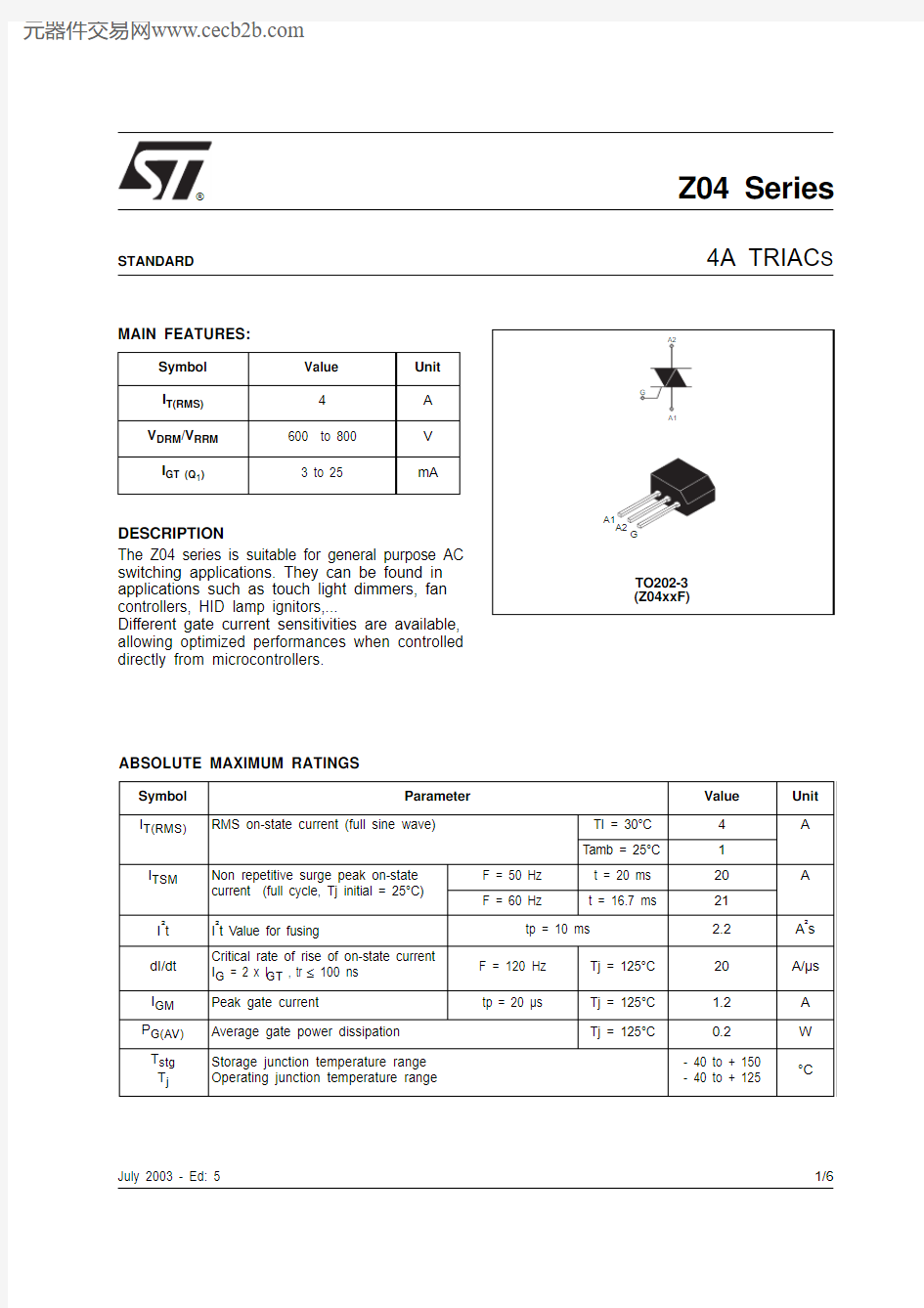
MAIN FEATURES:
DESCRIPTION
The Z04 series is suitable for general purpose AC switching applications. They can be found in applications such as touch light dimmers, fan controllers, HID lamp ignitors,...
Different gate current sensitivities are available,allowing optimized performances when controlled directly from microcontrollers.
Symbol Value Unit I T(RMS)4A V DRM /V RRM 600 to 800V I GT (Q 1)
3 to 25
mA
ABSOLUTE MAXIMUM RATINGS
Symbol Parameter
Value Unit I T(RMS)RMS on-state current (full sine wave)
TI = 30°C 4A
Tamb = 25°C
1I TSM Non repetitive surge peak on-state current (full cycle, Tj initial = 25°C) F = 50 Hz t = 20 ms 20A F = 60 Hz
t = 16.7 ms
21I 2t I 2t Value for fusing
tp = 10 ms
2.2
A 2
s dI/dt Critical rate of rise of on-state current I G = 2 x I GT , tr ≤ 100 ns F = 120 Hz Tj = 125°C 20A/μs I GM Peak gate current
tp = 20 μs
Tj = 125°C 1.2A P G(AV)Average gate power dissipation Tj = 125°C
0.2W T stg T j
Storage junction temperature range Operating junction temperature range
- 40 to + 150- 40 to + 125
°C
Z04 Series
2/6
ELECTRICAL CHARACTERISTICS (Tj = 25°C, unless otherwise specified)
STATIC CHARACTERISTICS
Note 1: minimum IGT is guaranted at 5% of IGT max.Note 2: for both polarities of A2 referenced to A1
THERMAL RESISTANCES
Symbol Test Conditions
Quadrant
Z04xx Unit
02
050910I GT (1)V D = 12 V R L = 30 ?
ALL MAX.3
510
25
mA V GT ALL MAX. 1.3V V GD V D = V DRM R L = 3.3 k ? Tj = 125°C ALL
MIN.0.2
V I H (2)I T = 50 mA MAX.351025mA I L I G = 1.2 I GT
I - III - IV
MAX.
6101525mA II
12152550dV/dt (2)V D = 67 %V DRM gate open Tj = 110°C MIN.1020100200V/μs (dV/dt)c (2)
(dI/dt)c = 1.8 A/ms Tj = 110°C
MIN.
0.5
1
2
5
V/μs
Symbol Test Conditions
Value Unit V TM (2)I TM = 5.5 A tp = 380 μs Tj = 25°C MAX. 2.0V V to (2)Threshold voltage Tj = 125°C MAX.0.95V R d (2)Dynamic resistance Tj = 125°C MAX.180m ?I DRM I RRM
V DRM = V RRM
Tj = 25°C MAX.
5μA Tj = 125°C
0.5
mA
Symbol Parameter
Value Unit R th(j-l)Junction to lead (AC)15°C/W R th(j-a)
Junction to ambient
100
°C/W
Z04 Series
3/6
PRODUCT SELECTOR
ORDERING INFORMATION
OTHER INFORMATION
Note: xx = sensitivity, y = voltage
Part Number
Voltage Sensitivity
Type
Package
600 V
700 V
800 V
Z0402MF X
3 mA Standard TO202-3Z0402SF X
3 mA Standard TO202-3Z0402NF X
3 mA Standard TO202-3Z0405MF X
5 mA Standard TO202-3Z0405SF X
5 mA Standard TO202-3Z0405NF X
5 mA Standard TO202-3Z0409MF X
10 mA Standard TO202-3Z0409SF X
10 mA Standard TO202-3Z0409NF X
10 mA Standard TO202-3Z0410MF X
25 mA Standard TO202-3Z0410SF X
25 mA Standard TO202-3Z0410NF
X
25 mA
Standard
TO202-3
Part Number
Marking
Weight Base quantity Packing mode Z04xxyF 0AA2Z04xxyF 0.8 g 50Tube Z04xxyF 1AA2
Z04xxyF
0.8 g
250
Bulk
Z04 Series
4/6
Fig. 1: Maximum power dissipation versus RMS on-state current (full cycle).
Fig. 2: RMS on-state current versus ambient temperature (full cycle).
Fig. 3: Relative variation of thermal impedance junction to ambient versus pulse duration.
Fig. 4: Relative variation of gate trigger current,holding current and latching current versus junction temperature (typical values).
Fig. 5: Surge peak on-state current versus number of cycles.
Fig. 6: Non-repetitive surge peak on-state current for a sinusoidal pulse with width tp <10ms, and corresponding value of I2t.
Z04 Series
5/6
Fig. 7: On-state characteristics (maximum values).
Fig. 8: Relative variation of critical rate of decrease of main current versus (dV/dt)c (typical values).
Fig. 9: Relative variation of critical rate of decrease of main current versus junction temperature.
Z04 Series
PACKAGE MECHANICAL DATA
Information furnished is believed to be accurate and reliable. However, STMicroelectronics assumes no responsibility for the consequences of use of such information nor for any infringement of patents or other rights of third parties which may result from its use. No license is granted by implication or otherwise under any patent or patent rights of STMicroelectronics. Specifications mentioned in this publication are subject to change without notice. This publication supersedes and replaces all information previously supplied. STMicroelectronics products are not authorized for use as critical components in life support devices or systems without express written approval of STMicroelectronics.
? The ST logo is a registered trademark of STMicroelectronics
? 2003 STMicroelectronics - Printed in Italy - All Rights Reserved
STMicroelectronics GROUP OF COMPANIES
Australia - Brazil - China - Finland - France - Germany - Hong Kong - India - Italy - Japan - Malaysia
Malta - Morocco - Singapore - Spain - Sweden - Switzerland - United Kingdom - U.S.A
https://www.360docs.net/doc/3a5410322.html,
6/6