LM3410中文资料

ADVANCE INFORMATION
October 2007 LM3410
525kHz/1.6MHz, Constant Current Boost and SEPIC LED Driver with Internal Compensation
General Description
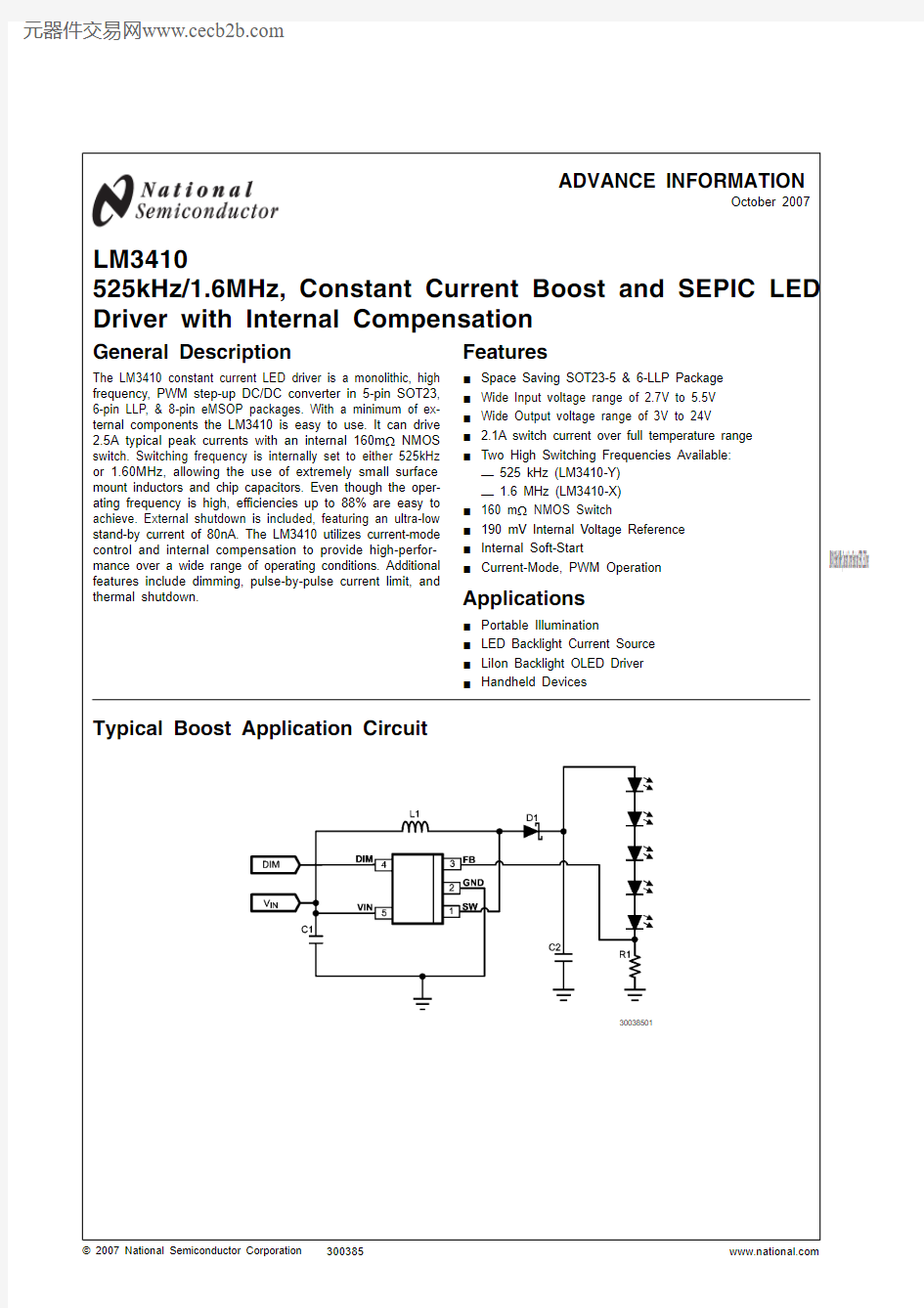
The LM3410 constant current LED driver is a monolithic, high frequency, PWM step-up DC/DC converter in 5-pin SOT23, 6-pin LLP, & 8-pin eMSOP packages. With a minimum of ex-ternal components the LM3410 is easy to use. It can drive 2.5A typical peak currents with an internal 160m? NMOS switch. Switching frequency is internally set to either 525kHz or 1.60MHz, allowing the use of extremely small surface mount inductors and chip capacitors. Even though the oper-ating frequency is high, efficiencies up to 88% are easy to achieve. External shutdown is included, featuring an ultra-low stand-by current of 80nA. The LM3410 utilizes current-mode control and internal compensation to provide high-perfor-mance over a wide range of operating conditions. Additional features include dimming, pulse-by-pulse current limit, and thermal shutdown.Features
■Space Saving SOT23-5 & 6-LLP Package
■Wide Input voltage range of 2.7V to 5.5V
■Wide Output voltage range of 3V to 24V
■ 2.1A switch current over full temperature range ■Two High Switching Frequencies Available:—525 kHz (LM3410-Y)
—1.6 MHz (LM3410-X)
■160 m? NMOS Switch
■190 mV Internal Voltage Reference
■Internal Soft-Start
■Current-Mode, PWM Operation Applications
■Portable Illumination
■LED Backlight Current Source
■LiIon Backlight OLED Driver
■Handheld Devices
Typical Boost Application Circuit
30038501
? 2007 National Semiconductor https://www.360docs.net/doc/316782535.html, LM3410 525kHz/1.6MHz, Constant Current Boost and SEPIC LED Driver
Connection Diagrams
Top View
30038503
5-Pin SOT23
Top View
30038504
6-Pin LLP
Top View
30038505
8-Pin eMSOP
Ordering Information
Frequency
Order Number Package Type Package Drawing
Supplied As 525 kHz
LM3410YMF SOT23-5MF05A 1000 units tape & reel LM3410YMFX
3000 units tape & reel LM3410YSD LLP-6SDE06A 1000 units tape & reel LM3410YSDX 4500 units tape & reel LM3410YMY eMSOP-8MUY08A 1000 units tape & reel LM3410YMYX 3500 units tape & reel 1.6 MHz
LM3410XMF SOT23-5MF05A 1000 units tape & reel LM3410XMFX
3000 units tape & reel LM3410XSD LLP-6SDE06A 1000 units tape & reel LM3410XSDX 4500 units tape & reel LM3410XMY eMSOP-8
MUY08A
1000 units tape & reel LM3410XMYX
3500 units tape & reel
https://www.360docs.net/doc/316782535.html, 2
L M 3410
Pin Description - 5-Pin SOT23
Pin Name Function
1SW Output switch. Connect to the inductor, output diode.
2GND Signal and power ground pin. Place the bottom resistor of the feedback network as close as possible to this pin.
3FB Feedback pin. Connect FB to external resistor divider to set output voltage.
4DIM Dimming & shutdown control input. Logic high enables operation. Duty Cycle from 0 to 100%. Do not allow this pin to float or be greater than VIN + 0.3V.
5VIN Supply voltage for power stage, and input supply voltage.
Pin Description - 6 Pin LLP
Pin Name Function
1PGND Power ground pin. Place PGND and output capacitor GND close together.
2VIN Supply voltage for power stage, and input supply voltage.
3DIM Dimming & shutdown control input. Logic high enables operation. Duty Cycle from 0 to 100%. Do not allow this pin to float or be greater than VIN + 0.3V.
4FB Feedback pin. Connect FB to external resistor divider to set output voltage.
5AGND Signal ground pin. Place the bottom resistor of the feedback network as close as possible to this pin & pin 4.
6SW Output switch. Connect to the inductor, output diode.
DAP GND Signal & Power ground. Connect to pin 1 & pin 5 on top layer. Place 4-6 vias from DAP to bottom layer GND plane.
Pin Description - 8 Pin eMSOP
Pin Name Function
1-No Connect
2PGND Power ground pin. Place PGND and output capacitor GND close together.
3VIN Supply voltage for power stage, and input supply voltage.
4DIM Dimming & shutdown control input. Logic high enables operation. Duty Cycle from 0 to 100%. Do not allow this pin to float or be greater than VIN + 0.3V.
5FB Feedback pin. Connect FB to external resistor divider to set output voltage.
6AGND Signal ground pin. Place the bottom resistor of the feedback network as close as possible to this pin & pin 5 7SW Output switch. Connect to the inductor, output diode.
8-No Connect
DAP GND Signal & Power ground. Connect to pin 2 & pin 6 on top layer. Place 4-6 vias from DAP to bottom layer GND plane.
https://www.360docs.net/doc/316782535.html,
LM3410
Physical Dimensions inches (millimeters) unless otherwise noted
6-Lead LLP Package
NS Package Number SDE06A
5-Lead SOT23-5 Package NS Package Number MF05A
https://www.360docs.net/doc/316782535.html, 4
L M 3410
LM3410 8-Lead eMSOP Package
NS Package Number MUY08A
https://www.360docs.net/doc/316782535.html,
Notes
L M 3410 525k H z /1.6M H z , C o n s t a n t C u r r e n t B o o s t a n d S E P I C L E D D r i v e r
THE CONTENTS OF THIS DOCUMENT ARE PROVIDED IN CONNECTION WITH NATIONAL SEMICONDUCTOR CORPORATION (“NATIONAL”) PRODUCTS. NATIONAL MAKES NO REPRESENTATIONS OR WARRANTIES WITH RESPECT TO THE ACCURACY OR COMPLETENESS OF THE CONTENTS OF THIS PUBLICATION AND RESERVES THE RIGHT TO MAK E CHANGES TO SPECIFICATIONS AND PRODUCT DESCRIPTIONS AT ANY TIME WITHOUT NOTICE. NO LICENSE, WHETHER EXPRESS,IMPLIED, ARISING BY ESTOPPEL OR OTHERWISE, TO ANY INTELLECTUAL PROPERTY RIGHTS IS GRANTED BY THIS DOCUMENT.
TESTING AND OTHER QUALITY CONTROLS ARE USED TO THE EXTENT NATIONAL DEEMS NECESSARY TO SUPPORT NATIONAL’S PRODUCT WARRANTY. EXCEPT WHERE MANDATED BY GOVERNMENT REQUIREMENTS, TESTING OF ALL PARAMETERS OF EACH PRODUCT IS NOT NECESSARILY PERFORMED. NATIONAL ASSUMES NO LIABILITY FOR APPLICATIONS ASSISTANCE OR BUYER PRODUCT DESIGN. BUYERS ARE RESPONSIBLE FOR THEIR PRODUCTS AND APPLICATIONS USING NATIONAL COMPONENTS. PRIOR TO USING OR DISTRIBUTING ANY PRODUCTS THAT INCLUDE NATIONAL COMPONENTS, BUYERS SHOULD PROVIDE ADEQUATE DESIGN, TESTING AND OPERATING SAFEGUARDS.
EXCEPT AS PROVIDED IN NATIONAL’S TERMS AND CONDITIONS OF SALE FOR SUCH PRODUCTS, NATIONAL ASSUMES NO LIABILITY WHATSOEVER, AND NATIONAL DISCLAIMS ANY EXPRESS OR IMPLIED WARRANTY RELATING TO THE SALE AND/OR USE OF NATIONAL PRODUCTS INCLUDING LIABILITY OR WARRANTIES RELATING TO FITNESS FOR A PARTICULAR PURPOSE, MERCHANTABILITY, OR INFRINGEMENT OF ANY PATENT, COPYRIGHT OR OTHER INTELLECTUAL PROPERTY RIGHT.
LIFE SUPPORT POLICY
NATIONAL’S PRODU CTS ARE NOT AU THORIZED FOR U SE AS CRITICAL COMPONENTS IN LIFE SU PPORT DEVICES OR SYSTEMS WITHOU T THE EXPRESS PRIOR WRITTEN APPROVAL OF THE CHIEF EXECU TIVE OFFICER AND GENERAL COUNSEL OF NATIONAL SEMICONDUCTOR CORPORATION. As used herein:
Life support devices or systems are devices which (a) are intended for surgical implant into the body, or (b) support or sustain life and whose failure to perform when properly used in accordance with instructions for use provided in the labeling can be reasonably expected to result in a significant injury to the user. A critical component is any component in a life support device or system whose failure to perform can be reasonably expected to cause the failure of the life support device or system or to affect its safety or effectiveness.
National Semiconductor and the National Semiconductor logo are registered trademarks of National Semiconductor Corporation. All other brand or product names may be trademarks or registered trademarks of their respective holders.
Copyright? 2007 National Semiconductor Corporation
For the most current product information visit us at https://www.360docs.net/doc/316782535.html,
National Semiconductor Americas Customer Support Center Email:
new.feedback@https://www.360docs.net/doc/316782535.html, Tel: 1-800-272-9959
National Semiconductor Europe Customer Support Center Fax: +49 (0) 180-530-85-86
Email: europe.support@https://www.360docs.net/doc/316782535.html, Deutsch Tel: +49 (0) 69 9508 6208English Tel: +49 (0) 870 24 0 2171Fran?ais Tel: +33 (0) 1 41 91 8790
National Semiconductor Asia Pacific Customer Support Center Email: ap.support@https://www.360docs.net/doc/316782535.html,
National Semiconductor Japan Customer Support Center Fax: 81-3-5639-7507
Email: jpn.feedback@https://www.360docs.net/doc/316782535.html, Tel: 81-3-5639-7560
https://www.360docs.net/doc/316782535.html,