FS5ASJ-3-T13中文资料
FS5ASJ-3
High-Speed Switching Use Nch Power MOS FET
REJ03G1406-0200
(Previous: MEJ02G0077-0101)
Rev.2.00 Aug 07, 2006
Features
? Drive voltage : 4 V ? V DSS : 150 V
? r DS(ON) (max) : 0.35 ? ? I D : 5 A
?
Integrated Fast Recovery Diode (TYP.) : 85 ns
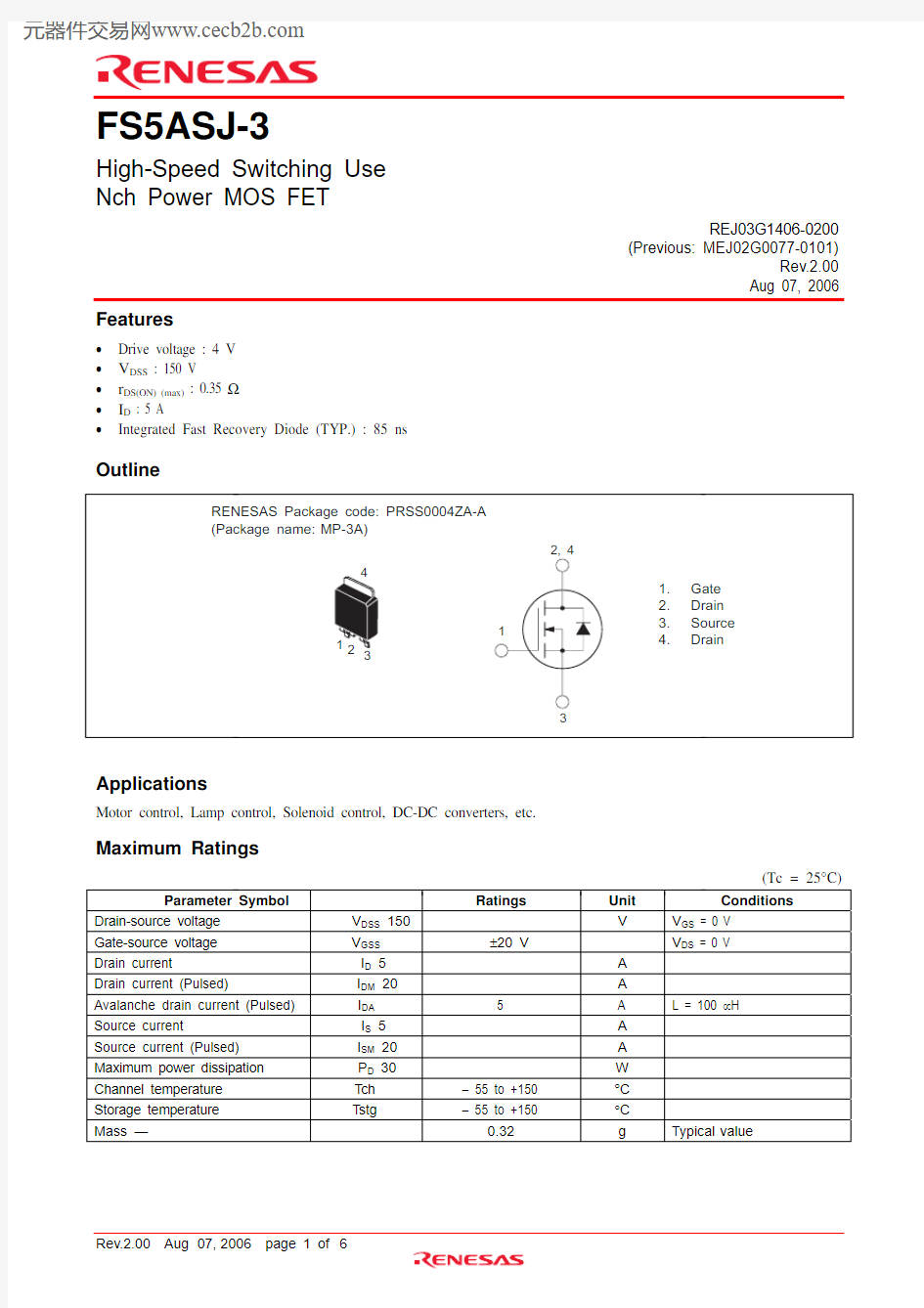
Outline
RENESAS Package code: PRSS0004ZA-A (Package name: MP-3A)
1. Gate
2. Drain
3. Source
4. Drain
1
13
3
2, 4
2
4
Applications
Motor control, Lamp control, Solenoid control, DC-DC converters, etc.
Maximum Ratings
(Tc = 25°C)
Parameter Symbol Ratings Unit Conditions
Drain-source voltage V DSS 150 V V GS = 0 V Gate-source voltage V GSS ±20 V V DS = 0 V Drain current I D 5 A Drain current (Pulsed) I DM 20 A Avalanche drain current (Pulsed) I DA 5 A L = 100 μH Source current I S 5 A Source current (Pulsed) I SM 20 A Maximum power dissipation P D 30 W Channel temperature Tch – 55 to +150 °C Storage temperature Tstg – 55 to +150 °C Mass — 0.32 g Typical value
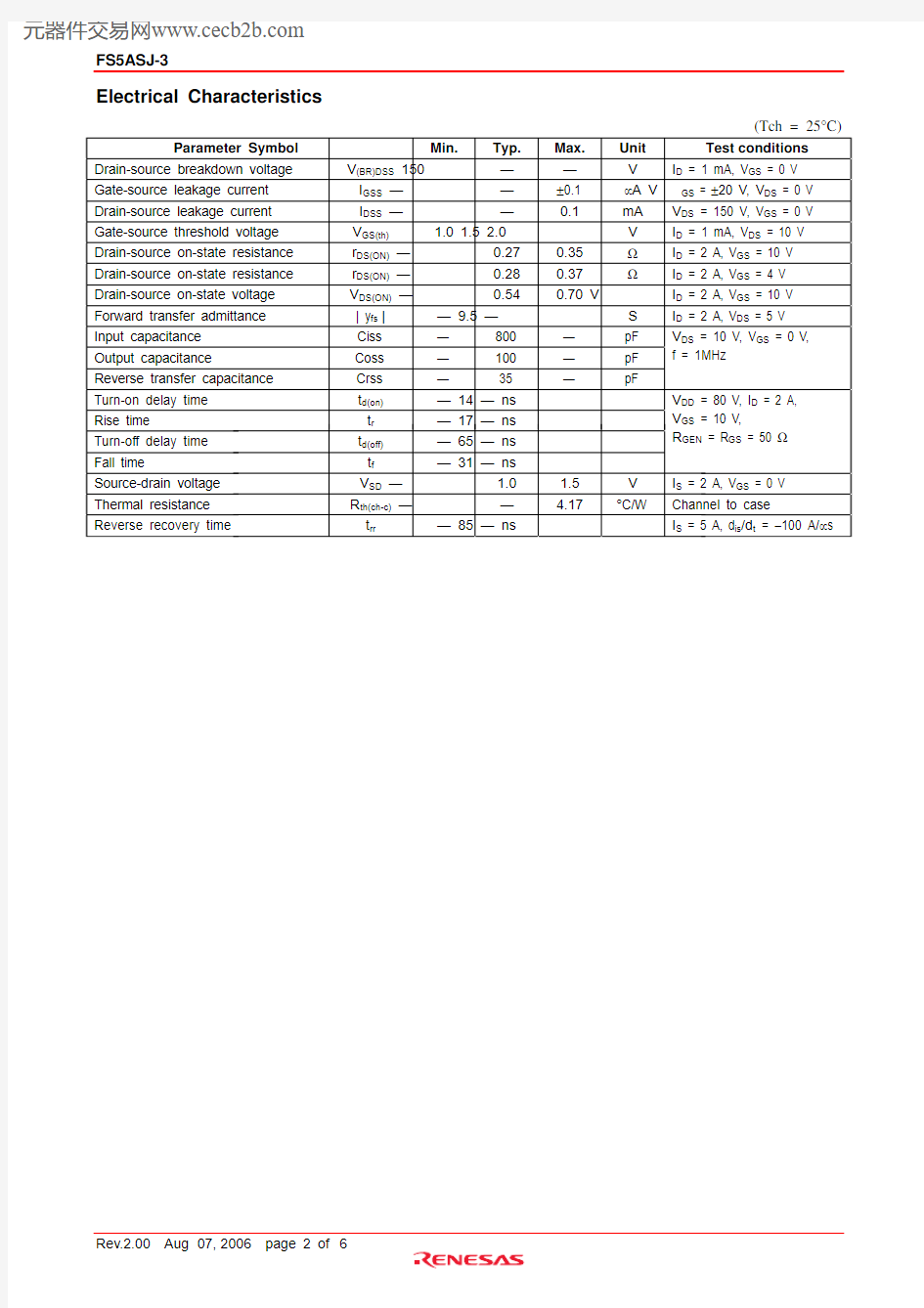
Electrical Characteristics
(Tch = 25°C)
Parameter Symbol Min. Typ. Max. Unit Test conditions
Drain-source breakdown voltage V (BR)DSS 150 — — V I D = 1 mA, V GS = 0 V Gate-source leakage current I GSS — — ±0.1 μA V GS = ±20 V, V DS = 0 V Drain-source leakage current I DSS — — 0.1 mA V DS = 150 V, V GS = 0 V Gate-source threshold voltage V GS(th) 1.0 1.5 2.0 V I D = 1 mA, V DS = 10 V Drain-source on-state resistance r DS(ON) — 0.27 0.35 ? I D = 2 A, V GS = 10 V Drain-source on-state resistance r DS(ON) — 0.28 0.37 ? I D = 2 A, V GS = 4 V Drain-source on-state voltage V DS(ON) — 0.54 0.70 V I D = 2 A, V GS = 10 V Forward transfer admittance | y fs | — 9.5 — S I D = 2 A, V DS = 5 V Input capacitance Ciss — 800 — pF Output capacitance Coss — 100 — pF Reverse transfer capacitance
Crss — 35 — pF
V DS = 10 V, V GS = 0 V,
f = 1MHz Turn-on delay time t d(on) — 14 — ns Rise time
t r — 17 — ns
Turn-off delay time t d(off) — 65 — ns
Fall time
t f — 31 — ns V DD = 80 V, I D = 2 A,
V GS = 10 V, R GEN = R GS = 50 ? Source-drain voltage V SD — 1.0 1.5 V I S = 2 A, V GS = 0 V Thermal resistance R th(ch-c) — — 4.17 °C/W Channel to case Reverse recovery time t rr — 85 — ns I S = 5 A, d is /d t = –100 A/μs
Performance Curves
Case Temperature Tc (°C)Drain-Source Voltage V Output Characteristics (Typical)
Drain-Source Voltage V DS (V)Output Characteristics (Typical)
D r a i n C u r r e n t I D (A )
Drain-Source Voltage V On-State Voltage vs.
Gate-Source Voltage (Typical)
On-State Resistance vs.Drain Current (Typical)
S (O N ) (?)
1.0
2.0
3.0
4.0
5.0
V GS = 10V 4V 3.5V
2.5V
3V
2V
P D = 30W
1.0
2.03.04.05.0
00.40.8 1.2V GS = 10V 4V 0.5Tc = 25°C Pulse Test
Tc = 25°C Pulse Test
Tc = 25°C Pulse Test
Tc = 25°C Pulse Test
Switching Characteristics (Typical)
Drain-Source Voltage V DS (V)
Capacitance vs.
Drain-Source Voltage (Typical)
Drain Current I S w i t c h i n g T i m e (n s )
Gate-Source Voltage vs.Gate Charge (Typical)
Source-Drain Diode Forward Characteristics (Typical)
A )
1002101357210235732Ciss
Coss
Crss
10
–1100
23457210110223457103234571620
Tch = 25°C f = 1MHz = 0V
Tch = 25V DD = 80V V GS = 10V
R GEN = R Tch = 25°C = 5A V GS = 0V Pulse Test
Transient Thermal Impedance Characteristics
Channel Temperature Tch (°C)Breakdown Voltage vs.Channel Temperature (Typical)
Pulse Width tw (s)
T r a n s i e n t T h e r m a l I m p e d a n c e Z t h (c h –c ) (°C /W )
Switching Time Measurement Circuit
Switching Waveform
Vin Monitor D.U.T.
Vout Monitor
050100150
10–11002
3571012
357
102235710–4
235723572357235710–310–210–1D = 1.00.50.2
0.10.050.020.01
Single Pulse
= 0V = 1mA
Package Dimensions
0.5 ± 0.2
0.76
0.76 ± 0.2 2.3 ± 0.2
1.4 ±
2.3
1
Order Code
Lead form
Standard packing
Quantity
Standard order code
Standard order code example
Surface-mounted type Taping 3000Type name – T +Direction (1 or 2) +3 FS5ASJ-3-T13 Surface-mounted type Plastic Magazine (Tube) 75Type name FS5ASJ-3 Note : Please confirm the specification about the shipping in detail.
https://www.360docs.net/doc/3d10916807.html, RENESAS SALES OFFICES
Refer to "https://www.360docs.net/doc/3d10916807.html,/en/network" for the latest and detailed information.
Renesas Technology America, Inc.
450 Holger Way, San Jose, CA 95134-1368, U.S.A
Tel: <1> (408) 382-7500, Fax: <1> (408) 382-7501
Renesas Technology Europe Limited
Dukes Meadow, Millboard Road, Bourne End, Buckinghamshire, SL8 5FH, U.K.
Tel: <44> (1628) 585-100, Fax: <44> (1628) 585-900
Renesas Technology (Shanghai) Co., Ltd.
Unit 204, 205, AZIACenter, No.1233 Lujiazui Ring Rd, Pudong District, Shanghai, China 200120
Tel: <86> (21) 5877-1818, Fax: <86> (21) 6887-7898
Renesas Technology Hong Kong Ltd.
7th Floor, North Tower, World Finance Centre, Harbour City, 1 Canton Road, Tsimshatsui, Kowloon, Hong Kong
Tel: <852> 2265-6688, Fax: <852> 2730-6071
Renesas Technology Taiwan Co., Ltd.
10th Floor, No.99, Fushing North Road, Taipei, Taiwan
Tel: <886> (2) 2715-2888, Fax: <886> (2) 2713-2999
Renesas Technology Singapore Pte. Ltd.
1 Harbour Front Avenue, #06-10, Keppel Bay Tower, Singapore 098632
Tel: <65> 6213-0200, Fax: <65> 6278-8001
Renesas Technology Korea Co., Ltd.
Kukje Center Bldg. 18th Fl., 191, 2-ka, Hangang-ro, Yongsan-ku, Seoul 140-702, Korea
Tel: <82> (2) 796-3115, Fax: <82> (2) 796-2145
Renesas Technology Malaysia Sdn. Bhd
Unit 906, Block B, Menara Amcorp, Amcorp Trade Centre, No.18, Jalan Persiaran Barat, 46050 Petaling Jaya, Selangor Darul Ehsan, Malaysia
Tel: <603> 7955-9390, Fax: <603> 7955-9510
? 2006. Renesas Technology Corp., All rights reserved. Printed in Japan.