UCN5815EPTR中文资料
D
I S C O N T I N U E D P R O D U C T —
F O R R E
F E
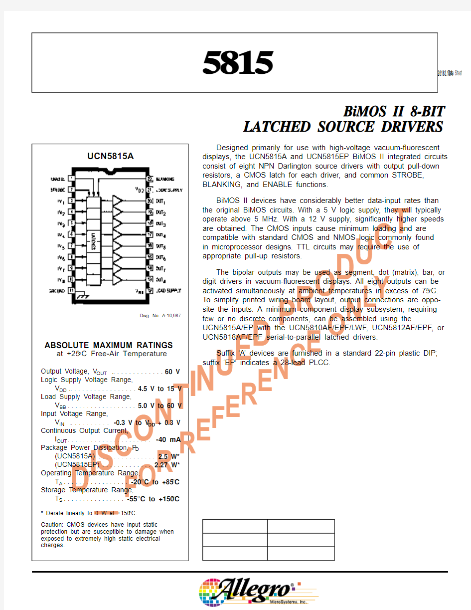
R E N C E O N L Y Designed primarily for use with high-voltage vacuum-fluorescent displays, the UCN5815A and UCN5815EP BiMOS II integrated circuits consist of eight NPN Darlington source drivers with output pull-down resistors, a CMOS latch for each driver, and common STROBE,BLANKING, and ENABLE functions.
BiMOS II devices have considerably better data-input rates than the original BiMOS circuits. With a 5 V logic supply, they will typically operate above 5 MHz. With a 12 V supply, significantly higher speeds are obtained. The CMOS inputs cause minimum loading and are compatible with standard CMOS and NMOS logic commonly found in microprocessor designs. TTL circuits may require the use of appropriate pull-up resistors.
The bipolar outputs may be used as segment, dot (matrix), bar, or
digit drivers in vacuum-fluorescent displays. All eight outputs can be activated simultaneously at ambient temperatures in excess of 75°C.To simplify printed wiring board layout, output connections are oppo-site the inputs. A minimum component display subsystem, requiring few or no discrete components, can be assembled using the
UCN5815A/EP with the UCN5810AF/EPF/LWF, UCN5812AF/EPF, or UCN5818AF/EPF serial-to-parallel latched drivers.
Suffix ‘A’ devices are furnished in a standard 22-pin plastic DIP;suffix ‘EP’ indicates a 28-lead PLCC.
BiMOS II 8-BIT
LATCHED SOURCE DRIVERS
UCN5815A
Dwg. No. A-10,987
ABSOLUTE MAXIMUM RATINGS
at +25°C Free-Air Temperature
Output Voltage, V OUT .. . . . . . . . . . . . . 60 V Logic Supply Voltage Range,
V DD .. . . . . . . . . . . . . . . . . 4.5 V to 15 V Load Supply Voltage Range,
V BB . . . . . . . . . . . . . . . . . . 5.0 V to 60 V Input Voltage Range,
V IN .. . . . . . . . . . -0.3 V to V DD + 0.3 V Continuous Output Current,
I OUT . . . . . . . . . . . . . . . . . . . . . . -40 mA Package Power Dissipation, P D
(UCN5815A). . . . . . . . . . . . . . . 2.5 W*(UCN5815EP). . . . . . . . . . . . . 2.27 W*Operating Temperature Range,
T A . . . . . . . . . . . . . . . . . -20°C to +85°C Storage Temperature Range,
T S . . . . . . . . . . . . . . . . -55°C to +150°C
* Derate linearly to 0 W at +150°C.
Caution: CMOS devices have input static
protection but are susceptible to damage when exposed to extremely high static electrical charges.
Data Sheet
26183.10A
5815
5815BiMOS II
8-BIT LATCHED
SOURCE DRIVERS
115 Northeast Cutoff, Box 15036
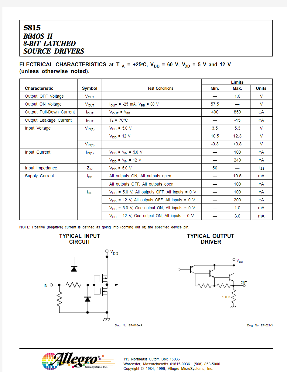
Worcester, Massachusetts 01615-0036 (508) 853-5000ELECTRICAL CHARACTERISTICS at T A = +25°C, V BB = 60 V, V DD = 5 V and 12 V (unless otherwise noted).
Limits Characteristic Symbol Test Conditions Min.Max.Units Output OFF Voltage V OUT — 1.0V Output ON Voltage V OUT I OUT = -25 mA, V BB = 60 V 57.5—V Output Pull-Down Current I OUT V OUT = V BB 400850μA Output Leakage Current I OUT T A = 70°C —-15μA Input Voltage
V IN(1)
V DD = 5.0 V 3.5 5.3V V DD = 12 V
10.512.3V V IN(0)
-0.3+0.8V Input Current
I IN(1)
V DD = V IN = 5.0 V —100μA V DD = V IN = 12 V
—240μA Input lmpedance Z IN V DD = 5.0 V
50—k ?Supply Current
l BB
All outputs ON, All outputs open —10.5
mA All outputs OFF, All outputs open
—100μA l DD
V DD = 5.0 V, All outputs OFF, All inputs = 0 V —100μA V DD = 12 V, All outputs OFF, All inputs = 0 V —200μA V DD = 5.0 V, One output ON, All inputs = 0 V — 1.0mA V DD = 12 V, One output ON, All inputs = 0 V
—
3.0
mA
NOTE: Positive (negative) current is defined as going into (coming out of) the specified device pin.
TYPICAL INPUT
CIRCUIT
TYPICAL OUTPUT
DRIVER
Dwg. No. EP-021-3
W
Copyright ? 1984, 1996, Allegro MicroSystems, Inc.
5815
BiMOS II 8-BIT LATCHED
SOURCE DRIVERS
UCN5815EP
Dwg. No. A-14,357
Information present at an input is trans-
ferred to its latch when the STROBE and
ENABLE are high. The latches will continue
to accept new data as long as both STROBE
and ENABLE are held high. With either
STROBE or ENABLE in the low state, no
information can be loaded into the latches.
When the BLANKING input is high, all of
the output buffers are disabled (OFF) without
affecting the information stored in the
latches. With the BLANKING input low, the
outputs are controlled by the state of the
latches.
The timing conditions shown above
guarantee a 4.4 MHz minimum data input
rate with a 5 V supply. Typically, input rates
above 5 MHz are permitted. With a 12 V
supply, rates in excess of 10 MHz are
possible.
X = irrelevant
T-1 = previous output state
T = present output state
TRUTH TABLE
5815BiMOS II
8-BIT LATCHED
SOURCE DRIVERS
115 Northeast Cutoff, Box 15036
Worcester, Massachusetts 01615-0036 (508) 853-5000
UCN5815A
Dimensions in Inches
NOTES: 1.Exact body and lead configuration at vendor ’s option within limits shown.
2.Lead spacing tolerance is non-cumulative.
3.Lead thickness is measured at seating plane or below.
5815BiMOS II
8-BIT LATCHED SOURCE DRIVERS
UCN5815EP
Dimensions in Inches (controlling dimensions
NOTES: 1.Exact body and lead configuration at vendor ’s option within limits shown.
2.Lead spacing tolerance is non-cumulative.
Dimensions in Millimeters (for reference only)
5815BiMOS II
8-BIT LATCHED
SOURCE DRIVERS
115 Northeast Cutoff, Box 15036
Worcester, Massachusetts 01615-0036 (508) 853-5000
BiMOS II (Series 5800) & DABiC IV (Series 6800)INTELLIGENT POWER INTERFACE DRIVERS
SELECTION GUIDE
Function
Output Ratings *
Part Number ?
SERIAL-INPUT LATCHED DRIVERS
8-Bit (saturated drivers)-120 mA 50 V?58958-Bit 350 mA 50 V 58218-Bit 350 mA 80 V 58228-Bit 350 mA 50 V?58418-Bit 350 mA 80 V?58429-Bit
1.6 A 50 V 5829
10-Bit (active pull-downs)-25 mA 60 V 5810-F and 6809/1012-Bit (active pull-downs)-25 mA 60 V 5811 and 681120-Bit (active pull-downs)-25 mA 60 V 5812-F and 681232-Bit (active pull-downs)-25 mA 60 V 5818-F and 681832-Bit
100 mA 30 V 583332-Bit (saturated drivers)
100 mA
40 V
5832
PARALLEL-INPUT LATCHED DRIVERS
4-Bit 350 mA 50 V?58008-Bit -25 mA 60 V 58158-Bit
350 mA
50 V?
5801
SPECIAL-PURPOSE FUNCTIONS
Unipolar Stepper Motor Translator/Driver 1.25 A 50 V?5804Addressable 28-Line Decoder/Driver
450 mA 30 V 6817
*Current is maximum specified test condition, voltage is maximum rating. See specification for sustaining voltage limits.Negative current is defined as coming out of (sourcing) the output.
?Complete part number includes additional characters to indicate operating temperature range and package style.?
Internal transient-suppression diodes included for inductive-load protection.
Allegro MicroSystems, Inc. reserves the right to make, from time to time, such departures from the detail specifications as may be required to permit improvements in the design of its products.
The information included herein is believed to be accurate and reliable. However, Allegro MicroSystems, Inc. assumes no
responsibility for its use; nor for any infringements of patents or other rights of third parties which may result from its use.