LM5073MHNOPB;LM5073MHXNOPB;LM5073HE-EVAL;中文规格书,Datasheet资料
LM5073
LM5073 100V Power Over Ethernet PD Interface with Aux Support
Literature Number: SNVS490B
LM5073
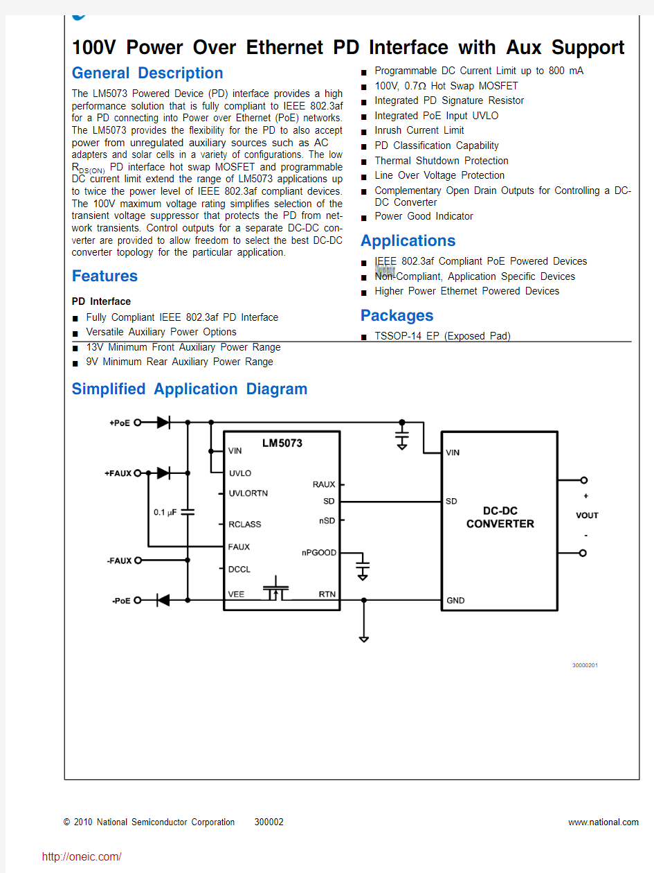
100V Power Over Ethernet PD Interface with Aux Support General Description
The LM5073 Powered Device (PD) interface provides a high
performance solution that is fully compliant to IEEE 802.3af
for a PD connecting into Power over Ethernet (PoE) networks.
The LM5073 provides the flexibility for the PD to also accept
power from unregulated auxiliary sources such as AC
adapters and solar cells in a variety of configurations. The low
R
DS(ON) PD interface hot swap MOSFET and programmable
DC current limit extend the range of LM5073 applications up to twice the power level of IEEE 802.3af compliant devices. The 100V maximum voltage rating simplifies selection of the transient voltage suppressor that protects the PD from net-work transients. Control outputs for a separate DC-DC con-verter are provided to allow freedom to select the best DC-DC converter topology for the particular application. Features
PD Interface
■Fully Compliant IEEE 802.3af PD Interface
■Versatile Auxiliary Power Options
■13V Minimum Front Auxiliary Power Range
■9V Minimum Rear Auxiliary Power Range ■Programmable DC Current Limit up to 800 mA
■100V, 0.7? Hot Swap MOSFET
■Integrated PD Signature Resistor
■Integrated PoE Input UVLO
■Inrush Current Limit
■PD Classification Capability
■Thermal Shutdown Protection
■Line Over Voltage Protection
■Complementary Open Drain Outputs for Controlling a DC-DC Converter
■Power Good Indicator
Applications
■IEEE 802.3af Compliant PoE Powered Devices
■Non-Compliant, Application Specific Devices
■Higher Power Ethernet Powered Devices Packages
■TSSOP-14 EP (Exposed Pad)
Simplified Application Diagram
30000201
? 2010 National Semiconductor https://www.360docs.net/doc/4a2385256.html, 5073 100V Power Over Ethernet PD Interface with Aux Support
30000202
14 Lead TSSOP-EP
Ordering Information
Order Number Package Type NSC Package Drawing
Supplied As LM5073MH TSSOP-14EP MXA14A 94 Units per Rail
LM5073MHX
TSSOP-14EP
MXA14A
2500 Units on Tape and Ree
Pin Descriptions
Pin Number
Name Description
1UVLORTN Return for the external UVLO programming resistor divider.2UVLO Line under-voltage lockout programming pin.3VIN Positive supply pin for the PD interface and the DC-DC converter interface.
4RCLASS PD Classification programming pin.5FAUX Front auxiliary power enable pin.
6DCCL PD interface DC current limit programming pin.
7VEE Negative supply pin for the PD interface; connected to PoE and/or front auxiliary power return path.8NC No internal connection.
9RTN DC-DC converter power return; connected to the drain of the internal PD interface hot swap MOSFET.10NC No internal connection.
11nPGOOD PD interface power good delay and indicator. nPGOOD is low when the ho swap MOSFET drain to source voltage is less than 1.5V.
12nSD Open drain, active low shut down signal to the DC-DC converter. The nSD p switches to the high impedance state when nPGOOD is less than 2.5V.
13SD Open drain, active high shut down signal to the DC-DC converter. The SD p switches to the low state when nPGOOD is less than 2.5V.
14RAUX Rear auxiliary power enable pin, and dominant/non-dominant selection.
EP
Exposed metal pad on the underside of the device. It is recommended to connect this pad to a PC Board plane connected to the VEE pin to improve heat dissipation.
https://www.360docs.net/doc/4a2385256.html, 2
L
If Military/Aerospace specified devices are required, please contact the National Semiconductor Sales Office/ Distributors for availability and specifications.
VIN, FAUX, UVLO, RTN to VEE
(Note 6)-0.3V to 100V UVLORTN to VEE-0.3V to 16V DCCL, RCLASS to VEE-0.3V to 7V nPGOOD, nSD, SD to RTN-0.3V to 16V RAUX to RTN-0.3V to 100V
ESD Rating
Human Body Model (Note 2)2000V Lead Soldering Temp. (Note 3)
Wave (4 seconds)
Infrared (10 seconds)
Vapor Phase (75 seconds)
260°C
240°C
219°C Storage Temperature-55°C to 150°C Junction Temperature150°C Operating Ratings
V
IN
voltage9V to 70V Operating Junction Temperature-40°C to 125°C
Electrical Characteristics (Note 4)Limits in standard type are for T
J
= 25°C only; limits in boldface type apply
over the junction temperature (T
J
) range of -40°C to +125°C. Minimum and Maximum limits are guaranteed through test, design,
or statistical correlation. Typical values represent the most likely parametric norm at T
J
= 25°C, and are provided for reference
purposes only. V
IN
= 48V unless otherwise indicated. (Note 3)
Symbol Parameter Conditions Min Typ Max Units Supply Current
VIN Supply Current Normal Operation23mA Detection and Classification
VIN Signature Startup Voltage 1.5V
Signature Resistance23.2524.526k?
Signature Resistor Disengage / Classification Engage V
IN
Rising11.01212.8V Hysteresis 1.9V
Classification Current Turn Off V
IN
Rising2223.525V RCLASS Voltage 1.213 1.25 1.287V
Supply Current During Classification V
IN
= 17V0.7 1.1mA
Line Under Voltage Lock-Out
Default UVLO Release V
IN
Rising3638.540V
Default UVLO Lock out V
IN
Falling29.53132.5V Default UVLO Hysteresis6V
Programmed UVLO Reference Voltage V
IN
> 12.5V 1.2 1.24 1.28V
Programmed UVLO Hysteresis Current V
IN
> UVLO162024μA
UVLORTN Pull Down Resistance V
IN
> 12.5V55150?UVLO Filter300μs
Power Good
VDS Required for Power Good Status 1.3 1.5 1.7V
VDS Hysteresis of Power Good Status0.81 1.2V
VGS Required for Power Good Status 4.5 5.5 6.5V
Default Delay Time of Loss-of Power Good Status30μs
nPGOOD Current Source405570μA
nPGOOD Open circuit Voltage 3.54 5.5V
nPGOOD Pull Down Resistance180300?
nPGOOD Threshold2 2.53V Shutdown Outputs
nSD/SD Pull Down Resistance180300?
Leakage nSD/SD = 16V1μA
https://www.360docs.net/doc/4a2385256.html,
73
Hot Swap
RDS(ON)Hot Swap MOSFET Resistance0.7 1.5 Hot Swap MOSFET Leakage100μ
Inrush Current Limit V
DS
= 4.0V120150180m
Default DC Current Limit V
DS
= 4.0V380440510m
High DC Current Limit V
DS
= 4.0V690800930m
Current Limit Programming Accuracy V
DS
= 4.0V-1212
Hot Swap Over-Voltage Protection
VIN OVP Threshold606570
VIN OVP Threshold, Hysteresis3
Auxiliary Power Option
FAUX Threshold8.18.79.5
FAUX Hysteresis0.5
FAUX Pull Down Current50μ
RAUX Lower Threshold (I = 22 μA)RAUX Pin Rising 2.3 2.7 3.4
RAUX Lower Threshold Hysteresis0.8
RAUX Upper Threshold (I = 250 μA)RAUX Pin Rising 5.4 6.27.4
RAUX Lower Threshold Current142230μ
RAUX Upper Threshold Current170250330μPDI Thermal Shutdown (Note 5)
Thermal Shutdown Temperature165°
Thermal Shutdown Hysteresis20°Thermal Resistance
θJA Junction to Ambient MXA Package40°C
Note 1:Absolute Maximum Ratings are limits beyond which damage to the device may occur. Operating Ratings are conditions under which operation of the device is intended to be functional. For guaranteed specifications and test conditions, see the Electrical Characteristics.
Note 2:The human body model is a 100 pF capacitor discharged through a 1.5 k? resistor into each pin.
Note 3:For detailed information on soldering the plastic TSSOP package, refer to the Packaging Databook available from National Semiconductor.
Note 4:Minimum and Maximum limits are guaranteed through test, design, or statistical correlation using Statistical Quality Control (SQC) methods. Typical
values represent the most likely parametric norm at T
J = 25°C, and are provided for reference purpose only. Limits are used to calculate National’s Average
Outgoing Quality Level (AOQL).
Note 5:Device thermal limitations may limit usable range.
Note 6:During rear auxiliary operation, the RTN pin can be approximately -0.4V with respect to VEE. This is caused by normal internal bias currents, and w not harm the device. Application of external voltage or current must not cause the absolute maximum rating to be exceeded.
https://www.360docs.net/doc/4a2385256.html,4
L
Default UVLO Threshold vs Temperature 30000203DC Current Limit vs. DCCL Resistor
30000204
Inrush Current Limit vs Temperature 30000205Programmed DC Current Limit vs Temperature
30000206
Default DC Current Limit vs Temperature 30000207
Input Current vs Input Voltage
30000208
https://www.360docs.net/doc/4a2385256.html,
73
30
FIGURE 1. LM5073 Top Level Block Diagram
Description of Operation and Applications Information
The LM5073 integrates a fully IEEE 802.3af compliant PD in-terface with versatile auxiliary power support. When com-bined with a separate DC-DC converter, it provides a complete power solution for Powered Devices (PD) that con-nect to PoE systems.
The LM5073 provides the following features:
1.The input voltage rating up to 100V allows greater
flexibility when selecting a transient surge suppressor to protect the PD from voltage transients encountered in PoE applications.
2.
The integration of the PD signature resistor, inrush current limit, programmable input voltage under-voltag lock-out (UVLO), PD classification, and thermal shutdown simplifies PD implementation.
3.
The PD interface accepts power from auxiliary source including AC adapters and solar cells in various configurations over a wide range of input voltages.Auxiliary power input can be programmed to be either non-dominant or dominant over PoE power.4.Programmable DC current limit to support PD
applications requiring input currents up to 800 mA.5.
Complementary open drain outputs for controlling a D DC converter.
https://www.360docs.net/doc/4a2385256.html, 6
L
driving a power good indicator LED.
7.Input line over voltage protection for downstream circuits,
including the DC-DC converter.
DC-DC Converter Selection
A PD designed with LM5073 can be optimized for a variety of applications by selecting the DC-DC converter from a wide range of topologies. Topology selection enables several de-sign trade-offs including efficiency, complexity, and cost. For example, the LM5025 controller for the Active Clamp For-ward topology can be paired with the LM5073 for increased efficiency, especially at higher power levels. In cases where isolation is not required an LM5576 regulator with a built in buck switch provides a simple, low cost solution.
The 100V capability of the LM5073 protects against input voltage transients, especially in the case of a hot swapping front auxiliary power. The LM5073 has built-in over-voltage protection such that a DC-DC converter with input voltage rating as low as 65V can be safely used.
The DC-DC converter must have a soft start feature to control the input current during startup. The soft-start process re-duces the surge of inrush current and eliminates any tenden-cy of the output voltage to overshoot during startup. The DC current limit or the current limit of the PSE, otherwise the PD will not start correctly.
Modes of Operation
Per the IEEE 802.3af specification, when a PD is connected to a PoE system it transitions through several operating modes in sequence including detection, classification (op-tional), turn-on inrush, and normal DC operation. Each oper-ating mode corresponds to a specific voltage range supplied from the PSE. Figure 2 shows the IEEE 802.3af specified se-quence of operating modes and the corresponding PD input voltages at the RJ-45 connector.
Current steering diode bridges are required for the PD inter-face to accept all allowable connections and polarities of PoE voltage from the RJ-45 connector (see the example applica-tion circuit in Figure 11). The bridge voltage drop will reduce the input voltage sensed by the LM5073. To guarantee full compliance to the specification in all operating modes, the LM5073 takes into account the voltage drop across the bridge diodes and responds appropriately to the voltage received from the PoE cable. Table 1 presents the response in each operating mode to voltages at the PD input connector and between the VIN and VEE pins.
30000210
FIGURE 2. Sequence of PoE Operating Modes TABLE 1. Operating Modes With Respect To Input Voltage
Mode of Operation Voltage at PD Input Connector per
IEEE 802.3af LM5073 Input Voltage (VIN pin to VEE pin)
Detection (Signature) 2.7V to 10.1V 1.5V to 10.0V Classification14.5V to 20.5V12V to 23.5V
Startup Threshold42V max38V (UVLO Release, VIN Rising)
Normal Operation36V to 57V65V to 32V (UVLO, VIN Falling)
https://www.360docs.net/doc/4a2385256.html, 73
In the detection mode, a PD must present a signature resis-tance between 23.75 k ? and 26.25 k ? to the PoE power sourcing equipment. This signature impedance distinguishes the PD from non-PoE equipment to protect the latter from be-ing accidentally damaged by inadvertent application of PoE voltage levels. To simplify the circuit implementation, the LM5073 integrates the signature resistor, as shown in Figure 3.
During the detection mode, the voltage across the VIN and VEE pins is less than 10V. Once detection mode is complete,the LM5073 will disengage the signature resistor to reduce power loss in all other modes.
30000211
FIGURE 3. Detection Circuit With Integrated PD Signature
Resistor
Classification is an optional feature of the IEEE 802.3af spe ification. It is primarily used to identify the power requiremen of a particular PD. This feature will allow the PSE to alloca the appropriate available power to each device on the n work. Classification is performed by measuring the curre flowing into the PD during this mode. IEEE 802.3af specifi five power classes, each corresponding to a unique range classification current, as presented in Table 2. As shown Figure 4, the LM5073 simplifies the classification impleme tation by requiring a single external resistor connected b tween the RCLASS and VEE pins to program the classific tion current. The resistor value required for each class is al given in Table 2.
During the classification mode, the voltage between the V and VEE pins is between 12V and 23.5V. In this volta range, the class resistor R CLASS is engaged by enabling t 1.25V buffer amplifier and MOSF ET. After classification complete, the voltage from the PSE will increase to the norm operating voltage of the PoE system (48V nominal). Wh VIN rises above 23.5V, the LM5073 will disengage t RCLASS resistor to reduce on-chip power dissipation.The classification feature is disabled when either the front rear auxiliary power options are selected, as the classificati function is not required when power is supplied from an au iliary source. The classification function is also disabled wh the LM5073 reaches the thermal shutdown temperatu threshold (nominally 165°C). This may occur if the LM5073operated at elevated ambient temperatures and the class cation time exceeds the IEEE 802.3af limit of 75 ms.
When the classification option is not required, simply lea the RCLASS pin open to set the PD to the default Class state. Class 0 requires that the PSE allocate the maximu IEEE 802.3af specified power of 15.4W (12.95W at the P input terminals) to the PD.
TABLE 2. Classification Levels and Required External Resistor Value
Class PD Max Power Level I CLASS Range
LM5073R CLASS Value
From To From To 0 (Default)
0.44W 12.95W 0 mA 4 mA Open 10.44W 3.84W 9 mA 12 mA 130?2 3.84W 6.49W 17 mA 20 mA 71.5?3 6.49W 12.95W 26 mA 30 mA 46.4?4
Reserved
Reserved
36 mA
44 mA
31.6?
https://www.360docs.net/doc/4a2385256.html, 8
L
30000212
FIGURE 4. PD Classification – Fulfilled With a Single External Resistor
Undervoltage Lockout (UVLO)
The LM5073 contains both programmable and default input Under Voltage Lock Out (UVLO) circuits. Figure 5 illustrates the block diagram of the LM5073 UVLO circuit. When the UVLO pin is connected to the VIN pin the internal default thresholds and hysteresis are selected, requiring no external components to comply with the IEEE 802.3af UVLO specifi-cations. To program the UVLO threshold and hysteresis to custom values, use two external resistors R1 and R2. Con-necting an external resistor divider to the UVLO pin automat-ically overrides the default UVLO settings.
The LM5073’s UVLO circuit continuously monitors the PoE input voltage between the VIN and VEE pins. When the VIN voltage rises above the upper threshold, either default or pro-grammed, the UVLO circuit will enable the hot swap MOSFET and initiate the startup inrush sequence. During normal op-erating mode, when the VIN voltage falls below the default or the programmed lower threshold, the LM5073 disables the PD by disabling the hot swap MOSFET. A built-in 300 μs timer delays the disable signal, to prevent disabling the hot swap MOSFET during intermittent transients.
The UVLO thresholds are determined by the following con-siderations. The PD can draw a maximum current of 400 mA during IEEE 802.3af PoE operation. This current will cause a voltage drop of up to 8V over a 100m long Ethernet cable. The PD front-end current steering diode bridges may introduce an additional 2V drop. To guarantee successful startup at the minimum PoE voltage of 42V and to continue operation at the minimum requirement of 36V, as specified by IEEE 802.3af,
these voltage drops must be taken into account. Accordingly,the LM5073 UVLO default thresholds are set to 38V, on the rising edge of VIN, and 31V on the falling edge of VIN. The 7V nominal hysteresis of the default UVLO function, along with the inrush current limit (discussed in the next section),prevents false starts and chattering during startup.
In addition to the default settings, the UVLO threshold and hyteresis can be programmed independently to custom val-ues. After selecting R1 to program the UVLO hysteresis, the ratio between R1 and R2 determines the UVLO threshold.The resistors should be selected to satisfy the following rela-tionships:
R1 = V HYS / 20 μA
Where V UVLO is the upper (positive going) trip point and V HYS is the difference betweeen the upper and lower trip points.
The UVLO thresholds should not be programmed below the classification threshold or above the OVP threshold.
The UVLO signal will be overridden by the front auxiliary pow-er option (see details in the FAUX section).
The UVLO function can also be used to implement a remote enable / disable function. Pulling the UVLO pin down below the UVLO threshold disables the interface and the control outputs for the DC-DC converter.
https://www.360docs.net/doc/4a2385256.html,
73
分销商库存信息:
NATIONAL-SEMICONDUCTOR
LM5073MH/NOPB LM5073MHX/NOPB LM5073HE-EVAL