Recent Developments in 3-D Imaging Technologies
Recent Developments in 3-D Imaging Technologies
Jung-Young Son,Bahram Javidi ,Fellow,IEEE ,Sumio Yano,and Kyu-Hwan Choi
Abstract—Three-dimensional (3D)imaging technologies that have been developed recently are reviewed.In recent years,many new progresses in the 3D imaging have been made but most of them provide more practical solutions to comply with the commer-cialization efforts of the 3D imaging.Based on time-multiplexing,revisiting the stereoscopic imaging methods is one of the solutions to make possible each view image has the full panel resolution.The rapid progresses of high speed LCDs and the initiation of stereoscopic imaging service to mobile phones have made the method possible.The efforts also encouraged more concerns in evaluating 3-D image quality and identifying factors affecting the quality.In this respect,in-depth analysis has been done for the multiview imaging methods,and other forms of multiview 3D image display methods,such as the focused image/pixel array of multiview images are also analyzed.
Index Terms—Continuous parallax,focused image array,full resolution stereoscopic imaging,holographic imaging,image quality,multiview 3D,3D imaging technologies,time-multiplexing.
I.I NTRODUCTION
S
TEREOSCOPIC and multiview images are still consid-ered as the most adaptable methods to the current plane imaging systems,among the currently known three-dimensional (3D)imaging methods [1]–[6].This is why commercialization efforts have been concentrated on the stereoscopic and mul-tiview images for the last several years by the major display companies in the world.However,the full volume market for the 3D image displays is still some distance away.This is not because of the lack of 3D imaging services and contents but because the quality of 3D images is usually somewhat worse than that of plane images,which is now in the super High Def-inition (HD)level.The resolution of super HD is four times higher than that of Full HD
(19201080),which is considered as having a remarkable image quality.This is probably why major display companies are interested in stereoscopic imaging with full display panel resolution [7]–[10]more than the mul-tiview 3D.The recent development of high speed LCD which is capable of operating 240-Hz frame rate makes feasible the stereoscopic imaging.This LCD is used either as display panel
Manuscript received December 01,2009;revised March 01,2010;accepted March 02,2010.
J.-Y.Son is with the School of Computer and Communication Engineering,Daegu University,Kyungsan,Kyungbuk,Korea (e-mail:sjy4271@hanyang.ac.kr).
B.Javidi is with the Department of Electrical and Computer En-gineering,University of Connecticut,Storrs,CT 06268USA (e-mail:bahram@https://www.360docs.net/doc/403250948.html,).
S.Yano is with the National Institute of Information and Communications Technology (NICT),Keihana,Kyoto 619-0289,Japan,(e-mail:yano.s@nict.go.jp).
K.-H.Choi is with Samsung Advanced Institute of Technology (SAIT),Yongin,Gyeonggi,Korea (e-mail:kh0715.choi@https://www.360docs.net/doc/403250948.html,).
Color versions of one or more of the ?gures in this paper are available online at https://www.360docs.net/doc/403250948.html,.
Digital Object Identi?er 10.1109/JDT.2010.2045636
or parallax barrier.In the display panel,left and right eye im-ages are switched time-sequentially to display stereoscopic im-ages with each view image having full display panel resolution.The time sequential display method is especially advantageous to the displays with a very limit resolution,as in mobile phones.The stereoscopic image service for the mobile phones has al-ready been provided,but the typical resolution of LCD panel mounted on the mobile phones,
320240is too small to display the stereoscopic images in a spatial multiplexing fashion [11].The time-sequential method allows making
320240image resolution for each view image in the mobile displays.
Compared with the stereoscopic image,3D images based on the multiview images have been considered as providing more natural depth sense and comfort to viewers.But the resolution of each view image is low compared with the panel resolution and becomes lower as the number of different view images to be displayed increases.To mitigate this problem,either many low resolution projectors such as pico-projectors or many high res-olutions projectors as a focused light beam array of multiview images are used [12],[13].Using more projectors,the resolu-tion of each view image is not even further increased but also the number of multiview images.These approaches are paving to achieve a super-multiview image [1].But the cost of building them will be very high and aligning the projectors requires much more efforts than other multiview 3-D imaging methods at least for now.These problems will be aggravated more as the number of the projectors increases.Hence,multiview imaging methods [4]are at least for now not given much consideration for com-mercialization by the major display companies.The commer-cialization efforts are also urged to develop proper methods for evaluating and improving 3D image quality and re?ning prob-lems related with current 3D imaging method [14]–[17].For this purpose,activities for developing guidelines for 3D dis-plays based on ergonomics and for standardization of technical and biomedical speci?cations for the display have been initial-ized [14].In addition to the activities,an experiment to make ?t the ?at panel displays to 3D has also been performed [18].This has a signi?cant meaning because 3D displays are getting out from the subordinate relationship to ?at panel displays.In the electro-holographic imaging areas,only few new developments related with fast calculation algorithm for CGH (Computer Gen-erated Hologram)have been reported [19]–[21].But recording and displaying 3D natural scene based on fringe pattern calcu-lation with the image depth information obtained from a depth camera [22]or a multiview camera array [23]are an impres-sive new result.From these developments,it is not dif?cult to imagine that super-multiview and holography based 3D imaging methods,and new ?at panels for the methods will be the major subjects for the future 3D imaging research.
In this paper,3D imaging methods developed recently,and other developments related with existing 3D imaging methods,are reviewed.The priority given to this paper is providing
1551-319X/$26.00?2010IEEE
in-depth information regarding the underlying principles of those methods.However,the 3D imaging methods reviewed in the previous articles [1],[2]are only brie?y mentioned whenever they are necessary.
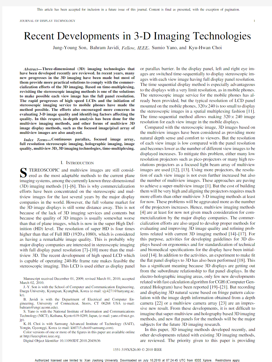
II.D ISPLAY C HARACTERISTICS OF P LANE AND 3D I MAGES In general,all plane image displaying screens and panels are diffusing the images to their front space to increase viewing space,though the diffusing angles are different for different screens and panels.Hence,when two different plane images are displayed simultaneously based on a spatial multiplexing scheme or are displayed time sequentially based on a time-mul-tiplexing scheme,they look mixed because the images are blurred as shown in Fig.1(a).There are a couple of ways to make these images be separately viewed:One is making each of these images have different optical characteristics to each other and the other to have different viewing directions,as shown in Fig.1(b).The former is for the eyeglasses type stereoscopic imaging methods,such as color ?lter (anaglyph),polarization and shuttering (transparency change),and the latter is for the multiview 3D imaging methods including non-eyeglasses type stereoscopic imaging methods [2].For the case of the former,since two images with different optical characteristics are coex-isting in the viewing space,each view image will be selectively viewed through a media which is transparent to the optical characteristic of the image.When the optical characteristic of the media composing a side of the eyeglasses is matched with that of one of the two images and the other side with the other image,the eyeglasses become transparent and the two images will be perceived as an image with a certain depth if the images are from a stereoscopic image pair.By this way the media in each side of the eyeglasses is directing the image to the eye behind the media.Hence,the eyeglasses is used to create viewing regions for separately viewing each of the two images.For the latter case,each view image is optically directed to a de?ned direction so that it is not mixed with other view images and viewed at a speci?c viewing direction.This direction will have a small range because rays composing the image are diverging.There are several ways of directing each view image to its de?ned direction,such as using a viewing zone forming optics (VZFO),a point light source array[24],a focused point array of multiview images [12],[13],a point array of multiview pixels [25]and a collimated image array[26].The VZFO is composed of an array of elemental optics.This elemental optics is typically a pinhole,a microlens,a line slit and a long cylindrical lens.The VZFO can have other forms such as grating array,Fresnel lens,holographic screen,micro-retarder .But recently,
micro-retarder lenticular [17],a varifocal lens [27]and a tunable microlens array made of liquid crystal [28],and micromirror arrays [29],[30]are also introduced.The VZFO is attached in front of the display panel to use its optical power to separate each view image from the multiview images displayed on the panel and direct it to (a)de?ned direction(s)to create its viewing region(s)in its front space.It also works as the image projection screen for projection type.However,the vari-focal lens aligns each frame image on the display panel to focus at different depths to create a volumetric image.The eyeglasses for stereoscopic images are movable forms of VZFO because viewers can move around within the viewing
space.
Fig.1.Diffused (plane)and directed (3D)images.
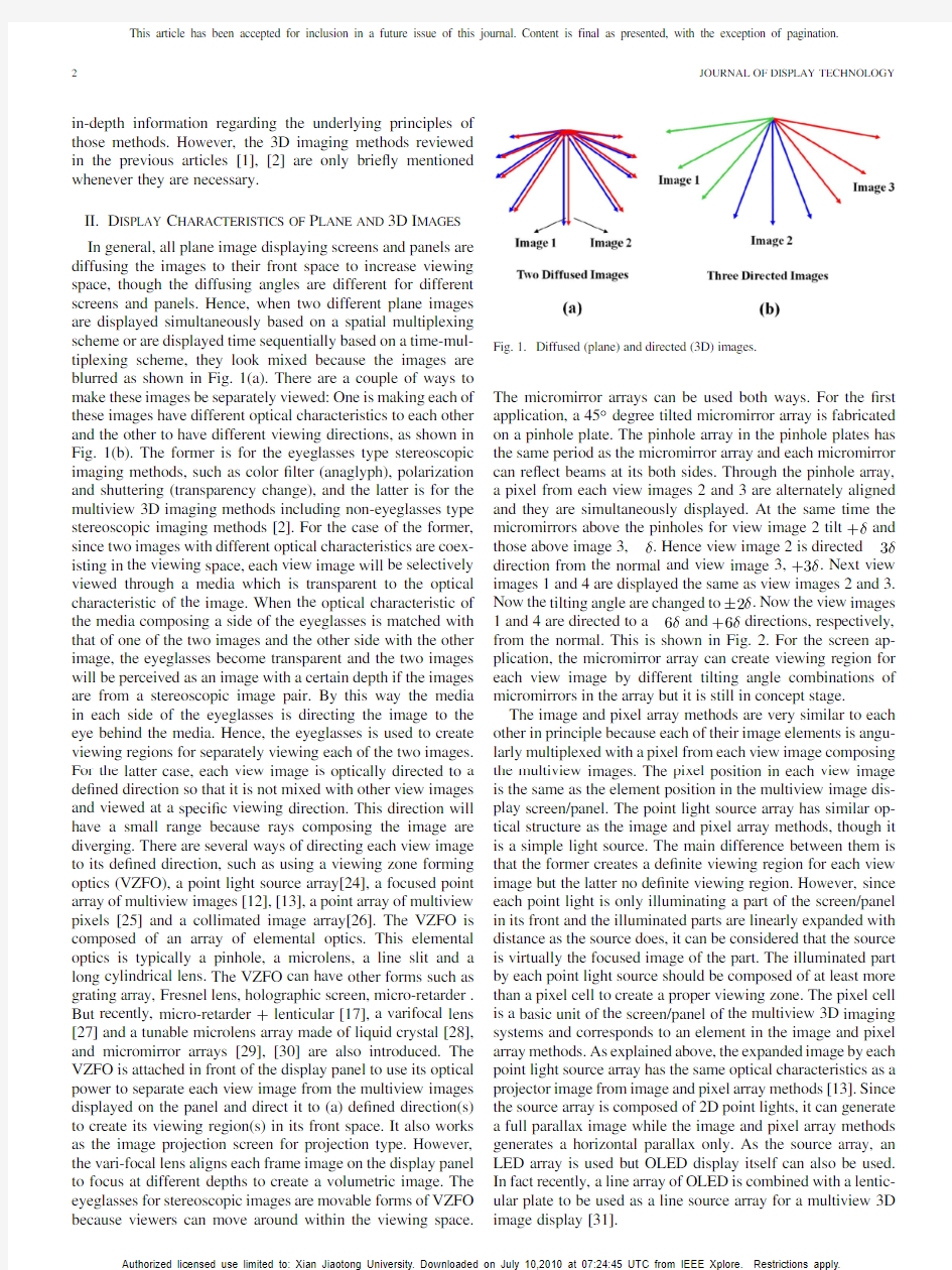
The micromirror arrays can be used both ways.For the ?rst application,a 45degree tilted micromirror array is fabricated on a pinhole plate.The pinhole array in the pinhole plates has the same period as the micromirror array and each micromirror can re?ect beams at its both sides.Through the pinhole array,a pixel from each view images 2and 3are alternately aligned and they are simultaneously displayed.At the same time the
micromirrors above the pinholes for view image 2
tilt
and those above image 3,.Hence view image 2is
directed direction from the normal and view image
3,.Next view images 1and 4are displayed the same as view images 2and 3.
Now the tilting angle are changed
to
.Now the view images 1and 4are directed to
a
and directions,respectively,from the normal.This is shown in Fig.2.For the screen ap-plication,the micromirror array can create viewing region for each view image by different tilting angle combinations of micromirrors in the array but it is still in concept stage.
The image and pixel array methods are very similar to each other in principle because each of their image elements is angu-larly multiplexed with a pixel from each view image composing the multiview images.The pixel position in each view image is the same as the element position in the multiview image dis-play screen/panel.The point light source array has similar op-tical structure as the image and pixel array methods,though it is a simple light source.The main difference between them is that the former creates a de?nite viewing region for each view image but the latter no de?nite viewing region.However,since each point light is only illuminating a part of the screen/panel in its front and the illuminated parts are linearly expanded with distance as the source does,it can be considered that the source is virtually the focused image of the part.The illuminated part by each point light source should be composed of at least more than a pixel cell to create a proper viewing zone.The pixel cell is a basic unit of the screen/panel of the multiview 3D imaging systems and corresponds to an element in the image and pixel array methods.As explained above,the expanded image by each point light source array has the same optical characteristics as a projector image from image and pixel array methods [13].Since the source array is composed of 2D point lights,it can generate a full parallax image while the image and pixel array methods generates a horizontal parallax only.As the source array,an LED array is used but OLED display itself can also be used.In fact recently,a line array of OLED is combined with a lentic-ular plate to be used as a line source array for a multiview 3D image display [31].
SON et al.:RECENT DEVELOPMENTS IN 3-D IMAGING TECHNOLOGIES
3
Fig.2.Multiview image display by double-sided mirror
array.
Fig.3.Recording geometry of Zebra hologram.
The quality of the multiview 3D images is related with the number of pixel cells and pixels in each pixel cell/element.These numbers increases,the quality improves.They can be hardly increased with currently available ?at panel displays but the focused point array methods can because they can use a projector array or angularly multiplexed multi-pixel point array.The number of different view images and resolution of each view image will be increased by aligning more number of and higher resolution projectors or pixel points.Though there is no convinceable evidence yet but it has been considered that increasing the number of different view images and their resolution can also display a hologram like image as shown by Zebra hologram [32].The Zebra hologram is a stereo hologram and consists of a 2-D pixilated hologram array recorded on a photopolymer.Each pixilated hologram is named as hogel and made by focusing a very high resolution image to a point as in the holographic memory [33].Fig.3shows the recording geometry of the Zebra hologram.Each of a multiview image array is displayed on a spatial light modulator and illuminated with a converging laser beam to record it as a point hologram on a photoplate.By shifting the photoplate in both horizontal and vertical directions according to the relative position of each view image in the multiview image array,a point hologram array corresponding to the multiview image array is formed on
the photoplate.The reconstructed image of the Zebra hologram is consisted of a point array of focused images.Each of the focused image point in the array will be diverging with the angle the same as the focused angle for recording.Hence the reconstructed image will not be different from the displayed image of the image and pixel array methods.Instead of using photopolymer,photorefractive polymer can be used [34].This material is rewritable and has a high density,the refreshable Zebra hologram can be recorded on the media.
III.P ROGRESSES IN S TEREOSCOPIC I MAGES
The conventional multiview 3D imaging methods including stereoscopic imaging had a critical disadvantage of sharing the resolution of a display panel with the multiview images to be displayed together for the 3D image display.Due to this sharing,the resolution of each view image is reduced to the value cor-responding to the display resolution divided by the number of different view images within the multiview images.This is one of reasons reducing the 3D image quality.To overcome this problem,full panel resolution stereoscopic imaging methods based on time-multiplexing have been developed to improve the quality of stereoscopic images to the level of plane images.The methods are especially useful for mobile phone displays which are with low resolution displays.The methods can be realized
4JOURNAL OF DISPLAY
TECHNOLOGY
Fig.4.Principle of displaying a stereoscopic image with full panel resolution.
three different ways:1)combining two high speed?at display panels as image display and VZFO,respectively;2)one high speed?at panel for image display and directional light guides, for non-eyeglasses type;and3)one high speed?at panel for image display and high speed shutter glasses as VZFO for eye-glasses type.The working principle of the high speed VZFO method is depicted in Fig.4.A high speed LCD panel for VZFO is creating a parallax barrier.For the starting,the images are interlaced with right and left image order but next the order is reversed with shifting open slit of the parallax barrier to a half period to the left as shown in Fig.4.For the next periods these two sequences are repeating.Since this sequence is re-peated more than120Hz,right and left images have the full resolution of the image panel without?ickering.For the case of the eyeglasses-type,the whole image panel displays left-right or right–left image order and a high speed LCD shutter glasses ON-OFF sequences of the right and left sides are synchronized with the image display order.In this shuttering process,to min-imize the crosstalk caused by LCD relaxation time,shutter ON time is set slightly shorter than the OFF time.For the case of using directional light guides,VZFO is not necessary because the light guide directs the illuminating lights for right eye image to the right eye direction and for left eye image to left.The light guides have been made by making grooves on the bottom sur-face of a plastic plate[35]and patterning prismatic and lentic-ular structure on a plastic?lm[36].The former case,the groove depths are increasing and periods are decreasing as the distance from the light source increases.The latter case,the guide has the structure of a lenticular sheet on the top of a light guide.The bottom of the lenticular sheet is grooved with a prism array.In these systems LED is used for the light source.Left and right LEDs lit alternately and their working periods are synchronized with the images on LCD panel.
There are several other developments in stereoscopic images.
A volumetric stereo image display[37]and non-eyeglasses-type polarization based stereoscopic displays[17],[38].The volu-metric stereo image display is providing the real image depth to the stereoscopic images by seeing each eye image through a focal length controllable lens assembly.The image displayed on the display panel imaged to the distance corresponding to the stereoscopically induced depth by controlling the focal
length Fig.5.Non-eyeglasses-type full panel resolution stereoscopic image display based on lenticular+microretarder.
of the lens assembly.In this way,the image depth becomes the same as the perceived image depth,i.e.,vergence and accommo-dation are provided.The stereoscopic displays have two exam-ples;one is using a micro-retarder plate combined with a lentic-ular plate and the other is using viewing zone limiting aperture. The former is essentially a directional light guide type stereo-scopic imaging method using polarized lights.Micro-retarder+ lenticular is functionally generating directional beams for left and right eye images.Fig.5shows the structure of the display. The lights from back light panel are polarized in a certain direc-tion.These polarized lights are passing through a polarization switch.This switch is to rotate the polarization direction of the incoming light to90when it is operating.After passing the switch,the lights are passed a strip-type micro-retarder.In this retarder,zero and half wavelength strip retarders are alternately aligned.The half wave retarder strips rotate the polarization di-rections of incoming lights90.After the retarder,the lights are passing the lenticular plate.Since the width of each cylindrical lens in the lenticular plate is slightly less than that of a strip pair, the magni?ed images of the same retarding strips are converged
SON et al.:RECENT DEVELOPMENTS IN 3-D IMAGING TECHNOLOGIES
5
https://www.360docs.net/doc/403250948.html,parison of principles of hologram and photo taking.
to space as shown in Fig.5.The zero retarder strip images are converged to the right-hand side and half wave strip images to the left side.These two retarder strip images have 90polar-ization difference.If the LCD panel polarizer has the same po-larization direction as one of the images,only this image will pass the LCD.The other image is completely blocked by the LCD because of 90polarization difference.Hence,the image on LCD will be seen at the space where the image is converging.Next,the polarization switch changes the incoming light’s po-larization direction.Then the polarization direction of the other image is matched to that of the LCD panel polarizer.The LCD panel image is now seen at the other side.Hence,it is possible to display full panel resolution stereoscopic images based on time multiplexing.The latter is basically a stereoscopic images based on a spatial multiplexing.For full panel resolution,two displays are combined by a half mirror for to view the displays at a common direction.To direct each display to its corresponding eye,the polarization directions of two panels are 90different to each other and a polarized eyeglasses is needed.Instead of using the eyeglasses,the common direction is blocked by locating two polarizer pieces side by side.The polarization direction of each piece is the same as that of its corresponding display panel.Then these pieces are imaged by a concave mirror to form viewing zone and the images on the two panels are imaged by a lens to the mirror.The display part can be replaced by
a –pole LCD.IV .C HARACTERISTICS OF M ULTIVIEW 3D I MAGE AND
H OLOGRAPHIC I MAGE
In the physical optics including hologram,the object depth is transformed into phase.Hence to preserve the depth informa-tion in the hologram,phase should be recorded.In the hologram,phase is recorded as interference patterns formed by interfering two coherent beams.i.e.,reference and object beams [39].For the two objects of different distances,the phase difference be-tween the rays from the longer distance object and the refer-ence beam will be smaller than those for the other object.This is because the beam incidence angle to the photoplate for the near distance object is bigger than for the far distance object.Hence hologram can reconstruct original object image with the real depth.Hologram is also providing continuous parallax [40].The continuous parallax means that the parallax value of an ob-ject in the hologram is not a discrete but continuously changing when viewers move their eyes from a point to another point in the hologram as viewers see things in their living environments.This is possible in the hologram because the object information is recorded on the entire hologram surface.
In contrast to the hologram,the multiview images comprise no phase information and continuous parallax.The difference between taking a hologram and a photo is depicted in Fig.6.For the case of the hologram,a photoplate located at the en-trance pupil of the camera objective records re?ected rays from the various surface of the object to the whole pupil plane by in-terfering the rays with a reference beams.The reference and illu-minating beam to the object should be originated from a visible laser.Since every point on the object re?ects rays to all over the pupil plane,continuous parallax and object phase information are preserved.When two objects with different depth are used to record a hologram,the re?ected rays from two objects will be overlapped at each point of the pupil plane.However,these rays keep their identities because their different phases relative to the reference beam allow them to be recorded independently rather than mixing.
For the case of the photo,the information on the pupil is trans-formed into a 3D object image by the objective and recorded on the photo ?lm as a plane image.The plane image has a pressed form of the 3D image because all rays from the 3D object image are passing through the ?lm.Due to the processing,much of the 3D image data are lost by the pressing and each point on the object may not ?nd a corresponding point on the ?lm.Since the transform of 3D to 2-D reduces surface area of the 3D image,some object surfaces are deformed and consequently some sur-face points are overlapped to each other in the plane image.These overlapped points will form a new point which brightness is equal to the sum of the brightness of all overlapped points,
6JOURNAL OF DISPLAY
TECHNOLOGY
https://www.360docs.net/doc/403250948.html,parison of IP and reconstructed image of a hologram.
because no phase is involved.Hence original object informa-tion is lost.Furthermore,when two objects with the same size but different distances are imaged,their images are recorded in the same?lm plane with a different sizes and positions.Hence the existence of two objects is identi?ed but the size difference can hardly tell that which object is near the camera unless there is at least one visual clue in the recorded image.The parallax and phase information are not there in the camera image.This is why at least two cameras are required to identify which ob-ject is nearer.Two cameras in side by side can provide parallax information because the relative position of the object image in two camera?lm planes are different to each other.However, this parallax has a?xed value which depends on the distance between two cameras.Aligning more cameras side by side can increase the number of the discrete parallax values and reducing between camera distances will make the parallax values smaller but continuous parallax can be hardly achieved with a multiview camera arrays.The situation will not be different for IP(Inte-gral Photography)[41].IP is a kind of multiview image methods [42].However,it uses the multiview images obtained through its VZFO.The VZFO is a microlens array/similar kinds and each microlens in the array works as a camera objective to obtain the images.The image obtained with each microlens is named as elemental image.Hence the number of the multiview images, i.e.,elemental images in the IP is the same as the number of microlenses in the microlens array.Fig.7(a)shows the image forming principle in IP.Two objects speci?ed as1and2are located at a point within the depth of focus region and outside of the region,respectively.These two objects are imaged on an image sensor by each microlens according to general lens image forming principle.The image position in the image sensor for each microlens is de?ned as the crossing point of the ray from the object to the center of the microlens,i.e.,chief ray and the sensor.After recording,left and right sides of each elemental image is swapped for image inversion(For the following de-scriptions,this process is omitted for the simplicity)and then displayed on a display panel which has the same pixel size and resolution as the image sensor with the same VZFO.Since the elemental images are on the same display panel,they are im-aged at the same focused plane by their front microlenses.The focused image positions of the object1and2images from each microlens on the focused plane are de?ned as the cross points of the chief rays and the focused plane.As shown in Fig.7(a), object1images from microlenses are almost matched because it was very close to the focused plane but for object2,the focused images from each microlens is completely separated from each other.However,all focused images are diverging with the angle equal to the converging angle as shown by the object2images. These defocused images are completely matched to each other at the original object2position and form a matched defocused image.For the case of the object1,the same defocused images are matched at the original object1position,as the object2,but the matched defocused image is not seen due to its small size. The presence of the matched defocused images will also exist in the typical multiview3D image displays if the image plane is not in the focal plane of VZFO.These matched defocused im-ages are confusingly regarded as a focused image because they appear at the object distances,are bright and clear when they are within the range of depth of focus.It seems that the presence of these matched defocused images has given such a illusion that IP can display a hologram like image[43].However,these matched defocused images are different from the hologram image be-cause these images are defocused plane images having only spa-tial position.No object depth is preserved.Furthermore,each of the matched defocused images is seen only at near the original object position.This will be the clear indication of no contin-uous parallax in IP,if the depth sense in IP is only given by these images.If the defocused images are dominating factors of forming the3D images in the IP displays,IP will not be a good3D display method because:1)the perceived images will be severely distorted due to the defocused image size increase as the object distance from the focused image plane increases
SON et al.:RECENT DEVELOPMENTS IN 3-D IMAGING TECHNOLOGIES
7
Fig.8.Ideal ray propagating geometry of the focused point array.
and 2)only part of the IP displays can be viewed to viewers due to the dif?culty of seeing all the defocused images at the same time.However,these phenomena are not visually perceived in the real IP displays.This means that the dominating factors are not the defocused images but parallaxes as in other multiview 3D imaging methods.Fig.7(b)shows the reconstruction geom-etry of a hologram.When eyes are moving across the hologram,each eye sees two object images with different depths simulta-neously.Since,the positions of each object are ?xed without regard to the moving,the moving allows seeing different sides of the objects without interruption.This will generate a con-tinue parallax.The continuous parallax is like the parallax that a viewer can achieve when he/she sees outside from inside of a moving car.A possible way of the continuous parallax with the multiview imaging methods is minimizing disparities between adjacent images in a multiview image set and directing many different view images within viewers’eye pupil.If this contin-uous parallax alone can impart the real depth information,real depth information will also be obtained with multiview image methods.This is the basic idea for the image and pixel array methods mentioned in Section III.These methods are trying to directing many different view images with a small direction angle difference between them.
V .P ROGRESSES IN THE I MAGE AND P IXEL A RRAY M ETHODS To direct different view images to different directions,the same position pixels
from different view images with hor-izontal parallax are directed to different horizontal directions with an equal angle distance and then angularly multiplexed to be combined as a focused point
of pixels [25].If each view
image consists of
horizontal
vertical pixels,the focused point array also consists
of
focused points.These focused points are scanned in both horizontal and vertical directions on a diffusing screen to display full frames of
the different view images.Then individual pixels in the point will diverge to the direction which they hold before combining.This is possible because the screen diffuses only vertically.The vertical diffuser screen is used to direct pixels in different heights on the screen to viewers’eyes.The pixels belong to a view image are propa-gating in parallel to each other in the horizontal direction.The rays from the pixels are almost collimated,i.e.,the images are collimated.If the angle distance between adjacent pixels in the point is set to not less than the diverging angle of each pixel,the neighboring images will not be mixed.
Hence different view images are
propagating different horizontal directions.How-ever,the opposite case,i.e.,when the angle distance is smaller than the diverging angle,neighboring view images are mixed and the images look blurred.In this case,it will be better to view the screen at a short distance.In this method,since each view image is collimated,viewers can not see the whole image,viewers can see only a part of images within their eyes’pupil sizes.To make a bigger part of an image to be seen,the fo-cused point distance should be smaller.However,the part of an image is not an actual image projected to viewers’eyes but a combined image with a pixel from each image
of images as shown in Fig.8.Fig.8shows the ideal ray propagating geom-etry of the focused point array.There are ?ve focused points and each focused point emits 41different direction rays.Since each ray represents a pixel and the pixel is actually expanded,the gap between two rays can be considered as the pixel width.In Fig.8,
there are forty one different view images,
i.e.,
,and each view image is composed of ?ve pixels.The viewing zone where all these ?ve focused points are seen simultaneously is de?ned as the ray crossing region of two end points.It is marked by thick lines.Within this region,viewers see a pixel from each point from all ?ve points at any place in the region.The image com-positions at all areas surrounded by the rays are different from each other.Hence huge number of new images will be perceived
in the viewing zone.The number can be proportional
to
,
where
and are the number of rays from each point,within the viewing zone and total number of focused points,respec-tively.The clear diamond shaped regions are the place where viewers can have a room to shift eyes without seeing different images.If the diamond widths are smaller than the pupil size of
8JOURNAL OF DISPLAY TECHNOLOGY
viewers’eyes,two different images can simultaneously get into each eye.Can this generate continuous parallax?It is also uncer-tain that these tremendous numbers of new images can impart continuous parallax.If the widths of diamond become longer than viewers’interocular distance,two eyes can see the same image.Since the diamond widths are increasing with the dis-tance from the focused point array,the possible viewing distance range can be de?ned by the width of the diamond.The broken lines de?ne the positions where diamonds with the same sizes are created.All these images are combined images of a pixel from each point from all points.The existence of these com-bined images is veri?ed experimentally in the point light source array method[44].It is noticed that the visual image quality of the combined images are somewhat worse than individual view images[45].But the methods are somewhat different to each other,the image quality of the pixel array method should be ex-amined carefully in relation with the continuous parallax for fur-ther developments.
Instead of scanning the focused points,many collimated images of different horizontal directions can be projected to the diffuser plane simultaneously[26].This method is a spatial multiplexing version of the focused point array.The focused point array is based on a spatio-temporal multiplexing method to display images.There can be other versions of the focused point array.One of them will be replacing the vertical line of the focused point array with an image point array as shown in Fig.9.The image from each projector in the array is collimated and then focused to a point to replace each point of the focus point array.As the projector,a type of pico-projectors can be used.The image from each projector is composed of a vertical line of the focused point array.The diffusing screen can be placed to any location within the viewing zone in parallel to the broken lines in Fig.8.The screen size will be the governing factor of determining the location.Since the projected image is expanding in both directions,the diffusing power of the screen in vertical direction should be more than the focused point array case.
VI.Q UALITIES OF3D I MAGES
As described in previous sections,new3D imaging methods are continuously developed but the difference is only in the mechanisms for directing images to viewers’eyes.As the new forms of displays,viewing3D images of an object from all sides of a cube and a table type3D displays display based on many projectors aligned along a circle are also introduced [46].Since3D displays have a limited viewing space and are application oriented,more mechanisms will be developed in future.However,the underlying principles of depth perceiving will not be different.Hence measuring qualities of3D images generated by different3D imaging methods is only way of dis-criminating one method with other methods.Of course the ideal 3D image is the one which can deliver the same image quality and viewing conditions as we experience from our surrounding environment.But current3D displays are far from to display the ideal one.Hence identifying and quantifying factors causing the differences and setting standard values are utmost important for reducing the differences.Factors affecting the3D image quality are coming from two sides,i.e.,human and display
[47].Fig.9.A display based on an image point array.
Since human factors are related with human’s psychophysical conditions,they cannot be easily identi?ed.However,regarding the display,the factors can be easily identi?ed because they are closely related with design parameters of the display and can be quanti?ed by measurements.Some of these factors are viewing distance,viewing zone angle and viewing zone depth, differences between different view images such as disparity, brightness,resolution and color,perceived depth range,depth resolution,crosstalk,moire,number of different view images, and kind and direction of viewing zone forming optics.These factors are mostly related with multiview3D imaging displays. Hence disparity,crosstalk,moiré,and number of different view images are not suit for electro and digital-holography[20],[21], [48],[49]and volumetric imaging methods,though the number of different view images can be replaced with the number of layers in the layered volumetric images.For the multiview 3D images,crosstalk is the most frequently measured factor and moirés are visually the most annoying quantity so far. The crosstalk gives also brightness difference information for different view images because it measures the intensity dis-tribution across the viewing zone cross section.To reduce the crosstalk,pixel structure and shape were modi?ed to?t better to the employed VZFO.These modi?cations results not only reduced the crosstalk but at the same time increased brightness too[17].Moirés in the3D displays is not even caused by the regularity between VZFO and panel’s pixel structure but also between VZFO and prism sheets in the back light panel of the LCD[50].Regarding the former,the theoretical solutions for minimizing moirés for display panels with different pixel aspect ratios had been derived and its effectiveness had been proved[51],[52].The solution is adjusting the crossing angle of VZFO and the display panel.But applying a diffusive adhe-sive between VZFO and the panel is also effective[53].Both of these methods are effective for the latter,but with diffuser. For the measuring the volume of viewing zone,measuring interocular luminance difference is suggested[14],[15].
SON et al.:RECENT DEVELOPMENTS IN3-D IMAGING TECHNOLOGIES9
VII.C ONCLUSION
Even in the3D displays,the3D image quality is preferred more than the viewer comfort and the natural depth.This is why stereoscopic imaging methods with full panel resolution for each component image is more popular in commercial sector than multiview3D images.To get concerns from the commer-cial sector,the multiview3D images may need to wait until a very high resolution display panel for multiview image display and VZFO which will cause no deterioration in image quality,a new multiview imaging method which can relieve the require-ments,and/or components which prices doesn’t cause the3D display costs much more than the plane image,are developed. It is expected that the quality requirements for future3D dis-plays will be higher than now.Hence the guidelines for mea-suring the quality of3D images and standard methods of mea-suring factors affecting the quality should be developed in near future.Furthermore,more efforts should be given to develop new?at panel displays,and new methods based on holography and super-multiview,and to modify the characteristics of ex-isting display panels for3D displays with better quality.Among the qualities,depth resolution of3D imaging will become a major factor for determining the quality because users can in-teract with3D scenes on the displays in near future.The inter-action accuracy will be governed by the resolution.
R EFERENCES
[1]J.-Y.Son and B.Javidi,“3-dimensional imaging systems based on mul-
tiview images,”J.Display Technol.,vol.1,no.1,pp.125–140,Sep.
2005.
[2]J.-Y.Son,B.Javidi,and K.-D.Kwack,“Methods for displaying3di-
mensional images,”Proc.IEEE(Special Issue on:3-D Technologies
for Imaging&Display),vol.94,no.3,pp.502–523,Mar.2006.
[3]B.Javidi,F.Okano,and J.-Y.Son,Three Dimensional Imaging,Visu-
alization,and Display.New York:Springer,2009.
[4]A.Stern and B.Javidi,“3D image sensing,visualization,and pro-
cessing using integral imaging,”Proc.IEEE,vol.94,no.3,pp.
591–608,Mar.2006.
[5]R.Martinez-Cuenca,G.Saavedra,M.Martinez-Corral,and B.Javidi,
“Progress in3-D multirespective display by integral imaging,”Proc.
IEEE,vol.97,no.6,pp.1067–1077,Jun.2009.
[6]R.Martinez-Cuenca,G.Saavedra,M.Martinez-Corral,and B.Javidi,
““Extended depth-of-?eld3-D display and visualization by combi-
nation of amplitude-modulated microlenses and deconvolution tools,”
Progress in3-D multirespective display by integral imaging,”J.Dis-
play Technol.,vol.1,no.2,pp.321–327,oct.2005.
[7]H.Nam,B.-S.Kim,C.Y.Park,J.Gu,and H.Chung,“3D display in
mobile applications,”in SID Proc.6th Int.Meeting on Inf.Display,
Exco,Korea,2006,pp.1561–1564.
[8]D.Suzuki,T.Fukmi,E.Higano,N.Kubota,T.Higano,S.Kawaguchi,
Y.Nishimoto,K.Nishiyama,and K.Nakao,“Crosstalk-free3D display
with time-sequential OCB LCD,”in SID’09Dig.,2009,pp.428–431.
[9]J.Schultz,R.Brott,M.Sykora,W.Bryan,T.Fukami,K.Nakao,and
A.Takimoto,“Full resolution autostereoscopic3D display for mobile
applications,”in SID’09Dig.,2009,pp.127–130.
[10]S.Kim,B.You,H.Choi,B.Berkeley,D.Kim,and N.Kim,“World’s
?rst249Hz TFT-LCD technology for full-HD LCD-TV and its appli-
cation to3D display,”in SID’09Dig.,2009,pp.424–438.
[11]S.-J.Park,M.-C.Park,and J.-Y.Son,“Stereoscopic imaging and dis-
playing for3-D mobile phones,”Appl.Opt.,vol.48,pp.H238–H243,
2009.
[12]T.Balogh,“The HoloVizio system,”SPIE,vol.6055,pp.60550U-
1–12,2006.
[13]J.-Y.Son,“3dimensional image device based on focused image array,”
Korea Patent,Feb.5,2009.
[14]G.Hamagishi,K.Taira,K.Izumi,S.Uehara,T.Nomura,K.Mashitani,
A.Miyazawa,T.Koike,A.Yuuki,T.Horikoshi,Y.Yoshihara,Y.Hisa-
take,H.Ujike,and Y.Nakano,“Ergonomics for3D displays and their
standardization,”in IDW’08,Proc.5th Int.Display Workshops,2008,
pp.1099–1102.[15]K.Taira,G.Hamagishi,K.Izumi,S.Uehara,T.Nomura,K.Mashitani,
A.Miyazawa,T.Koike,A.Yuuki,T.Horikoshi,Y.Hisatake,H.Ujike,
and Y.Nakano,“Variation of autostereoscopic displays and their mea-surement,”in IDW’08,Proc.15th Int.Display Workshops,2008,pp.
1103–1106.
[16]A.Yuuki,S.Uehara,K.Taira,G.Hamagishi,K.Izumi,T.Nomura,
K.Mashitani,A.Miyazawa,T.Koike,T.Horikoshi,and H.Ujike,“Viewing zones of autostereoscopic displays and their measurement methods,”in IDW’08,Proc.15th Int.Display Workshops,2008,pp.
1111–1114.
[17]D.-S.Kim,S.Shestak,K.-H.Cha,J.-P.Koo,and S.-D.Hwang,“De-
velopment of time-multiplexed autostereoscopic display based on LCD panel,”in Three-Dimensional Imaging,Visualization,and Display,B.
Javidi,F.Okano,and J.-Y.Son,Eds.New York:Springer,2009,pp.
467–491.
[18]C.Chen,Y.Huang,S.Chuang,C.Wu,H.Shieh,W.Mphepo,C.Hsieh,
and S.Hsu,“Liquid crystal panel for high ef?ciency barrier type au-tostereoscopic three-dimensional displays,”Appl.Opt.,vol.48,no.18, pp.3446–3454,2009.
[19]F.Yaras,H.Kang,and L.Onural,“Real-time phase-only color holo-
graphic video display system using LED illumination,”Appl.Opt.,vol.
48,no.34,pp.H48–H53,2009.
[20]B.Munjuluri,M.Huebschman,and H.Garner,“Rapid hologram up-
dates for real-time volumetric information displays,”Appl.Opt.,vol.
44,no.24,pp.5076–5085,2005.
[21]T.Shimobaba,A.Shiraki,N.Masuda,and T.Ito,“Electroholographic
display unit for three-dimensional display by use of special-purpose computational chip for holography and re?ective LCD panel,”Opt.Ex-press,vol.13,no.11,pp.4196–4201,2005.
[22]T.Senoh,K.Yamamoto,R.Oi,T.Mishina,and M.Okui,“Computer
generated electronic holography of natural scene from2D multi-view images and depth map,”in20082nd Int.Symp.on Universal Commun., 2008,pp.126–133.
[23]N.T.Shaked,J.Rosen,and A.Stern,“Integral photography:
White-light single-shot hologram acquisition,”Opt.Express,vol.15, pp.5754–5760,2007.
[24]J.-Y.Son,V.V.Saveljev,Y.-J.Choi,J.-E.Bahn,and H.-H.Choi,
“Parameters for designing autostereoscopic imaging systems based on lenticular,parallax barrier and IP plates,”Opt.Eng.,vol.42,no.11,pp.
3326–3333,2003.
[25]Y.Kajiki,H.Yoshikawa,and T.Honda,“Ocular accommodation by
super multi-view stereogram and45-view stereoscopic display,”in IDW’96,Proc.11th Int.Display Workshops,1996,pp.489–492. [26]Y.Takaki and H.Nakanuma,“Improvement of multiple imaging
system used for natural3D display which generates high-density irectional images,”in Proc.SPIE,2003,vol.V5243,pp.43–49. [27]S.Wakita,Y.Sumitomo,Y.Kobayashi,H.Yamamoto,and S.Suyama,
“High-speed liquid-crystal optical de?ector for3-D display,”in SPIE, 2009,vol.7237,pp.723724-1–7.
[28]Y.Kao,Y.Huang,K.Yang,P.C.-P.Chao,C.Tsai,and C.Mo,“An
auto-stereoscopic3D display using tunable liquid crystal lens array that mimics effects of GRIN lenticular lens array,”in SID’09Dig.,2009,pp.
111–114.
[29]J.Yan,S.Kowel,H.Cho,C.Ahn,G.Nordin,and J.Kulick,“Au-
tostereoscopic three-dimensional display based on a micromirror array,”Appl.Opt.,vol.43,no.18,pp.3686–3696,2004.
[30]Nakai,K.Hoshino,K.Matsumoto,and I.Shimoyama,“Multiview au-
tostereoscopic display with double-sided re?ecting scanning micromir-rors,”SPIE,vol.6055,pp.60551F-1–9,2006.
[31]U.V ogel,L.Kroker,K.Seidl,J.Knobbe,C.Grillberger,J.Amelung,
and M.Scholles,“OLED backlight for autostereoscopic displays,”
SPIE,vol.7237,pp.72370U-1–9,2009.
[32]M.A.Klug,C.Newawanger,Q.Huang,M.e.Holzbach,and,
Zebra Imaging Inc.,“Active digital hologram displays,”U.S.Patent 7227674,Jun.5,2007.
[33]D.Pasltis and F.Mok,“Holographic memories,”Scienti?c Amer.,vol.
273,no.5,pp.70–76,1995.
[34]P.Blanche,S.Tay,R.V oorakaranam,P.Saint-Hilaire,C.Christenson,
T.Gu,W.Lin,D.Flores,P.Wang,M.Yamamoto,J.Thomas,R.Nor-wood,and N.Peyghambarian,“An updatable holographic display for 3D visualization,”J.Display Technol.,vol.4,no.4,pp.424–430,Dec.
2008.
[35]C.Chen,Y.Yeh,and H.Shieh,“3-D mobile display based on moire-
free dual directional backlight and driving scheme for image crosstalk reduction,”J.Display Technol.,vol.4,no.1,pp.92–96,Mar.2007.
[36]J.C.Schultz,R.Brott,M.Sykora,W.Bryan,T.Fukami,K.Nakao,and
A.Takimoto,“Full resolution autostereoscopic3D display for mobile
application,”in SID’09Dig.,2009,pp.127–130.
10JOURNAL OF DISPLAY TECHNOLOGY
[37]D.M.Hoffman,P.J.W.Hands,A.K.Kirby,G.D.Love,and M.S.
Bank,“Stereo display with time-multiplexed focal adjustment,”SPIE,
vol.7237,pp.72370R-1–12,2009.
[38]T.Honda,Y.Kuboshima,K.Iwane,and T.Shiina,“Development of
auto-stereoscopic display system,”SPIE,vol.6055,pp.60550V1–8,
2006.
[39]R.J.Collier,C.B.Burckhardt,and L.H.Lin,Opt.Holography,Student
ed.New York:Academic,1971,ch.1,pp.15–21.
[40]M.C.Forman,N.Davies,and M.McCormick,“Continuous parallax
in discrete pixelated integral three-dimensional displays,”J.Opt.Soc.
Amer.,vol.V20,no.3,pp.411–420,2003.
[41]J.-S.Jang and B.Javidi,“Improved viewing resolution of three-dimen-
sional integral imaging with nonstationsary micro-optics,”Opt.Lett,
vol.V28,pp.324–326,2003.
[42]J.-Y.Son,S.-H.Kim,D.-S.Kim,and B.Javidi,“Image forming prin-
ciple of integral photography,”J.Display Technol.,vol.V4,no.3,pp.
324–331,Sep.2008.
[43]F.Okano,J.Arai,K.Mitanim,and M.Okui,“Three-dimensional in-
tegrated television using high-resolution video system with2000scan-
ning lines,”in Three-Dimensional Imaging,Visualization,and Display,
B.Javidi,F.Okano,and J.-Y.Son,Eds.New York:Springer,2009,
pp.3–23.
[44]V.V.Saveljev,J.-Y.Son,S.-H.Kim,and D.-S.Kim,“Image mixing
in multiview3-D imaging systems,”J.Display Technol.,vol.V4,no.
3,pp.319–323,2008.
[45]J.-Y.Son,V.V.Saveljev,J.-S.Kim,S.-S.Kim,and B.Javidi,“Viewing
zones in3-D imaging systems based on lenticular,parallax barrier and
microlens array plates,”Appl.Opt.,vol.43,no.26,pp.4985–4992,
2004.
[46]S.Yano,“Considerations about the development of three-dimensional
display systems adopted for human visual?eld,”in IMID2009Dig.,
2009,pp.1183–1186.
[47]T.Izumi,Fundamental of3-D Imaging Techniques,Japanese ed.
Tokyo:NHK Science and Technology Lab.,Ohmsa,1995,ch.3,pp.
37–69.
[48]Y.Frauel,T.Naughton,O.Matoba,E.Tahajuerce,and B.Javidi,
“Three dimensiaonl iamging and display using computational HOLO-
GRAPHIC imaging,”Proc.EEE,vol.94,no.3,pp.636–654,Mar.
2006.
[49]P.Ferraro,S.Grilli,L.Al?eri,S.De Nicola,A.Finizio,and B.Javidi,
“Full color3D imaging by digital holography and removal of chromatic
aberrations,”J.Display Technol.,vol.4,no.1,pp.97–100,Mar.2008.
[50]S.Uehara,T.Hiroya,K.Shigemura,and H.Asada,“Reduction and
measurement of3D moire caused by lenticular sheet and backlight,”in
SID’9Dig.,2009,pp.432–435.
[51]Y.-C.Song,V.V.Saveljev,J.-Y.Son,S.-W.Yeom,and Y.A.
Vashpanov,“Conditions for moire free contact-type3dimensional
displays,”J.Opt.Soc.Korea,vol.V12,no.2,2008.
[52]V.V.Saveljev,J.-Y.Son,and K.-H.Cha,“About a moire-less con-
dition in non-square grids,”J.Display Technol.,vol.V4,no.3,pp.
332–339,2008.
[53]J.-T.Lien,M.-D.Chou,F.-C.Lu,C.-C.Chang,C.-L.Tsou,T.-Y.Lin,
and C.-N.Mo,“Using diffusive adhesives to reduce moirépattern of
autostereoscopic displays,”in IDW’08,Proc.15th International Dis-
play Workshops,2008,pp.
2083–2086.
Jung-Young Son received the Ph.D.degree in engi-neering science(majoring in optics)from University of Tennessee,in1985.
He is currently a Chair Professor at School of Computer and Communication Engineering,Daegu University,Kyungsan,Kyungbuk,Korea.His re-search interests include three-dimensional imaging, electro-holography and optical measurements and instrumentations.He has more than300papers,60 registered patents,and5books to his credit.
Dr.Son is a SPIE
fellow.
Bahram Javidi(S’82–M’83–SM’96–F’98)received
the B.S.degree from George Washington University,
Washington,DC,and the M.S.and Ph.D.degrees
from the Pennsylvania State University,University
Park,all in electrical engineering.
He is the Board of Trustees Distinguished Pro-
fessor at the University of Connecticut which is
the highest rank and honor bestowed on a faculty
member based on research,teaching,and service.
He has over630publications.He has completed8
books and44book chapters.He has published over 250technical articles in major peer reviewed journals.He has published over 330conference proceedings,including over110Plenary Addresses,Keynote Addresses,and invited conference papers.His papers have been cited over 5500times according to the citation index of WEB of Science.
Dr.Javidi is Fellow of seven scienti?c societies,including Institute of Elec-trical and Electronics Engineers(IEEE),American Institute for Medical and Biological Engineering,Optical Society of America,and Institute of Physics. In2008,he received a Fellow award by John Simon Guggenheim Foundation. In2010,he was the recipient of George Washington University’s Distinguished Alumni Scholar Award,University’s highest honor for its alumni in all disci-plines.He received the2008IEEE Donald G.Fink prized paper award among all (over180)IEEE Transactions/Journals,and Magazines.n2007,The Alexander von Humboldt Foundation awarded him the Humboldt Prize for outstanding US scholars.In2005,he received the Dennis Gabor Award in Diffractive Wave Technologies from the International Society for Optical Engineering(SPIE). Early in his career,the National Science Foundation named him a Presidential Young Investigator,and he received The Engineering Foundation and the Insti-tute of Electrical and Electronics Engineers Faculty Initiation Award.He was selected in2003as one of the nation’s top160engineers between the ages of 30–45by the National Academy of Engineering to be an invited speaker at The Frontiers of Engineering
Conference.
Sumio Yano received the B.A.and Ph.D degrees in
engineering from the University of Electro-Commu-
nications in1977and1993,respectively.
He joined NHK in1977,and started to work at
NHK Nara Broadcasting Station.He was transferred
to NHK Science and Technical Research Laborato-
ries in1981.He was a loan employee at ATR Human
Information Processing Research Laboratories from
1992to1995and ATR Human Information Science
Research Laboratories from2002to2004,respec-
tively.Currently,he is on loan to National Institute of Information and Communications Technology from2006.He has studied about the human visual system and its application of image
systems.
Kyu-Hwan Choi received the B.E degree in physics
from Kyungwon University,M.E and Ph.D.degrees
in physics from Korea University,South Korea,in
2001,2003,and2009,respectively.
His main research?eld of study was3D display
system,digital holography,and multi-view display
system.He is currently a R&D Staff Member
at Samsung Electronics Company,Ltd.,Yongin,
Gyeonggi,Korea.
晶圆级三维系统集成技术
晶圆级三维系统集成技术 三维集成系统正在快速增长,它涉及众多不同技术新兴领域,目前已出现诸多大有希望应用于三维集成的新技术。本文将对其中的一项技术进行系统介绍。为了实现三维结构的体积最小化和具有优良电性能的高密度互连,我们将采用穿硅通孔(TSV)用于晶圆级堆叠器件的互连。 该技术基本工艺为高密度钨填充穿硅通孔,通孔尺寸从1μm到3μm。用金属有机化学汽相淀积(MOCVD)淀积一层TiN薄膜作为籽晶层,随后同样也采用CVD工艺淀积而成的钨膜的扩散势垒层即可实现具有大纵宽比(HAR)ICV的金属填充。堆叠器件的未来应用还需要铜填充TSV以优化电学性能。所谓的ICV-SLID技术可用于制作三维器件的堆叠。这项工艺非常适合应用于产品的低成本高效率生产,包括高性能应用,如三维微处理器和高度小型化的多功能系统,传感器之间的节点、存储器数据处理与传输(eGrains TM, eCubes TM)等。 推动三维系统集成技术发展的关键因素 从总体上看,加速三维集成技术应用于微电子系统生产的重要因素包括以下几个方面:?系统的外形体积:缩小系统体积、降低系统重量并减少引脚数量的需求, ?性能:提高集成密度,缩短互连长度,从而提高传输速度并降低功耗, ?大批量低成本生产:降低工艺成本,如混合技术等, ?新应用:如超小无线传感器系统等。 与系统芯片(SoC)相比,这种新方法是一种能将不同优化生产技术高效融合在一起的三维系统集成技术。此外,三维集成方法还可能用于解决由信号传播延迟导致的“布线危机”,不管是板级的还是芯片级的,其原因是这种方法可以实现最短的互连长度,而且还省去了受速度限制的芯片之间及芯片内部互连。 低成本制作潜力也是影响三维集成技术未来应用的主要因素。当前,系统芯片的制作主要依靠单片集成来嵌入多种工艺。但这种方法有很多缺陷,如复杂性达到最高程度时会使分片工艺非常困难,从而导致总系统“制作成本爆炸性”提高。与之相比,采用适当的三维集成技术可以将MEMS和CMOS等不同的最佳基础工艺有机结合起来,通过提高产品合格率和小型化程度,发挥该技术低成本制作的潜力。与单片集成SoC相比,采用最佳三维集成技术制作的器件堆叠(如控制器层和存储器层等)会使生产成本显著降低。此外,采用该技术还有望实现新型多功能微电子系统,如分布式无线传感器网络应用的超小型传感器节点等(图1)。
智能变电站智能终端标准化作业指导书
智能变电站 智能终端调试作业指导书 批准: 审核: 编写: 作业负责人:
目次 1.应用范围 (1) 2.引用文件 (1) 3.调试流程 (1) 4.调试前准备 (3) 4.1 准备工作安排 (3) 4.2 作业人员要求 (3) 4.3 试验仪器及材料 (4) 4.4 危险点分析与预防控制措施 (4) 5.单体调试 (5) 5.1 电源和外观检查 (5) 5.2 绝缘检查 (6) 5.3 配置文件检查 (7) 5.4 光纤链路检查 (7) 5.5 GOOSE开入/开出检查 (8) 5.6 动作时间测试 (8) 5.7 SOE精度测试 (9) 5.8 检修压板闭锁功能检查 (9) 5.9 异常告警功能检查 (9) 5.10 变压器/电抗器非电量保护检验 (10) 5.11 断路器本体功能检验 (10) 6.联调试验 (11) 6.1 与保护装置的联调试验 (11) 6.2 与测控及监控后台的联调试验 (11) 7.送电试验 (11) 8.竣工 (12) 附录:调试报告 (13)
1.应用范围 本指导书适用于智能变电站智能终端的现场调试工作,规定了现场调试的准备、调试流程、调试方法和标准及调试报告等要求。 2.引用文件 下列标准及技术资料所包含的条文,通过在本作业指导书中的引用,而构成为本作业指导书的条文。本作业指导书出版时,所有版本均为有效。所有标准及技术资料都会被修订,使用作业指导书的各方应探讨使用下列标准及技术资料最新版本的可能性。 GB 14285 继电保护和安全自动装置技术规程 GB/T 15147 电力系统安全自动装置设计技术规定 DL/T 478 继电保护和安全自动装置通用技术条件 DL/T 587 微机继电保护装置运行管理规程 DL/T 769 电力系统微机继电保护技术导则 DL/T 782 110kV及以上送变电工程启动及竣工验收规程 DL/T 860 变电站通信网络和系统 DL/T 995 继电保护及电网安全自动装置检验规程 Q/GDW 161 线路保护及辅助装置标准化设计规范 Q/GDW 175 变压器、高压并联电抗器和母线保护及辅助装置标准化设计规范 Q/GDW 267 继电保护和电网安全自动装置现场工作保安规定 Q/GDW 396 IEC 61850工程继电保护应用模型 Q/GDW 414 变电站智能化改造技术规范 Q/GDW 428 智能变电站智能终端技术规范 Q/GDW 431 智能变电站自动化系统现场调试导则 Q/GDW 441 智能变电站继电保护技术规范 Q/GDW 689 智能变电站调试规范 Q/GDW XXX 智能变电站标准化现场调试规范 国家电网安监〔2009〕664号国家电网公司电力安全工作规程(变电部分) 3.调试流程 根据调试设备的结构、校验工艺及作业环境,将调试作业的全过程划分为以下校验步骤顺序,见图1:
系统级封装(SiP)
系统级封装(SiP)的发展前景(上) ——市场驱动因素,要求达到的指标,需要克腰的困难 集成电路技术的进步、以及其它元件的微小型化的发展为电子产品性能的提高、功能的丰富与完善、成本的降低创造了条件。现在不仅仅军用产品,航天器材需要小型化,工业产品,甚至消费类产品,尤其是便携式也同样要求微小型化。这一趋势反过来又进一步促进微电子技术的微小型化。这就是近年来系统级封装(SiP,System in Package)之所以取得了迅速发展的背景。SiP已经不再是一种比较专门化的技术;它正在从应用范围比较狭窄的市场,向更广大的市场空间发展;它正在成长为生产规模巨大的重要支持技术。它的发展对整个电子产品市场产生了广泛的影响。它已经成为电子制造产业链条中的一个重要环节。它已经成为影响,种类繁多的电子产品提高性能、增加功能、扩大生产规模、降低成本的重要制约因素之一。它已经不是到了产品上市前的最后阶段才去考虑的问题,而是必须在产品开发的开始阶段就加以重视,纳入整体产品研究开发规划;和产品的开发协同进行。再有,它的发展还牵涉到原材料,专用设备的发展。是一个涉及面相当广泛的环节。因此整个电子产业界,不论是整机系统产业,还是零部件产业,甚至电子材料产业部门,专用设备产业部门,都很有必要更多地了解,并能够更好地促进这一技术的发展。经过这几年的发展,国际有关部门比较倾向于将SiP定义为:一个或多个半导体器件(或无源元件)集成在一个工业界标准的半导体封装内。按照这个涵义比较广泛的定义,SiP又可以进一步按照技术类型划分为四种工艺技术明显不同的种类;芯片层叠型;模组型;MCM型和三维(3D)封装型。现在,SiP应用最广泛的领域是将存储器和逻辑器件芯片堆叠在一个封装内的芯片层叠封装类型,和应用于移动电话方面的集成有混合信号器件以及无源元件的小型模组封装类型。这两种类型SiP的市场需求在过去4年里十分旺盛,在这种市场需求的推动下,建立了具有广泛基础的供应链;这两个市场在成本方面的竞争也十分激烈。 而MCM(多芯片模组)类型的SiP则是一贯应用于大型计算机主机和军用电子产
集成电路封装高密度化与散热问题
集成电路封装高密度化与散热问题 1 引言 数字化及网络资讯化的发展,对微电子器件性能和速度的需求越来越高,高阶电子系统产品,如服务器及工作站,强调运算速度和稳定性,而PC机和笔记本电脑对速度及功能需求也不断提高,同时,个人电子产品,如便携式多媒体装置、数字影像装置以及个人数字处理器(PDA)等的显著需求,使得对具有多功能轻便型及高性能电子器件的技术需求越来越迫切。此外,半导体技术已进入纳米量级,可在IC芯片上制造更多的晶体管,也使得摩尔定律能继续维持,基于轻便而需整合功能的需求,IC 设计技术上,目前也朝着系统单芯片(SOC)方向发展。 另一方面,从IC封装技术的发展来看,也朝向精密及微型化发展,由早期的插入式封装到表面贴装的高密度封装、封装体与印制电路板的连结由侧面的形式逐渐发展成为面阵列形式,芯片与封装的连结也由丝悍形式发展为面阵列形式的倒装芯片封装,而IC封装也朝向SIP发展,然而,在此发展趋势中,最大的障碍之一来自于热。热主要是由IC中晶体管等有源器件运算时所产生的,随着芯片中晶体管的数目越来越多,发热量也越来越大,在芯片面积不随之大幅增加的情况下,器件发热密度越来越高,过热问题已成为目前制约电子器件技术发展的瓶颈,以CPU为例,其发热量随着速度的提高而逐渐增加,目前已达115W 以上,相对的发热密度也大幅度增加。 为顺应热的挑战,CPU的封装形式也在不断变化,以寻求更佳的散热形式,而散热模块所采用的强制空气冷却器也不断改进设计提高性能,然而由于发射量的不断提高,与之相匹配的散热技术却未及时赶上,使得CPU的发展逐渐面临重大的瓶颈,终于促使Intel等公司不得不从设计上转变或牺牲某些附加功能而非一味追求运算频率的提高,另一方面,即使是存储模块也逐渐面临热的问题,根据ITRS预估:2006年每只DRAM的发热量将从1W左右增加到2W,为了扩大存储模块容量,目前许多公司开始采用3D堆叠形式的封装,虽然提高了芯片的应用效率,但也使热的问题越来越显著,据统计,由热所引起的失效约占电子器件失效的一半以上。温度过高除了会造成半导体器件的损毁,也会造成电子器件可靠性降低及性能下降,对于热问题的解决,必须寻求由封装级、PCB级到系统级的综合解决技术方案。由于封装级进行散热设计,不但效果最显著而且成本也最少,因此,封装级的散热设计更显得非常重要。 2 SIP发展及其散热问题 SIP技术是目前IC封装发展的必然趋势,SIP和SOC的概念不同,SOC是以IC前端制造技术为基础。而SIP则是以IC后段制造技术为基础,SOC又称系统单芯片、具有功耗小、性能高及体积小等优点,系统单芯片在集成不同功能芯片时,芯片制造上尚面临着一些有待克服的问题,其技术发展目前尚不完全成熟,产业的投入风险较高,因此产生了SIP的概念,目前对SIP的定义仍有许多不同的说法,SIP的广义定义是:将具有全部或大部分电子功能,可能是一系统或子系统也可能是组件,封装在同一封装体内,如图1所示,在本质上,系统级封装不仅是单芯片或多芯片的封装,同时可含有电容、电阻等无源器件,电子连接器、传感器、天线、电池等各种元件,他强调功能的完整性,具有更高的应用导向性。 目前,SIP的形式可说是千变万化,就芯片的排列方式而言,SIP可能是2D平面或是利用3D堆叠,如图2(a)所示,或是多芯片封装以有效缩减封装面积,如图2(b)所示;或是前述两者的各种组合,如图2(c)所示,和多芯片模组封装的定义不大相同,其内部结合技术可以是单纯的丝线接合,也可使用倒装芯片接合,也可以两者混用,甚至还有用TAB或其他的芯片级内部连接,或是上述方式的混合,更广义的SIP还包含了内埋置无源器件或有源器件的功能性基板结构,以及包含光电器件集成为一体的设计等。
Systems In Package 系统级封装
LANCASTER
UNIVERSITY
Centre for Microsystems Engineering Faculty of Applied Sciences
System-in-Package Research within the IeMRC
Prof. Andrew Richardson Lancaster University
Project Statistics
? Design for Manufacture Methodology for SiP
– – – – Academic partners : Lancaster University & Greenwich Industrial partners : NXP, Flowmerics, Coventor & Selex £206K – Nov 2005 – Nov 2007 Focus : Reliability Engineering of SiP assemblies
? Integrated Health Monitoring of MNT Enabled Integrated Systems “I-Health”
– Academic partners : Lancaster University & Heriot Watt University – Industrial partners : NXP, QinetiQ, Coventor, MCE – Focus : Embedded Test & Health Monitoring of SiP based systems
系统级封装(Sip)问题的研究
系统级封装(Sip)问题的研究 1优势 1.1较短的开发时间 系统级封装产品研制开发的周期比较短,市场响应时间比较快。 全新的SoC需要耗费大量的时间和金钱,许多产品(特别是消费类产品)不堪重负。例如,某些SoC的上市时间长达18个月,而SiP可以将该时间削减50%或更短。 1.2满足小型化需求,缩短互联距离 将原本各自独立的封装元件改成以SiP技术整合,便能缩小封装体积以节省空间,并缩短元件间的连接线路而使电阻降低,提升电性效果,最终呈现微小封装体取代大片电路载板的优势,又仍可维持各别晶片原有功能。 系统级封装可以使多个封装合而为一, 从而显着减小封装体积、重量,减少I/O引脚数,缩短元件之间的连线,有效传输信号。SiP可以将微处理器、存储器(如EPROM和DRAM)、FPGA、电阻器、电容和电感器合并在一个容纳多达四或五个芯片的封装中。与传统的IC封装相比,通常最多可节约80%的资源,并将重量降低90%。 通过垂直集成,SiP也可以缩短互连距离。这样可以缩短信号延迟时间、降低噪音并减少电容效应,使信号速度更快。功率消耗也较低。 1.3节约成本 系统级封装减少了产品封装层次和工序,因此相应地降低了生产制造成本,提高了产品可靠性。虽然就单一产品而言封装制造成本相对较高。但从产业链整合、运营及产品销售的角度来看,SiP产品开发时间大幅缩短,而且通过封装产品的高度整合可减少印刷电路板尺寸及层数,降低整体材料成本,有效减少终端产品的制造和运行成本,提高了生产效率 1.4能实现多功能集成 系统级封装可以集成不同工艺类型的芯片,如模拟、数字和RF等功能芯片,很容易地在单一封装结构内实现混合信号的集成化。 1.5满足产品需求 第一,要求产品在精致的封装中具有更高的性能、更长的电池寿命和不断提高的存储器密度;第二要求降低成本并简化产品 因SiP是将相关电路以封装体完整包覆,因此可增加电路载板的抗化学腐蚀与抗应力(Anti-stress)能力,可提高产品整体可靠性,对产品寿命亦能提升。 SiP设计具有良好的电磁干扰抑制效果,对系统整合客户而言可减少抗电磁干扰方面的工作 2劣势 2.1晶片薄化
终端标准化实施方案
附件2: ****保险有限公司 办公电脑行为安全管控实施方案 目录 背景说明: (2) 风险评估 (2) 1、外设管控 (2) 2、数据泄漏审计 (2) 3、软件和进程标准化 (2) 4、终端资产管理 (2) 5、远程控制和协助 (3) 6、非Windows电脑管理 (3) 行业调研 (3) 管控目标: (3) 终端标准化实施方案 (5) 1、硬件标准化 (5) 2、AD系统实现基础软件标准化 (5) 3、终端标准化工具实现高级标准化控制 (7) 4、桌面防病毒标准化 (8) 终端标准化管理平台 (9)
背景说明: 终端标准化是指对公司办公电脑进行统一硬件、统一软件,统一配置。终端标准化便于终端集中管理和维护,提高终端系统安全,有利于故障的发现和排除,提高员工工作效率,树立企业统一形象。 终端标准化的管控范围一般指公司总部计算机系统、省分公司计算机系统。 风险评估 目前我公司的员工电脑使用Windows AD域进行集中管理,通过AD域策略的管理已经实现了操作系统和用户的标准化管理,如操作系统标准化、用户终端标准化、账号审计策略等。 根据保监会《保险机构信息化监管规定》,再进一步推动办公终端的安全防护时,如数据防泄漏、介质管理、安全审计功能,通过AD域策略已经无法解决这些问题: 1、外设管控 为防止U盘泄露公司数据,2017年通过AD策略封闭公司计算机的USB端口。但由于AD策略无法针对特定类型的设备进行控制,导致目前因外接打印机、扫描仪、银行U盾等需求必须开通USB端口。 目前公司已经超过300个用户开通了USB端口,但缺少对通过U盘拷贝资料的审计工具,存在较大的安全管控风险。 2、数据泄漏审计 目前公司内很多领导和员工的日常沟通使用微信、QQ等即时通信工具。目前公司仅部署了上网行为管理,能够对用户能否使用即时通信工具进行控制,但不能审计到即时通信工具的聊天记录和文件传输。 如果公司机密信息通过QQ、微信泄露,将无法追查和审计,存在合规风险。 3、软件和进程标准化 由于AD策略无法针对特定软件进行限制安装、远程卸载等功能。导致员工办公电脑上安装了一些QQ管家、360之类的软件,或其他一些流氓软件、广告软件等,进一步导致AD域策略无法正常推送,严重影响了公司终端标准化工作的推广落地。 4、终端资产管理 目前的资产管理只登记了资产编号,缺少更精确的计算机资产统计信息,比如CPU/内存/硬盘信息等。 如果有人将公司电脑拆开更换硬盘、CPU、内存,目前无法通过监控或审计发现。
电缆终端头制作标准化作业指导书
Q/GDW 国家电网公司作业指导书 Q/GDW 203155-2016 电缆终端头制作标准化 作业指导书 2016-08-31发布2016-08-31实施 国家电网公司发布
目次 前言 (3) 1 范围 (4) 2 规范性引用文件 (4) 3 术语定义 (4) 4 作业前准备 (4) 4.1准备工作安排 (4) 4.2作业组织及人员要求 (4) 4.2.1作业组织 (4) 4.2.2人员要求 (5) 4.3备品备件与材料 (5) 4.4工器具与仪器仪表 (5) 4.5技术资料 (6) 4.6作业前设备设施状态 (6) 4.7安全管控与风险预控 (6) 4.7.1安全管控 (6) 4.7.2风险预控 (6) 4.8定置图及围栏图(可选) (6) 5 作业流程图 (6) 6 作业程序与作业规范(标准) (10) 7 报告与记录 (14) 8 绩效指标 (14) 8.1 作业步骤指标 (14) 8.2 作业结果指标 (14) 9 作业指导卡 (15) 附录A (16) 附录B (17) 附录C (19)
前言 为规范电缆终端头制作标准作业,制定本作业指导书。 本作业指导书由国家电网公司提出并解释。 本作业指导书由国家电网公司基建部归口。 本作业指导书起草单位:国家电网公司基建部。 本作业指导书主要起草人:朱辰、陈东。 本作业指导书审核人:陈晖。 本作业指导书批准人:易建山。 本作业指导书2016年8月31日首次发布。 本作业指导书在执行过程中的意见或建议反馈至国家电网公司基建部。
电缆终端头制作标准化作业 1 范围 本作业指导书规定了电缆终端头制作标准作业的作业前准备、标准作业程序、作业程序的质量要求及风险预控、报告与记录、绩效指标、作业指导卡的要求。 本作业指导书适用于电缆终端头制作标准作业。 2 规范性引用文件 下列文件对于本文件的应用是必不可少的。仅注日期的版本适用于本文件。 DLGJ 154-2000 电缆防火措施设计和施工验收标准 GB 50168-2006 电气装置安装工程电缆线路施工及验收规范 Q/GDW 1799.1-2013 电力安全工作规程(变电部分) Q/GDW 1799.2-2013 国家电网公司电力安全工作规程线路部分 3 术语定义 下列术语和定义适用于本文件。 3.1 终端头 电缆终端是安装在电缆线路末端,具有一定绝缘和密封性能,用以将电缆与其他电气设备相连接的电缆附件。 4 作业前准备 4.1准备工作安排 应根据工作安排合理开展作业准备工作,准备工作内容、要求见表1。 表1 准备工作安排 4.2作业组织及人员要求 4.2.1 作业组织 作业组织应明确人员类别、人员职责和作业人数,见表2。
微波毫米波系统级封装中键合线建模
微波毫米波系统级封装中键合线建模 孙一超胡静钱学军 摘要:在系统级封装中,存在微波及高速电路,如果没有考虑互连线对电路性能的影响,可能会导致最终的电路不能满足设计要求。本文利用3维电磁场仿真软件HFSS分析单根键合线的电磁特性,建立单根键合线的电路模型,并研究不同参数下键合线在电磁特性方面的区别。 关键词:键合线HFSS 等效电路 Bond-Wire Modeling in Microwave Millimeter Wave System-Level Package Abstract: Without considering the influence of the interconnection line on the electric circuit performance in system-level package, the final electric circuit may not to be able to satisfy the design requirements for the existence of microwave and high-speed circuit. In this paper,the 3D electromagnetic analysis software HFSS was used to analyse the simple and the circuit model was build for the microwave Characteristics of the bond-wire in with different parameters. Keyword: Bond-Wire HFSS Equivalent Circuit 1.引言 随着科技水平的不断提高,无论是军用还是民用通信系统的功能都变得日益强大,随之电路结构也变得日益复杂,电路的规模、体积也不断增大。通常,电路的体积庞大会限制其应用,为此,自上世纪90年代以来,能将微处理器、存
终端卖场八项标准化管理
终端卖场八项《统一标准化》为规范和统一专卖店的经营管理,特完善终端卖场标准: 目录一基础工作统一标准化 二货品陈列统一标准化 三接待礼仪统一标准化 四销售技巧统一标准化 五VIP维护统一标准化 六售后服务统一标准化 七例会组织统一标准化 八售后洗涤服务流程化 一、《基础工作统一标准化》 1、基础卫生要求 (1)招牌:专卖店招牌要求一月清洗一次,保持招牌无蜘蛛网、边条无锈迹、整体无污垢。随时查看招牌字体有无脱落和招牌灯有无损坏的现象,如有此现象要及时进行报修,以保持良好的店招形象。 (2)立柱:立柱保持一周清洗一次,随时保持立柱上无“牛皮癣”、无蜘蛛网、无污垢,立柱有破损现象要及时报修。(3)店内卫生清洁标准: 1)地板:无抛弃物、无垃圾、无积尘、无明显污渍和无水
渍,死角无建筑遗留污渍。对平时清理不到地方要3天做一次大清理。 2)玻璃:通透、明亮,无明显污渍、无灰尘、无晕圈和水 渍。 3)茶几:规范有序,桌面堆放物品陈列整齐,无灰尘、水 渍、无破损及摇晃,桌面只能摆放梦哲品牌宣传画册。 4)收银台:堆放整齐,无杂物、污渍、灰尘、只能摆放办 公用品。 5)展柜、展架、隔板:无灰尘、无污渍和水渍,货品陈列 有序,灯光完好无损,若有损坏应及时报修。货柜货架坚固、整洁,无损坏,若有损坏应及时报修。 6)库房:货品按大类分区摆放,便于取货及盘点。货品堆 码整洁有序,次序清楚,货品无大的灰尘及不安全隐患。 (严禁存放食物、垃圾遗留物) 7)卫生间:整洁、干净、无水渍,搪瓷、水池无积水、积 垢,小便池保持随时有卫生球,拖把基本晾干,放置有序,下水池无异物,如剩饭、茶渣等。 8)垃圾桶:垃圾及时清理,垃圾不能超过垃圾桶的三分之 二,使用专用黑色垃圾袋,严禁使用梦哲洗涤袋。 9)烟灰缸及茶杯:烟缸清洁无污,保持底部无水迹,烟缸 和茶杯应及时清洁,客人一走,五分钟内必须将茶缸及烟灰缸及时清洗干净。
高速高密度光电共封装技术
DOI:10.3969/j.issn.1009-6868.2018.04.005 网络出版地址:https://www.360docs.net/doc/403250948.html,/kcms/detail/34.1228.TN.20180801.2010.002.html 孙瑜/SUN Yu 1,2 刘丰满/LIU Fengman 1,2薛海韵/XUE Haiyun 1,2 (1.中国科学院微电子研究所,北京100029; 2.华进半导体封装先导技术研发中心有限公司,江苏无锡214135) (1.Institute of Microelectronics of Chinese Academy of Science,Beijing 100029,China; 2.National Center for Advanced Packaging Co.,Ltd (NCAP China),Wuxi 214135,China) 高速高密度光电共封装技术 High-Speed and High-Density Optoelectronic Co-Package Technologies 分析了高速高密度光电共封装中2.5D、3D 集成技术,提出并验证了2种2.5D 光电共封装结构:采用硅转接板的光电共封装和采用玻璃转接板的2.5D 结构,经仿真得到在40GHz 工作时可以实现较低的插入损耗,并进行了工艺验证,制备了硅转接板和玻璃转接板样品。还提出了一种新型基于有机基板工艺的3D 光电共封装结构,该结构相比其他2.5D 和3D 结构尺寸更小、更薄,设计更灵活。对该结构进行了工艺验证,制作了光探测器(PD)与跨阻放大器(TIA)共同集成的三维光电共封装样品。 光电共封装; 光电封装;混合集成;三维封装In this paper,high-speed and high-density optoelectronic co-packaging structures are analyzed.Two optoelectronic 2.5D co-packaging structures,including co-package based on silicon interposer and glass interposer are proposed and fabricated.Simulation results show that low insertion loss can be achieved in 40GHz operation.A new optoelectronic 3D co-packaging structure based on the organic substrate process is https://www.360docs.net/doc/403250948.html,pared with other 2.5D and 3D,the structure is smaller and thinner,and the design is more flexible.The three-dimensional photoelectric co packaging samples integrated with photodetector (PD)and trans-impedance amplifier (TIA)are fabricated. optoelectronic co-package;optoelectronic package;hybrid integration;3D package 中图分类号:TN929.5 文献标志码:A 文章编号:1009-6868(2018)04-0027-006 摘要:关键词:Abstract:Key words:收稿日期:2018-06-23网络出版日期:2018-08-01 基金项目:国家科技重大专项(2014ZX02501);江苏省省重点研发计划(BE2017003-1) 信 息技术的广泛应用和各种新业务的不断出现,导致网络容量 迅速增长,据估计到2020年信息量增长到惊人的44Z (1021)字节。未来数据中心面临的最大挑战之一是大量的数据需要被存储、传输和处理。此外,随着多核处理器、内存需求和输入/输出(I/O )带宽需求的持续增加导致了网络拥塞和连接瓶颈。随着带宽的增加,功耗也急剧增加,数量传输数据所需的能量限制系统性能。作为下一代互连技术强有力的竞争者,光互连具有宽频带、抗电磁干扰、强保密性、低传输损耗、小功耗等明显优于电互连的特点,是一种极具潜力的电互连替代或补充方案[1] 。同时可以充分利用波分复用(WDM )技术,尤其是密集波分复用(DWDM )技术发挥光互连带宽优势,实现高 速、海量信息传输;但成本和规模化是光互连在数据中心内使用光学的最大障碍。 由于采用高频段、更宽频谱和新空口技术,5G 基站带宽需求大幅提升,预计将达到长期演进(LTE )的10倍以上。5G 单个基站前传带宽为3×25Gbit/s ,中传和回传在建设初期带宽峰值高达5.8Gbit/s ,均值也高达3.4Gbit/s ,成熟期基站带宽峰值将达到20Gbit/s 。以一个大型城域网为例,5G 基站数量12000个,带宽收敛 比为6:1。核心层的带宽需求在初期就将超6Tbit/s ,成熟期将可能会超过1Tbit/s 。因此,在5G 传送承载网的接入、汇聚层需要引入25Gbit/s 或者 50Gbit/s 速率接 口,而核心层则需要 引入100Gbit/s 及以上速率的接口。因此,5G 时代的互连链路必须采用光互连传输[2]。 随着5G 时代高带宽的计算、传输、存储的要求,以及硅光技术的成熟,板上和板间也进入了光互连时代,通道数也大幅增加,由专用集成电路(ASIC )控制多个光收发模块。在封装上要将光芯片或光模块与ASIC 控制芯片封装在一起,以提高互连密度,从而提出了光电共封装的相关概念。 光电共封装较传统的板边以及板中光模块在带宽、尺寸、重量和功耗有重要的优势。传统光互连采用 ZTE TECHNOLOGY JOURNAL 272018年8月第24卷第4期Aug.2018Vol.24No.4 中兴通讯技术 万方数据
系统级封装的基础研究项目申报书
项目名称:系统级封装的基础研究
一、研究内容 1.拟解决的关键科学问题 根据系统级封装技术的发展趋势,结合国内外研究现状,本项目围绕系统级封装的基础理论与基本方法,凝练出并将解决下述关键科学问题。 (1)复杂封装结构电磁场与热场一体化分析问题 由于电子系统的信号处理速度越来越高,高速信号波长与系统或其中的电路元器件的几何尺寸相当,系统级封装电特性的分析设计必须以微波电磁场理论为基础,要在三维多层复杂边界条件下求解麦克斯韦方程。另一方面,由于芯片与元件的高密度集成,系统级封装的热问题越来越严重,必须求解热扩散方程得到系统中温度分布并分析、解决各种热问题。在过去,芯片级特别是封装级电磁场、热场是分开求解的,系统的电、热特性独立进行分析处理。但事实上,热场分布与电磁场分布是相关联的,热源分布由电磁场分布决定,而热场分布又反作用于电磁场分布,形成一个相互耦合的过程直至达到平衡状态。从数学方程来看,表现在麦克斯韦方程中的介质本构参数ε、μ特别是导体的导电率σ为温度T的函数,而热扩散方程中的温度T又是电磁场的函数。因此针对系统级封装的特征,考虑电磁场、热场的耦合关系,进行电磁场、热场的一体化分析建模是一个必须解决的关键科学问题。 按照热力学统计物理的观点,系统级封装是包含几何参量、力学参量和电磁参量的复杂系统,是含空气和固态芯片的多元复相系,并且是一种多尺度的三维多层复杂结构,既要研究系统的热平衡状态,又要探讨系统的热非平衡状态,还且要考虑电磁场、热场的耦合关系,因此系统级封装的精确电磁场、热场一体化分析建模十分复杂,必须解决全波电磁场、热场一体化分析效率低与系统级封装结构复杂的矛盾。 在电磁场、热场一体化分析建模的基础上,要建立系统级封装三维结构的电、热和应力性能分析的参数化模型,对系统级封装的电信号、温度与热应力分布进行快速仿真。在仿真时必须综合考虑系统的分析效率、复杂结构以及等效模型的频率与温度色散效应等重要因素。 在上述建模仿真的基础上进一步解决系统级封装的信号完整性与热效应问题。系统级封装工作频率一般较高,芯片和元件种类多、集成密度大,系统三维多层结构复杂,因此由互连与封装结构高频电磁场效应引起的信号完整性问题,电源/接地开关噪声引起的电源完整性问题,元件与芯片之间的电磁兼容(EMC)、电磁干扰(EMI)问题将变得非常严重,这些问题的存在将降低系统的性能指标甚至使系统不能正常工作。同时由于系统级封装集成密度高,特别是随着三维芯片堆叠,功耗密度大大增加,系统温度也将升高,产生热效应问题。热效应问题包
标准化手册模板格式
手册名称
编制说明(字体为黑体三号加粗) 【编制目的】(字体为黑体小三加粗) 正文为宋体五号,不加黑。首行缩进为2;《XX手册》为XX公司的XX管理提供促销流程、规范、表单。 【使用范围】 正文为宋体五号,不加黑。首行缩进为2;本手册仅供XX公司XX部门的XX人员作为工作手册阅读、参考。 【手册制度】 1.字体为宋体五号,不加粗,编号为“1”,且编号数字字体为宋体五号,每行对齐;《XX手册》由XX公 司统一制定和修改,其版权、解释权和维护权归公司总部所有;各相关人员仅有使用权及修改建权。为避免资料外泄,各使用者不得带出公司,不得翻印、不得外借他人,不得向外泄密透露。 2.《XX手册》由公司总部实行编码管理,并统一记录在案,故请妥善保管,不得遗失。 3.各岗位人员对手册的培训学习,应由经理或经理指定人统一安排、集中学习。 【使用说明】 正文为宋体五号,不加黑。首行缩进为2,行距为1.25倍;《XX手册》内容包括XX等内容。《XX手册》是XX公司人成功的操作经验,也是XX公司人智慧的结晶。正是这些工作流程和操作规范的长期坚持和积累,才铸就了XX公司连锁门店强大的经营竞争力,希望各位同仁能够在实际工作中贯彻执行和坚持不懈,并为《XX手册》的再次升级而积累更多的经验与智慧,XX公司辉煌的发展期待您宝贵的建议! 编写小组成员: 注意页眉页脚,页眉有客户标示且靠左对齐,“XX手册”靠右对齐,字体为宋体小五;页码字体为宋体小五号,靠右对齐,封面不编辑页码,编制说明为第1页,目录为第2页
1一级标题,黑体三号,加黑 二级标题,黑体小三,加黑 1.1.1三级标题,黑体四号,加黑 1.正文,字体为黑色,大小为宋体五号,不加黑,行距为1.25倍,句末“;”最后一个小分项用“。”结 束;每行对齐; 2.XX 3.XX 1.1.1.1四级标题,黑体小四,加黑 1.正文,字体为黑色,大小为宋体五号,不加黑,行距为1.25倍,句末“;”正文,字体为黑色,大小 为宋体五号,不加黑,行距为1.25倍,句末“;” 2.XX 3.晨会规范 1)正文中的下一级,编号用“1)”字体为宋体五号不加粗,为1.25倍行距为1.25倍,句末“;” 2)晨会流程; 提前2分钟播放早会音乐(正文中的下一级,编号用“﹥”字体为宋体五号不加粗,行距为1.5 倍,句末“;”)此正文中的第二行不缩进2; 店长指定同事迎接伙伴上班并道早安(注:声音够大,开心的气氛); 准备班前会内容与管理人员开碰头会; 播放集合音乐。 3)晨会内容的优化。 流程图宽度为17厘米,锁定纵横比,居中;流程图内名称为宋体14pt并加粗,菱形流程图高10mm、宽30mm,判断字“是、否”大小为宋体12pt且不加粗,其他字体为宋体12pt,不加粗,椭圆形流程图高10mm、宽30mm,方框形流程图高10mm、宽36mm。(图片格式参照流程图格式)
三维封装技术创新发展
三维封装技术创新发展(2020年版) 先进封测环节将扮演越来越重要的角色。如何把环环相扣的芯片技术链系统整合到一起,才是未来发展的重心。有了先进封装技术,与芯片设计和制造紧密配合,半导体世界将会开创一片新天地。 从半导体发展趋势和微电子产品系统层面来看,先进封测环节将扮演越来越重要的角色。如何把环环相扣的芯片技术链系统整合到一起,才是未来发展的重心。有了先进封装技术,与芯片设计和制造紧密配合,半导体世界将会开创一片新天地。现在需要让跑龙套三十年的封装技术走到舞台中央。
日前,厦门大学特聘教授、云天半导体创始人于大全博士在直播节目中指出,随着摩尔定律发展趋缓,通过先进封装技术来满足系统微型化、多功能化成为集成电路产业发展的新的引擎。在人工智能、自动驾驶、5G网络、物联网等新兴产业的加持下,使得三维(3D)集成先进封装的需求越来越强烈,发展迅猛。 一、先进封装发展背景 封装技术伴随集成电路发明应运而生,主要功能是完成电源分配、信号分配、散热和保护。伴随着芯片技术的发展,封装技术不断革新。封装互连密度不断提高,封装厚度不断减小,三维封装、系统封装手段不断演进。随着集成电路应用多元化,智能手机、物联网、汽车电子、高性能计算、5G、人工智能等新兴领域对先进封装提出更高要求,封装技术发展迅速,创新技术不断出现。 于大全博士在分享中也指出,之前由于集成电路技术按照摩尔定律飞速发展,封装技术跟随发展。高性能芯片需要高性能封装技术。进入2010年后,中道封装技术出现,例如晶圆级封装(WLP,Wafer Level Package)、硅通孔技术(TSV,Through Silicon Via)、2.5D Interposer、3DIC、Fan-Out 等技术的产业化,极大地提升了先进封装技术水平。 当前,随着摩尔定律趋缓,封装技术重要性凸显,成为电子产品小型化、多功能化、降低功耗,提高带宽的重要手段。先进封装向着系统集成、高速、高频、三维方向发展。
电子封装技术的发展
电子封装技术的发展 一、封装技术的发展 从80年代中后期,开始电子产品正朝着便携式、小型化、网络化和多媒体化方向发展,这种市场需求对电路组装技术提出了相应的要求,单位体积信息的提高(高密度)和单位时间处理速度的提高(高速化)成为促进微电子封装技术发展的重要因素。 1.1 片式元件:小型化、高性能 片式元件是应用最早、产量最大的表面组装元件。它主要有以厚薄膜工艺制造的片式电阻器和以多层厚膜共烧工艺制造的片式独石电容器,这是开发和应用最早和最广泛的片式元件。随着工业和消费类电子产品市场对电子设备小型化、高性能、高可靠性、安全性和电磁兼容性的需求,对电子电路性能不断地提出新的要求,片式元件进一步向小型化、多层化、大容量化、耐高压、集成化和高性能化方向发展。在铝电解电容和钽电解电容片式化后,现在高Q值、耐高温、低失真的高性能MLCC已投放市场;介质厚度为10um的电容器已商品化,层数高达100层之多;出现了片式多层压敏和热敏电阻,片式多层电感器,片式多层扼流线圈,片式多层变压器和各种片式多层复合元件;在小型化方面,规格尺寸从3216→2125→1608→1005发展,目前最新出现的是0603(长0.6mm,宽0.3mm),体积缩小为原来的0.88%。集成化是片式元件未来的另一个发展趋势,它能减少组装焊点数目和提高组装密度,集成化的元件可使Si效率(芯片面积/基板面积)达到80%以上,并能有效地提高电路性能。由于不在电路板上安装大量的分立元件,从而可极大地解决焊点失效引起的问题。 1.2 芯片封装技术:追随IC的发展而发展 数十年来,芯片封装技术一直追随着IC的发展而发展,一代IC就有相应一代的封装技术相配合,而SMT的发展,更加促进芯片封装技术不断达到新的水平。六七十年代的中、小规模IC,曾大量使用TO型封装,后来又开发出DIP、PDIP,并成为这个时期的主导产品形式。八十年代出现了SMT,相应的IC封装形式开发出适于表面贴装短引线或无引线的LCCC、PLCC、SOP等结构。在此基础上,经十多年研制开发的QFP不但解决了LSI的封装问题,而且适于使用SMT在PCB 或其他基板上表面贴装,使QFP终于成为SMT主导电子产品并延续至今。为了适应电路组装密度的进一步提高,QFP的引脚间距目前已从1.27mm发展到了 0.3mm 。由于引脚间距不断缩小,I/O数不断增加,封装体积也不断加大,给电路组装生产带来了许多困难,导致成品率下降和组装成本的提高。另一方面由于受器件引脚框架加工精度等制造技术的限制0.3mm已是QFP引脚间距的极限,这
三维封装的现在和未来
三维封装的现在和未来 微电子学一班随着便携式电子系统复杂性的增加, 对VLSI集成电路用的低功率、轻型及小型封装的生产技术提出了越来越高的要求。同样, 许多航空和军事应用也正在朝该方向发展。为满足这些要求, 现在产生了许多新的3- D 封装技术, 或是将裸芯片, 或是将MCM 沿z 轴叠层在一起, 这样, 在小型化方面就取得了极大的改进同时, 由于z 平面技术总互连长度更短, 会产生寄生电容, 因而系统功耗可降低约30%。 三维(3D)封装技术的分类 三维封装的结构类型有3种: 一是埋置型3D封装,即在多层基板底层埋置IC 芯片,顶层组装IC芯片,其间高密度互连; 二是有源基板型3D封装,即在Si或GaAs 衬底上制造多层布线和多种集成电路,顶层组装模拟IC芯片和其它元器件; 三是叠层型3D封装,即把多个裸芯片或封装好芯片或多芯片模块( MCM)沿Z轴叠装、互连,组装成3D封装结构。由于叠层型3D封装适用范围广,并且工艺相对简单,成本相对较低,已引起国外多家公司的注意,如Actel , IBM, Harris, Mo to rola 等著名公司都在积极开展叠层型3D封装的研究工作。下面将重点介绍叠层型3D封装。 1.埋置型3D 结构 这是一种实施最早( 八十年代) , 也是最为灵活方便的3D, 同时又可作为后布线的芯片互连技术, 能大大减少焊点, 提高电子产品可靠性的电子封装技术。埋置型3D 结构又可分为基板开槽埋置型和多层布线介质埋置型, 如图1所
示。在混合集成电路( H IC) 多层布线中埋置R、C 元件已经普遍, 而埋置IC芯片和R、C 后的布线顶层仍可贴装各类IC 芯片, 就可构成更高组装密度的3D-MCM 结构。由于布线密度及功率密度都很高, 所以这种3D-MCM 所使用的基板多为高导热的Si 基板、AIN 基板或金属基板。 上图是AIN 基板多层布线介质埋置IC 的3D-MCM 结构, 制作方法与常规多层布线技术相同。 2.有源基板型3D 结构 自从IC 出现以来, 人们就试图将一个复杂的电子整机甚至电子系统都集成在一大片Si 圆片内, 成为圆片规模IC( WSI) 。今天的VLSI、ASIC( 专用集成电路) 已部分地实现了WSI, 如CPU、DSP、摄录一体机等, 就是一个个小系统。有些芯片的尺寸达到近30mm 见方, 能集成数千万个器件。这种有源Si基板再多层布线, 上面再安装多芯片, 就可形成有源基板型的3D-MCM, 从而以立体封装形式达到了WSI 所能实现的功能。无论是一个大尺寸的复杂IC 作为Si 基板还是