摄像头MT9V034

PDF: 09005aef8366edcb/Source: 09005aef8366ede5Aptina Imaging reserves the right to change products or specifications without notice.
MT9V034_DS -Rev. A 10/08 EN ?2008 Aptina Imaging Corporation All rights reserved.
1/3-Inch Wide-VGA CMOS Digital Image Sensor
MT9V034
For the latest data sheet revision, refer to Aptina’s Web site: https://www.360docs.net/doc/415191805.html,
Features
?DigitalClarity ? CMOS imaging technology ?Array format: Wide-VGA, active 752H x 480V (360,960 pixels)
?TrueSNAP? global shutter photodiode pixels; simultaneous integration and readout
?Monochrome or color: NIR enhanced performance for use with non-visible NIR illumination ?Readout modes: progressive or interlaced ?Shutter efficiency: >99%
?Simple two-wire serial interface
?Real-time exposure context switching - dual register set
?Register lock capability
?Window size: User programmable to any smaller format (QVGA, CIF , QCIF). Data rate can be maintained independent of window size ?Binning: 2 x 2 and 4 x 4 of the full resolution
?ADC: On-chip, 10-bit column-parallel (option to operate in 12-bit to 10-bit companding mode)?Automatic controls: Auto exposure control (AEC) and auto gain control (AGC); variable regional and variable weight AEC/AGC
?Support for four unique serial control register IDs to control multiple imagers on the same bus ?Data output formats: –Single sensor mode:
10-bit parallel/stand-alone 8-bit or 10-bit serial LVDS –Stereo sensor mode:
Interspersed 8-bit serial LVDS ?High dynamic range (HDR) mode
Applications
?Security
?High dynamic range imaging ?Unattended surveillance ?Stereo vision ?Video as input ?Machine vision ?
Automation
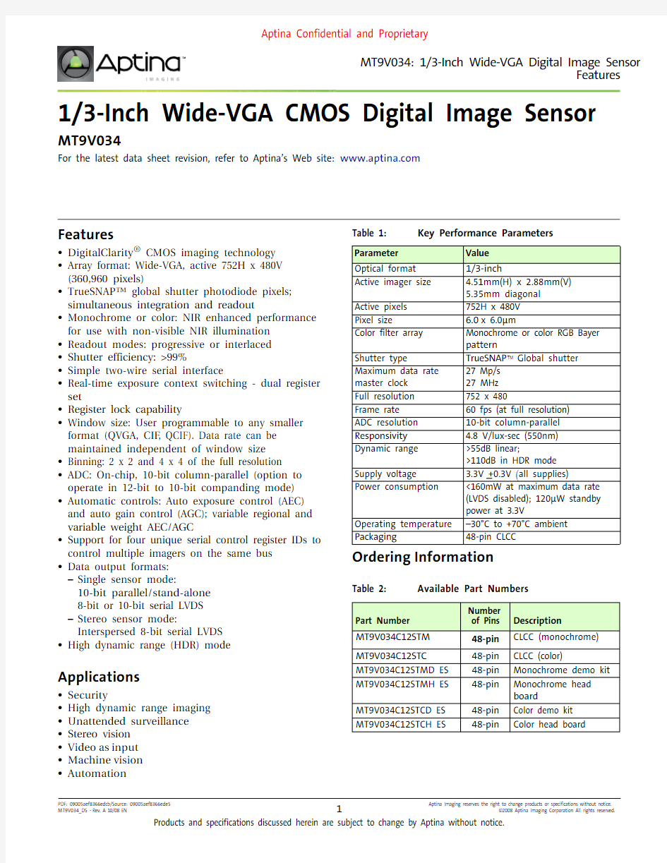
Table 1:
Key Performance Parameters
Ordering Information
Parameter
Value
Optical format 1/3-inch
Active imager size 4.51mm(H) x 2.88mm(V)5.35mm diagonal Active pixels 752H x 480V Pixel size
6.0x 6.0μm
Color filter array Monochrome or color RGB Bayer pattern
Shutter type
TrueSNAP ? Global shutter Maximum data rate master clock 27 Mp/s 27 MHz Full resolution 752 x 480
Frame rate 60 fps (at full resolution)ADC resolution 10-bit column-parallel Responsivity 4.8 V/lux-sec (550nm)Dynamic range >55dB linear;
>110dB in HDR mode Supply voltage
3.3V +0.3V (all supplies)
Power consumption
<160mW at maximum data rate (LVDS disabled); 120μW standby power at 3.3V
Operating temperature –30°C to +70°C ambient Packaging
48-pin CLCC
Table 2:
Available Part Numbers
Part Number Number
of Pins Description MT9V034C12STM 48-pin CLCC (monochrome)MT9V034C12STC
48-pin CLCC (color)
MT9V034C12STMD ES 48-pin Monochrome demo kit MT9V034C12STMH ES 48-pin Monochrome head board
MT9V034C12STCD ES 48-pin Color demo kit MT9V034C12STCH ES
48-pin
Color head board
Table of Contents
Features. . . . . . . . . . . . . . . . . . . . . . . . . . . . . . . . . . . . . . . . . . . . . . . . . . . . . . . . . . . . . . . . . . . . . . . . . . . . . . . . . . . . . . . . . . . . . .1 Applications . . . . . . . . . . . . . . . . . . . . . . . . . . . . . . . . . . . . . . . . . . . . . . . . . . . . . . . . . . . . . . . . . . . . . . . . . . . . . . . . . . . . . . . . . .1 Ordering Information. . . . . . . . . . . . . . . . . . . . . . . . . . . . . . . . . . . . . . . . . . . . . . . . . . . . . . . . . . . . . . . . . . . . . . . . . . . . . . . . . .1 General Description . . . . . . . . . . . . . . . . . . . . . . . . . . . . . . . . . . . . . . . . . . . . . . . . . . . . . . . . . . . . . . . . . . . . . . . . . . . . . . . . . . .6 Pin Descriptions . . . . . . . . . . . . . . . . . . . . . . . . . . . . . . . . . . . . . . . . . . . . . . . . . . . . . . . . . . . . . . . . . . . . . . . . . . . . . . . . . . . . . .8 Pixel Data Format . . . . . . . . . . . . . . . . . . . . . . . . . . . . . . . . . . . . . . . . . . . . . . . . . . . . . . . . . . . . . . . . . . . . . . . . . . . . . . . . . . . .10 Pixel Array Structure . . . . . . . . . . . . . . . . . . . . . . . . . . . . . . . . . . . . . . . . . . . . . . . . . . . . . . . . . . . . . . . . . . . . . . . . . . . . . . .10 Color Device Limitations. . . . . . . . . . . . . . . . . . . . . . . . . . . . . . . . . . . . . . . . . . . . . . . . . . . . . . . . . . . . . . . . . . . . . . . . . . . . . .11 Pixel Binning . . . . . . . . . . . . . . . . . . . . . . . . . . . . . . . . . . . . . . . . . . . . . . . . . . . . . . . . . . . . . . . . . . . . . . . . . . . . . . . . . . . . . .11 Interlaced Readout. . . . . . . . . . . . . . . . . . . . . . . . . . . . . . . . . . . . . . . . . . . . . . . . . . . . . . . . . . . . . . . . . . . . . . . . . . . . . . . . .11 Automatic Black Level Calibration. . . . . . . . . . . . . . . . . . . . . . . . . . . . . . . . . . . . . . . . . . . . . . . . . . . . . . . . . . . . . . . . . . .11 Other Limiting Factors . . . . . . . . . . . . . . . . . . . . . . . . . . . . . . . . . . . . . . . . . . . . . . . . . . . . . . . . . . . . . . . . . . . . . . . . . . . . .11 Output Data Format. . . . . . . . . . . . . . . . . . . . . . . . . . . . . . . . . . . . . . . . . . . . . . . . . . . . . . . . . . . . . . . . . . . . . . . . . . . . . . . . . .12 Output Data Timing. . . . . . . . . . . . . . . . . . . . . . . . . . . . . . . . . . . . . . . . . . . . . . . . . . . . . . . . . . . . . . . . . . . . . . . . . . . . . . . .13 Serial Bus Description . . . . . . . . . . . . . . . . . . . . . . . . . . . . . . . . . . . . . . . . . . . . . . . . . . . . . . . . . . . . . . . . . . . . . . . . . . . . . . . .15 Protocol . . . . . . . . . . . . . . . . . . . . . . . . . . . . . . . . . . . . . . . . . . . . . . . . . . . . . . . . . . . . . . . . . . . . . . . . . . . . . . . . . . . . . . . . . .15 Start Bit. . . . . . . . . . . . . . . . . . . . . . . . . . . . . . . . . . . . . . . . . . . . . . . . . . . . . . . . . . . . . . . . . . . . . . . . . . . . . . . . . . . . . . . . . . .15 Slave Address. . . . . . . . . . . . . . . . . . . . . . . . . . . . . . . . . . . . . . . . . . . . . . . . . . . . . . . . . . . . . . . . . . . . . . . . . . . . . . . . . . . . . .15 Acknowledge Bit. . . . . . . . . . . . . . . . . . . . . . . . . . . . . . . . . . . . . . . . . . . . . . . . . . . . . . . . . . . . . . . . . . . . . . . . . . . . . . . . . . .15 No-Acknowledge Bit . . . . . . . . . . . . . . . . . . . . . . . . . . . . . . . . . . . . . . . . . . . . . . . . . . . . . . . . . . . . . . . . . . . . . . . . . . . . . . .15 Stop Bit. . . . . . . . . . . . . . . . . . . . . . . . . . . . . . . . . . . . . . . . . . . . . . . . . . . . . . . . . . . . . . . . . . . . . . . . . . . . . . . . . . . . . . . . . . .15 Sequence . . . . . . . . . . . . . . . . . . . . . . . . . . . . . . . . . . . . . . . . . . . . . . . . . . . . . . . . . . . . . . . . . . . . . . . . . . . . . . . . . . . . . . . . .16 Bus Idle State. . . . . . . . . . . . . . . . . . . . . . . . . . . . . . . . . . . . . . . . . . . . . . . . . . . . . . . . . . . . . . . . . . . . . . . . . . . . . . . . . . . . . .16 Data Bit Transfer. . . . . . . . . . . . . . . . . . . . . . . . . . . . . . . . . . . . . . . . . . . . . . . . . . . . . . . . . . . . . . . . . . . . . . . . . . . . . . . . . . .16 Two-Wire Serial Interface Sample Read and Write Sequences. . . . . . . . . . . . . . . . . . . . . . . . . . . . . . . . . . . . . . . . . . . . .17 16-Bit Write Sequence. . . . . . . . . . . . . . . . . . . . . . . . . . . . . . . . . . . . . . . . . . . . . . . . . . . . . . . . . . . . . . . . . . . . . . . . . . . . . .17 16-Bit Read Sequence . . . . . . . . . . . . . . . . . . . . . . . . . . . . . . . . . . . . . . . . . . . . . . . . . . . . . . . . . . . . . . . . . . . . . . . . . . . . . .17 8-Bit Write Sequence. . . . . . . . . . . . . . . . . . . . . . . . . . . . . . . . . . . . . . . . . . . . . . . . . . . . . . . . . . . . . . . . . . . . . . . . . . . . . . .18 8-Bit Read Sequence . . . . . . . . . . . . . . . . . . . . . . . . . . . . . . . . . . . . . . . . . . . . . . . . . . . . . . . . . . . . . . . . . . . . . . . . . . . . . . .18 Register Lock. . . . . . . . . . . . . . . . . . . . . . . . . . . . . . . . . . . . . . . . . . . . . . . . . . . . . . . . . . . . . . . . . . . . . . . . . . . . . . . . . . . . . .19 Lock All Registers. . . . . . . . . . . . . . . . . . . . . . . . . . . . . . . . . . . . . . . . . . . . . . . . . . . . . . . . . . . . . . . . . . . . . . . . . . . . . . . .19 Lock Only Read Mode Registers (R0x0D and R0x0E). . . . . . . . . . . . . . . . . . . . . . . . . . . . . . . . . . . . . . . . . . . . . . . . .19 Real-Time Context Switching . . . . . . . . . . . . . . . . . . . . . . . . . . . . . . . . . . . . . . . . . . . . . . . . . . . . . . . . . . . . . . . . . . . . . . .20 Registers . . . . . . . . . . . . . . . . . . . . . . . . . . . . . . . . . . . . . . . . . . . . . . . . . . . . . . . . . . . . . . . . . . . . . . . . . . . . . . . . . . . . . . . . . . . .21 Shadowed Register. . . . . . . . . . . . . . . . . . . . . . . . . . . . . . . . . . . . . . . . . . . . . . . . . . . . . . . . . . . . . . . . . . . . . . . . . . . . . . . . .25 Feature Description . . . . . . . . . . . . . . . . . . . . . . . . . . . . . . . . . . . . . . . . . . . . . . . . . . . . . . . . . . . . . . . . . . . . . . . . . . . . . . . . . .47 Operational Modes . . . . . . . . . . . . . . . . . . . . . . . . . . . . . . . . . . . . . . . . . . . . . . . . . . . . . . . . . . . . . . . . . . . . . . . . . . . . . . . .47 Master Mode. . . . . . . . . . . . . . . . . . . . . . . . . . . . . . . . . . . . . . . . . . . . . . . . . . . . . . . . . . . . . . . . . . . . . . . . . . . . . . . . . . . .47 Simultaneous Master Mode . . . . . . . . . . . . . . . . . . . . . . . . . . . . . . . . . . . . . . . . . . . . . . . . . . . . . . . . . . . . . . . . . . . . . .47 Sequential Master Mode . . . . . . . . . . . . . . . . . . . . . . . . . . . . . . . . . . . . . . . . . . . . . . . . . . . . . . . . . . . . . . . . . . . . . . . . .48 Snapshot Mode . . . . . . . . . . . . . . . . . . . . . . . . . . . . . . . . . . . . . . . . . . . . . . . . . . . . . . . . . . . . . . . . . . . . . . . . . . . . . . . . .48 Slave Mode . . . . . . . . . . . . . . . . . . . . . . . . . . . . . . . . . . . . . . . . . . . . . . . . . . . . . . . . . . . . . . . . . . . . . . . . . . . . . . . . . . . . .49 Signal Path. . . . . . . . . . . . . . . . . . . . . . . . . . . . . . . . . . . . . . . . . . . . . . . . . . . . . . . . . . . . . . . . . . . . . . . . . . . . . . . . . . . . . . . .50 On-Chip Biases. . . . . . . . . . . . . . . . . . . . . . . . . . . . . . . . . . . . . . . . . . . . . . . . . . . . . . . . . . . . . . . . . . . . . . . . . . . . . . . . . . . .50 ADC Voltage Reference . . . . . . . . . . . . . . . . . . . . . . . . . . . . . . . . . . . . . . . . . . . . . . . . . . . . . . . . . . . . . . . . . . . . . . . . . .50 V_Step Voltage Reference . . . . . . . . . . . . . . . . . . . . . . . . . . . . . . . . . . . . . . . . . . . . . . . . . . . . . . . . . . . . . . . . . . . . . . . .51 Chip Version. . . . . . . . . . . . . . . . . . . . . . . . . . . . . . . . . . . . . . . . . . . . . . . . . . . . . . . . . . . . . . . . . . . . . . . . . . . . . . . . . . . .51 Window Control . . . . . . . . . . . . . . . . . . . . . . . . . . . . . . . . . . . . . . . . . . . . . . . . . . . . . . . . . . . . . . . . . . . . . . . . . . . . . . . . . . .51 Blanking Control. . . . . . . . . . . . . . . . . . . . . . . . . . . . . . . . . . . . . . . . . . . . . . . . . . . . . . . . . . . . . . . . . . . . . . . . . . . . . . . . . . .51 Pixel Integration Control . . . . . . . . . . . . . . . . . . . . . . . . . . . . . . . . . . . . . . . . . . . . . . . . . . . . . . . . . . . . . . . . . . . . . . . . . . .52 Total Integration . . . . . . . . . . . . . . . . . . . . . . . . . . . . . . . . . . . . . . . . . . . . . . . . . . . . . . . . . . . . . . . . . . . . . . . . . . . . . . . .52
Changes to Integration Time . . . . . . . . . . . . . . . . . . . . . . . . . . . . . . . . . . . . . . . . . . . . . . . . . . . . . . . . . . . . . . . . . . . . .53 Exposure Indicator . . . . . . . . . . . . . . . . . . . . . . . . . . . . . . . . . . . . . . . . . . . . . . . . . . . . . . . . . . . . . . . . . . . . . . . . . . . . . .54 High Dynamic Range . . . . . . . . . . . . . . . . . . . . . . . . . . . . . . . . . . . . . . . . . . . . . . . . . . . . . . . . . . . . . . . . . . . . . . . . . . . .54 ADC Companding Mode. . . . . . . . . . . . . . . . . . . . . . . . . . . . . . . . . . . . . . . . . . . . . . . . . . . . . . . . . . . . . . . . . . . . . . . . . . . .56 Gain Settings . . . . . . . . . . . . . . . . . . . . . . . . . . . . . . . . . . . . . . . . . . . . . . . . . . . . . . . . . . . . . . . . . . . . . . . . . . . . . . . . . . . . . .57 Changes to Gain Settings. . . . . . . . . . . . . . . . . . . . . . . . . . . . . . . . . . . . . . . . . . . . . . . . . . . . . . . . . . . . . . . . . . . . . . . . .57 Analog Gain . . . . . . . . . . . . . . . . . . . . . . . . . . . . . . . . . . . . . . . . . . . . . . . . . . . . . . . . . . . . . . . . . . . . . . . . . . . . . . . . . . . .58 Digital Gain. . . . . . . . . . . . . . . . . . . . . . . . . . . . . . . . . . . . . . . . . . . . . . . . . . . . . . . . . . . . . . . . . . . . . . . . . . . . . . . . . . . . .58 Black Level Calibration . . . . . . . . . . . . . . . . . . . . . . . . . . . . . . . . . . . . . . . . . . . . . . . . . . . . . . . . . . . . . . . . . . . . . . . . . . . . .59 Row-wise Noise Correction . . . . . . . . . . . . . . . . . . . . . . . . . . . . . . . . . . . . . . . . . . . . . . . . . . . . . . . . . . . . . . . . . . . . . . . . .61 Automatic Gain Control and Automatic Exposure Control . . . . . . . . . . . . . . . . . . . . . . . . . . . . . . . . . . . . . . . . . . . . .61 Pixel Clock Speed . . . . . . . . . . . . . . . . . . . . . . . . . . . . . . . . . . . . . . . . . . . . . . . . . . . . . . . . . . . . . . . . . . . . . . . . . . . . . . . . . .62 Hard Reset of Logic . . . . . . . . . . . . . . . . . . . . . . . . . . . . . . . . . . . . . . . . . . . . . . . . . . . . . . . . . . . . . . . . . . . . . . . . . . . . . . . .63 Soft Reset of Logic . . . . . . . . . . . . . . . . . . . . . . . . . . . . . . . . . . . . . . . . . . . . . . . . . . . . . . . . . . . . . . . . . . . . . . . . . . . . . . . . .63 STANDBY Control . . . . . . . . . . . . . . . . . . . . . . . . . . . . . . . . . . . . . . . . . . . . . . . . . . . . . . . . . . . . . . . . . . . . . . . . . . . . . . . . .63 Monitor Mode Control . . . . . . . . . . . . . . . . . . . . . . . . . . . . . . . . . . . . . . . . . . . . . . . . . . . . . . . . . . . . . . . . . . . . . . . . . . . . .63 Read Mode Options. . . . . . . . . . . . . . . . . . . . . . . . . . . . . . . . . . . . . . . . . . . . . . . . . . . . . . . . . . . . . . . . . . . . . . . . . . . . . . . .63 Column Flip . . . . . . . . . . . . . . . . . . . . . . . . . . . . . . . . . . . . . . . . . . . . . . . . . . . . . . . . . . . . . . . . . . . . . . . . . . . . . . . . . . . .63 Row Flip. . . . . . . . . . . . . . . . . . . . . . . . . . . . . . . . . . . . . . . . . . . . . . . . . . . . . . . . . . . . . . . . . . . . . . . . . . . . . . . . . . . . . . . .64 Pixel Binning. . . . . . . . . . . . . . . . . . . . . . . . . . . . . . . . . . . . . . . . . . . . . . . . . . . . . . . . . . . . . . . . . . . . . . . . . . . . . . . . . . . .64 Row Binning. . . . . . . . . . . . . . . . . . . . . . . . . . . . . . . . . . . . . . . . . . . . . . . . . . . . . . . . . . . . . . . . . . . . . . . . . . . . . . . . . . . .65 Column Binning . . . . . . . . . . . . . . . . . . . . . . . . . . . . . . . . . . . . . . . . . . . . . . . . . . . . . . . . . . . . . . . . . . . . . . . . . . . . . . . .65 Interlaced Readout . . . . . . . . . . . . . . . . . . . . . . . . . . . . . . . . . . . . . . . . . . . . . . . . . . . . . . . . . . . . . . . . . . . . . . . . . . . . . .66 LINE_VALID . . . . . . . . . . . . . . . . . . . . . . . . . . . . . . . . . . . . . . . . . . . . . . . . . . . . . . . . . . . . . . . . . . . . . . . . . . . . . . . . . . . . . .68 LVDS Serial (Stand-Alone/Stereo) Output . . . . . . . . . . . . . . . . . . . . . . . . . . . . . . . . . . . . . . . . . . . . . . . . . . . . . . . . . . . .68 LVDS Output Format. . . . . . . . . . . . . . . . . . . . . . . . . . . . . . . . . . . . . . . . . . . . . . . . . . . . . . . . . . . . . . . . . . . . . . . . . . . . . . .69 LVDS Enable and Disable. . . . . . . . . . . . . . . . . . . . . . . . . . . . . . . . . . . . . . . . . . . . . . . . . . . . . . . . . . . . . . . . . . . . . . . . . . .71 LVDS Data Bus Timing . . . . . . . . . . . . . . . . . . . . . . . . . . . . . . . . . . . . . . . . . . . . . . . . . . . . . . . . . . . . . . . . . . . . . . . . . . . . .72 Electrical Specifications. . . . . . . . . . . . . . . . . . . . . . . . . . . . . . . . . . . . . . . . . . . . . . . . . . . . . . . . . . . . . . . . . . . . . . . . . . . . . . .73 Propagation Delays for PIXCLK and Data Out Signals. . . . . . . . . . . . . . . . . . . . . . . . . . . . . . . . . . . . . . . . . . . . . . . . . .75 Propagation Delays for FRAME_VALID and LINE_VALID Signals . . . . . . . . . . . . . . . . . . . . . . . . . . . . . . . . . . . . . . .75 Two-Wire Serial Bus Timing . . . . . . . . . . . . . . . . . . . . . . . . . . . . . . . . . . . . . . . . . . . . . . . . . . . . . . . . . . . . . . . . . . . . . . . .76 Minimum Master Clock Cycles . . . . . . . . . . . . . . . . . . . . . . . . . . . . . . . . . . . . . . . . . . . . . . . . . . . . . . . . . . . . . . . . . . .77 Package Dimensions . . . . . . . . . . . . . . . . . . . . . . . . . . . . . . . . . . . . . . . . . . . . . . . . . . . . . . . . . . . . . . . . . . . . . . . . . . . . . . . . .80 Appendix A–Power-On Reset and Standby Timing . . . . . . . . . . . . . . . . . . . . . . . . . . . . . . . . . . . . . . . . . . . . . . . . . . . . . .81 Revision History. . . . . . . . . . . . . . . . . . . . . . . . . . . . . . . . . . . . . . . . . . . . . . . . . . . . . . . . . . . . . . . . . . . . . . . . . . . . . . . . . . . . . .82
List of Figures
Figure 1:Block Diagram. . . . . . . . . . . . . . . . . . . . . . . . . . . . . . . . . . . . . . . . . . . . . . . . . . . . . . . . . . . . . . . . . . . . . . . . . . . .6 Figure 2:48-Pin CLCC Package Pinout Diagram . . . . . . . . . . . . . . . . . . . . . . . . . . . . . . . . . . . . . . . . . . . . . . . . . . . . . .7 Figure 3:Typical Configuration (Connection)—Parallel Output Mode. . . . . . . . . . . . . . . . . . . . . . . . . . . . . . . . . . .9 Figure 4:Pixel Array Description . . . . . . . . . . . . . . . . . . . . . . . . . . . . . . . . . . . . . . . . . . . . . . . . . . . . . . . . . . . . . . . . . . .10 Figure 5:Pixel Color Pattern Detail (Top Right Corner) . . . . . . . . . . . . . . . . . . . . . . . . . . . . . . . . . . . . . . . . . . . . . . .11 Figure 6:Spatial Illustration of Image Readout. . . . . . . . . . . . . . . . . . . . . . . . . . . . . . . . . . . . . . . . . . . . . . . . . . . . . . .12 Figure 7:Timing Example of Pixel Data . . . . . . . . . . . . . . . . . . . . . . . . . . . . . . . . . . . . . . . . . . . . . . . . . . . . . . . . . . . . .13 Figure 8:Row Timing and FRAME_VALID/LINE_VALID Signals . . . . . . . . . . . . . . . . . . . . . . . . . . . . . . . . . . . . . . .13 Figure 9:Timing Diagram Showing a Write to R0x09 with the Value 0x0284. . . . . . . . . . . . . . . . . . . . . . . . . . . . .17 Figure 10:Timing Diagram Showing a Read from R0x09; Returned Value 0x0284 . . . . . . . . . . . . . . . . . . . . . . . . .17 Figure 11:Timing Diagram Showing a Bytewise Write to R0x09 with the Value 0x0284 . . . . . . . . . . . . . . . . . . . .18 Figure 12:Timing Diagram Showing a Bytewise Read from R0x09; Returned Value 0x0284 . . . . . . . . . . . . . . . .18 Figure 13:Simultaneous Master Mode Synchronization Waveforms #1. . . . . . . . . . . . . . . . . . . . . . . . . . . . . . . . . .47 Figure 14:Simultaneous Master Mode Synchronization Waveforms #2. . . . . . . . . . . . . . . . . . . . . . . . . . . . . . . . . .48 Figure 15:Sequential Master Mode Synchronization Waveforms . . . . . . . . . . . . . . . . . . . . . . . . . . . . . . . . . . . . . . .48 Figure 16:Snapshot Mode Interface Signals . . . . . . . . . . . . . . . . . . . . . . . . . . . . . . . . . . . . . . . . . . . . . . . . . . . . . . . . . .49 Figure 17:Snapshot Mode Frame Synchronization Waveforms. . . . . . . . . . . . . . . . . . . . . . . . . . . . . . . . . . . . . . . . .49 Figure 18:Slave Mode Operation. . . . . . . . . . . . . . . . . . . . . . . . . . . . . . . . . . . . . . . . . . . . . . . . . . . . . . . . . . . . . . . . . . . .50 Figure 19:Signal Path . . . . . . . . . . . . . . . . . . . . . . . . . . . . . . . . . . . . . . . . . . . . . . . . . . . . . . . . . . . . . . . . . . . . . . . . . . . . . .50 Figure 20:Latency When Changing Integration . . . . . . . . . . . . . . . . . . . . . . . . . . . . . . . . . . . . . . . . . . . . . . . . . . . . . . .53 Figure 21:Sequence of Control Voltages at the HDR Gate. . . . . . . . . . . . . . . . . . . . . . . . . . . . . . . . . . . . . . . . . . . . . .54 Figure 22:Sequence of Voltages in a Piecewise Linear Pixel Response . . . . . . . . . . . . . . . . . . . . . . . . . . . . . . . . . . .55 Figure 23:12- to 10-Bit Companding Chart. . . . . . . . . . . . . . . . . . . . . . . . . . . . . . . . . . . . . . . . . . . . . . . . . . . . . . . . . . .56 Figure 24:Latency of Analog Gain Change When AGC Is Disabled . . . . . . . . . . . . . . . . . . . . . . . . . . . . . . . . . . . . . .57 Figure 25:Tiled Sample . . . . . . . . . . . . . . . . . . . . . . . . . . . . . . . . . . . . . . . . . . . . . . . . . . . . . . . . . . . . . . . . . . . . . . . . . . . .59 Figure 26:Black Level Calibration Flow Chart. . . . . . . . . . . . . . . . . . . . . . . . . . . . . . . . . . . . . . . . . . . . . . . . . . . . . . . . .59 Figure 27:Controllable and Observable AEC/AGC Registers. . . . . . . . . . . . . . . . . . . . . . . . . . . . . . . . . . . . . . . . . . . .62 Figure 28:Readout of Six Pixels in Normal and Column Flip Output Mode. . . . . . . . . . . . . . . . . . . . . . . . . . . . . . .64 Figure 29:Readout of Six Rows in Normal and Row Flip Output Mode . . . . . . . . . . . . . . . . . . . . . . . . . . . . . . . . . .64 Figure 30:Readout of 8 Pixels in Normal and Row Bin Output Mode . . . . . . . . . . . . . . . . . . . . . . . . . . . . . . . . . . . .65 Figure 31:Readout of 8 Pixels in Normal and Column Bin Output Mode. . . . . . . . . . . . . . . . . . . . . . . . . . . . . . . . .66 Figure 32:Spatial Illustration of Interlaced Image Readout. . . . . . . . . . . . . . . . . . . . . . . . . . . . . . . . . . . . . . . . . . . . .67 Figure 33:Different LINE_VALID Formats. . . . . . . . . . . . . . . . . . . . . . . . . . . . . . . . . . . . . . . . . . . . . . . . . . . . . . . . . . . .68 Figure 34:Serial Output Format for a 6x2 Frame . . . . . . . . . . . . . . . . . . . . . . . . . . . . . . . . . . . . . . . . . . . . . . . . . . . . . .69 Figure 35:LVDS Timing . . . . . . . . . . . . . . . . . . . . . . . . . . . . . . . . . . . . . . . . . . . . . . . . . . . . . . . . . . . . . . . . . . . . . . . . . . . .72 Figure 36:Propagation Delays for PIXCLK and Data Out Signals. . . . . . . . . . . . . . . . . . . . . . . . . . . . . . . . . . . . . . . .75 Figure 37:Propagation Delays for FRAME_VALID and LINE_VALID Signals. . . . . . . . . . . . . . . . . . . . . . . . . . . . . .75 Figure 38:Two-wire Serial Bus Timing . . . . . . . . . . . . . . . . . . . . . . . . . . . . . . . . . . . . . . . . . . . . . . . . . . . . . . . . . . . . . . .76 Figure 39:Serial Host Interface Start Condition Timing. . . . . . . . . . . . . . . . . . . . . . . . . . . . . . . . . . . . . . . . . . . . . . . .77 Figure 40:Serial Host Interface Stop Condition Timing . . . . . . . . . . . . . . . . . . . . . . . . . . . . . . . . . . . . . . . . . . . . . . . .77 Figure 41:Serial Host Interface Data Timing for Write . . . . . . . . . . . . . . . . . . . . . . . . . . . . . . . . . . . . . . . . . . . . . . . . .77 Figure 42:Serial Host Interface Data Timing for Read . . . . . . . . . . . . . . . . . . . . . . . . . . . . . . . . . . . . . . . . . . . . . . . . .78 Figure 43:Acknowledge Signal Timing After an 8-Bit WRITE to the Sensor. . . . . . . . . . . . . . . . . . . . . . . . . . . . . . .78 Figure 44:Acknowledge Signal Timing After an 8-Bit READ from the Sensor . . . . . . . . . . . . . . . . . . . . . . . . . . . . .78 Figure 45:Typical Quantum Efficiency – Color. . . . . . . . . . . . . . . . . . . . . . . . . . . . . . . . . . . . . . . . . . . . . . . . . . . . . . . .79 Figure 46:Typical Quantum Efficiency – Monochrome . . . . . . . . . . . . . . . . . . . . . . . . . . . . . . . . . . . . . . . . . . . . . . . .79 Figure 47:48-Pin CLCC Package Outline Drawing. . . . . . . . . . . . . . . . . . . . . . . . . . . . . . . . . . . . . . . . . . . . . . . . . . . . .80 Figure 48:Power-up, Reset, Clock and Standby Sequence. . . . . . . . . . . . . . . . . . . . . . . . . . . . . . . . . . . . . . . . . . . . . .81
List of Tables
Table 1:Key Performance Parameters. . . . . . . . . . . . . . . . . . . . . . . . . . . . . . . . . . . . . . . . . . . . . . . . . . . . . . . . . . . . . . .1 Table 2:Available Part Numbers. . . . . . . . . . . . . . . . . . . . . . . . . . . . . . . . . . . . . . . . . . . . . . . . . . . . . . . . . . . . . . . . . . . .1 Table 3:Pin Descriptions . . . . . . . . . . . . . . . . . . . . . . . . . . . . . . . . . . . . . . . . . . . . . . . . . . . . . . . . . . . . . . . . . . . . . . . . . .8 Table 4:Frame Time . . . . . . . . . . . . . . . . . . . . . . . . . . . . . . . . . . . . . . . . . . . . . . . . . . . . . . . . . . . . . . . . . . . . . . . . . . . . .13 Table 5:Frame Time—Long Integration Time . . . . . . . . . . . . . . . . . . . . . . . . . . . . . . . . . . . . . . . . . . . . . . . . . . . . . .14 Table 6:Slave Address Modes . . . . . . . . . . . . . . . . . . . . . . . . . . . . . . . . . . . . . . . . . . . . . . . . . . . . . . . . . . . . . . . . . . . . .16 Table 7:Real-Time Context-Switchable Registers . . . . . . . . . . . . . . . . . . . . . . . . . . . . . . . . . . . . . . . . . . . . . . . . . . .20 Table 8:Default Register Descriptions . . . . . . . . . . . . . . . . . . . . . . . . . . . . . . . . . . . . . . . . . . . . . . . . . . . . . . . . . . . . .21 Table 9:Register Descriptions. . . . . . . . . . . . . . . . . . . . . . . . . . . . . . . . . . . . . . . . . . . . . . . . . . . . . . . . . . . . . . . . . . . . .25 Table 10:LVDS Packet Format in Stand-Alone Mode . . . . . . . . . . . . . . . . . . . . . . . . . . . . . . . . . . . . . . . . . . . . . . . . .69 Table 11:LVDS Packet Format in Stereoscopy Mode (Stereoscopy Mode Bit Asserted) . . . . . . . . . . . . . . . . . . .70 Table 12:Reserved Words in the Pixel Data Stream . . . . . . . . . . . . . . . . . . . . . . . . . . . . . . . . . . . . . . . . . . . . . . . . . . .70 Table 13:SER_DATAOUT_* state . . . . . . . . . . . . . . . . . . . . . . . . . . . . . . . . . . . . . . . . . . . . . . . . . . . . . . . . . . . . . . . . . . .71 Table 14:SHFT_CLK_* state. . . . . . . . . . . . . . . . . . . . . . . . . . . . . . . . . . . . . . . . . . . . . . . . . . . . . . . . . . . . . . . . . . . . . . . .71 Table 15:LVDS AC Timing Specifications. . . . . . . . . . . . . . . . . . . . . . . . . . . . . . . . . . . . . . . . . . . . . . . . . . . . . . . . . . . .72 Table 16:DC Electrical Characteristics Over Temperature. . . . . . . . . . . . . . . . . . . . . . . . . . . . . . . . . . . . . . . . . . . . .73 Table 17:DC Electrical Characteristics . . . . . . . . . . . . . . . . . . . . . . . . . . . . . . . . . . . . . . . . . . . . . . . . . . . . . . . . . . . . . .73 Table 18:Absolute Maximum Ratings. . . . . . . . . . . . . . . . . . . . . . . . . . . . . . . . . . . . . . . . . . . . . . . . . . . . . . . . . . . . . . .74 Table 19:AC Electrical Characteristics . . . . . . . . . . . . . . . . . . . . . . . . . . . . . . . . . . . . . . . . . . . . . . . . . . . . . . . . . . . . . .74 Table 20:Two-Wire Serial Bus Timing Parameters. . . . . . . . . . . . . . . . . . . . . . . . . . . . . . . . . . . . . . . . . . . . . . . . . . . .76
General Description
The MT9V034 is a 1/3-inch wide-VGA format CMOS active-pixel digital image sensor with TrueSNAP? global shutter and high dynamic range (HDR) operation. The sensor has specifically been designed to support the demanding interior and exterior surveil-lance imaging needs, which makes this part ideal for a wide variety of imaging applica-tions in real-world environments.
This wide-VGA CMOS image sensor features DigitalClarity ?Aptina’s breakthrough low-noise CMOS imaging technology that achieves CCD image quality (based on
signal-to-noise ratio and low-light sensitivity) while maintaining the inherent size, cost, and integration advantages of CMOS.
The active imaging pixel array is 752H x 480V . It incorporates sophisticated camera func-tions on-chip—such as binning 2x 2 and 4x 4, to improve sensitivity when operating in smaller resolutions—as well as windowing, column and row mirroring. It is program-mable through a simple two-wire serial interface.
The MT9V034 can be operated in its default mode or be programmed for frame size, exposure, gain setting, and other parameters. The default mode outputs a wide-VGA-size image at 60 frames per second (fps).
An on-chip analog-to-digital converter (ADC) provides 10 bits per pixel. A 12-bit resolu-tion companded for 10 bits for small signals can be alternatively enabled, allowing more accurate digitization for darker areas in the image.
In addition to a traditional, parallel logic output the MT9V034 also features a serial low-voltage differential signaling (LVDS) output. The sensor can be operated in a stereo-camera, and the sensor, designated as a stereo-master, is able to merge the data from itself and the stereo-slave sensor into one serial LVDS stream.
The sensor is designed to operate in a wide temperature range (–30°C to +70°C).
Figure 1: Block Diagram
Pin Descriptions
Table 3: Pin Descriptions
48-Pin CLCC
Numbers Symbol Type Description Note
D GND.1
29RSVD Input Connect
to
10SER_DATAIN_N Input Serial data in for stereoscopy (differential negative). Tie to 1KΩ
pull-up (to 3.3V) in non-stereoscopy mode.
11SER_DATAIN_P Input Serial data in for stereoscopy (differential positive). Tie to D GND in
non-stereoscopy mode.
8BYPASS_CLKIN_N Input Input bypass shift-CLK (differential negative). Tie to 1KΩ pull-up
(to 3.3V) in non-stereoscopy mode.
9BYPASS_CLKIN_P Input Input bypass shift-CLK (differential positive). Tie to D GND in non-
stereoscopy mode.
23EXPOSURE Input Rising edge starts exposure in snapshot and slave modes.
25SCLK Input Two-wire serial interface clock. Connect to V DD with 1.5K resistor
even when no other two-wire serial interface peripheral is
attached.
28OE Input D OUT enable pad, active HIGH.2 30S_CTRL_ADR0Input Two-wire serial interface slave address select (see Table6 on
page16).
31S_CTRL_ADR1Input Two-wire serial interface slave address select (see Table6 on
page16).
32RESET_BAR Input Asynchronous reset. All registers assume defaults.
33STANDBY Input Shut down sensor operation for power saving.
47SYSCLK Input Master clock (26.6 MHz; 13MHz – 27MHz).
24S DATA I/O Two-wire serial interface data. Connect to V DD with 1.5K resistor
even when no other two-wire serial interface peripheral is
attached.
22STLN_OUT I/O Output in master mode—start line sync to drive slave chip in-
phase; input in slave mode.
26STFRM_OUT I/O Output in master mode—start frame sync to drive a slave chip in-
phase; input in slave mode.
20LINE_VALID Output Asserted when D OUT data is valid.
21FRAME_VALID Output Asserted when D OUT data is valid.
15D OUT5Output Parallel pixel data output 5.
16D OUT6Output Parallel pixel data output 6.
17D OUT7Output Parallel pixel data output 7.
18D OUT8Output Parallel pixel data output 8.
19D OUT9Output Parallel pixel data output 9.
27LED_OUT Output LED strobe output.
41D OUT4Output Parallel pixel data output 4.
42D OUT3Output Parallel pixel data output 3.
43D OUT2Output Parallel pixel data output 2.
44D OUT1Output Parallel pixel data output 1.
45D OUT0Output Parallel pixel data output 0.
46PIXCLK Output Pixel clock out. D OUT is valid on rising edge of this clock.
2SHFT_CLKOUT_N Output Output shift CLK (differential negative).
3SHFT_CLKOUT_P Output Output shift CLK (differential positive).
4SER_DATAOUT_N Output Serial data out (differential negative).
Notes:
1.Pin 29, (RSVD) must be tied to GND.
2.Output enable (OE) tri-states signals D OUT 0–D OUT 9, LINE_VALID, FRAME_VALID, and PIXCLK.
3.No connect. These pins must be left floating for proper operation.
Figure 3: Typical Configuration (Connection)—Parallel Output Mode
Note:LVDS signals are to be left floating.
5SER_DATAOUT_P
Output Serial data out (differential positive).1,14V DD Supply Digital power 3.3V.35,39V AA Supply Analog power 3.3V.40VAAPIX Supply Pixel power 3.3V.
6V DD LVDS Supply Dedicated power for LVDS pads.7,12LVDSGND Ground Dedicated GND for LVDS pads.13,48D GND Ground Digital GND.34,38A GND Ground Analog GND.36,37
NC NC
No connect.
3
Table 3:
Pin Descriptions (continued)
48-Pin CLCC Numbers
Symbol Type Description
Note
Pixel Data Format
Pixel Array Structure
The MT9V034 pixel array is configured as 809 columns by 499 rows, shown in Figure4.
The dark pixels are optically black and are used internally to monitor black level. Of the
left 52 columns, 36 are dark pixels used for row noise correction. Of the top 14 rows of
pixels, two of the dark rows are used for black level correction. Also, three black rows
from the top black rows can be read out by setting the Show Dark Rows bit in the Read
Mode register; setting Show Dark Columns will display the 36 dark columns. There are
753 columns by 481 rows of optically active pixels. While the sensor's format is 752 x 480,
one additional active column and active row are included for use when horizontal or
vertical mirrored readout is enabled, to allow readout to start on the same pixel. This one
pixel adjustment is always performed, for monochrome or color versions. The active
area is surrounded with optically transparent dummy pixels to improve image unifor-
mity within the active area. Neither dummy pixels nor barrier pixels can be read out. Figure 4: Pixel Array Description
Color Device Limitations
The color version of the MT9V034 does not support or offers reduced performance for
the following functionalities.
Pixel Binning
Pixel binning is done on immediate neighbor pixels only, no facility is provided to skip
pixels according to a Bayer pattern. Therefore, the result of binning combines pixels of
different colors. See “Pixel Binning” on page64 for additional information. Interlaced Readout
Interlaced readout yields one field consisting only of red and green pixels and another
consisting only of blue and green pixels. This is due to the Bayer pattern of the CFA. Automatic Black Level Calibration
When the color bit is set (R0x0F[1]=1), the sensor uses black level correction values from
one green plane, which are applied to all colors. To use the calibration value based on all
dark pixels' offset values, the color bit should be cleared.
Other Limiting Factors
Black level correction and row-wise noise correction are applied uniformly to each color.
The row-wise noise correction algorithm does not work well in color sensors. Automatic
exposure and gain control calculations are made based on all three colors, not just the
green channel. High dynamic range does operate in color; however, Aptina strongly
recommends limiting use to linear operation where good color fidelity is required.
Output Data Format
The MT9V034 image data can be read out in a progressive scan or interlaced scan mode.
Valid image data is surrounded by horizontal and vertical blanking, as shown in Figure6.
The amount of horizontal and vertical blanking is programmable through R0x05 and
R0x06, respectively (R0xCD and R0xCE for context B). LV is HIGH during the shaded
region of the figure. See “Output Data Timing” on page13 for the description of FV
timing.
Figure 6: Spatial Illustration of Image Readout
The PIXCLK is a nominally inverted version of the master clock (SYSCLK). This allows PIXCLK to be used as a clock to latch the data. However, when column bin 2 is enabled, the PIXCLK is HIGH for one complete master clock master period and then LOW for one complete master clock period; when column bin 4 is enabled, the PIXCLK is HIGH for two complete master clock periods and then LOW for two complete master clock periods. It is continuously enabled, even during the blanking period. Setting R0x72 bit[4]=1 causes the MT9V034 to invert the polarity of the PIXCLK.The parameters P1, A, Q, and P2 in Figure 8 are defined in Table 4.
Figure 8: Row Timing and FRAME_VALID/LINE_VALID Signals
Table 4: Frame Time
Parameter
Name
Equation Default Timing at 26.66 MHz A
Active data time
Context A: R0x04 Context B: R0xCC 752 pixel clocks = 752 master = 28.20μs P1Frame start blanking
Context A: R0x05 - 23Context B: R0xCD - 2371 pixel clocks = 71master = 2.66μs
P2Frame end blanking
23 (fixed)
23 pixel clocks = 23 master = 0.86μs
Q Horizontal blanking
Context A: R0x05Context B: R0xCD
94 pixel clocks = 94 master = 3.52μs
Sensor timing is shown above in terms of pixel clock and master clock cycles (refer to Figure 7 on page 13). The recommended master clock frequency is 26.66 MHz. The vertical blanking and the total frame time equations assume that the integration time (Coarse Shutter Width plus Fine Shutter Width) is less than the number of active rows plus the blanking rows minus the overhead rows:
Window Height + Vertical Blanking – 2
(EQ 1)
If this is not the case, the number of integration rows must be used instead to determine the frame time, as shown in Table 5. In this example it is assumed that the Coarse Shutter Width Control is programmed with 523 rows, and the Fine Shutter Width Total is zero. For Simultaneous mode, if the exposure time registers (Coarse Shutter Width Total plus Fine Shutter Width Total) exceed the total readout time, then the vertical blanking time is internally extended automatically to adjust for the additional integration time
required. This extended value is not written back to the vertical blanking registers. The Vertical Blank register can be used to adjust frame-to-frame readout time. This register does not affect the exposure time but it may extend the readout time.
Notes:
1.The MT9V034 uses column parallel analog-digital converters, thus short row timing is not possible. The minimum total row time is 690 columns (horizontal width + horizontal blanking). The mini-mum horizontal blanking is 61. When the window width is set below 627, horizontal blanking must be increased.
A+Q
Row time
Context A: R0x04 + R0x05Context B: R0xCC + R0xCD 846 pixel clocks = 846 master = 31.72μs
V Vertical blanking
Context A: (R0x06) x (A + Q) + 4Context B: (R0xCE) x (A + Q) + 438,074 pixel clocks = 38,074 master = 1.43ms
Nrows x (A + Q)Frame valid time
Context A: (R0x03) × (A + Q)Context B: (R0xCB) x (A + Q)406,080 pixel clocks = 406,080 master = 15.23ms
F Total frame time
V + (Nrows x (A + Q))
444,154 pixel clocks = 444,154 master = 16.66ms
Table 5:
Frame Time—Long Integration Time
Parameter
Name
Equation
(Number of Master Clock Cycles)
Default Timing at 26.66 MHz V’
Vertical blanking (long integration time)Context A: (R0x0B + 2 - R0x03) × (A + Q) + R0xD5 + 4Context B: (R0xD2 + 2 - R0xCB) x (A + Q) + R0xD8 + 438,074 pixel clocks = 38,074 master = 1.43ms
F
Total frame time (long integration time)
Context A: (R0x0B + 2) × (A + Q) + R0xD5 + 4Context B: (R0xD2 + 2) x (A + Q) + R0xD8 + 4
444,154 pixel clocks = 444,154 master = 16.66ms
Table 4:
Frame Time (continued)
Parameter Name Equation
Default Timing at 26.66 MHz
Serial Bus Description
Registers are written to and read from the MT9V034 through the two-wire serial inter-
face bus. The MT9V034 is a serial interface slave with four possible IDs (0x90, 0x98, 0xB0
and 0xB8) determined by the S_CTRL_ADR0 and S_CTRL_ADR1 input pins. Data is
transferred into the MT9V034 and out through the serial data (S DATA) line. The S DATA
line is pulled up to V DD off-chip by a 1.5KΩ resistor. Either the slave or master device can
pull the S DATA line down—the serial interface protocol determines which device is
allowed to pull the S DATA line down at any given time. The registers are 16-bit wide, and
can be accessed through 16- or 8-bit two-wire serial interface sequences.
Protocol
The two-wire serial interface defines several different transmission codes, as shown in
the following sequence:
1.a start bit
2.the slave device 8-bit address
3.a(n) (no) acknowledge bit
4.an 8-bit message
5.a stop bit
Start Bit
The start bit is defined as a HIGH-to-LOW transition of the data line while the clock line
is HIGH.
Slave Address
The 8-bit address of a two-wire serial interface device consists of 7 bits of address and
1bit of direction. A “0” in the LSB of the address indicates write mode, and a “1” indi-
cates read mode. As indicated above, the MT9V034 allows four possible slave addresses
determined by the two input pins, S_CTRL_ADR0 and S_CTRL_ADR1. Acknowledge Bit
The master generates the acknowledge clock pulse. The transmitter (which is the master
when writing, or the slave when reading) releases the data line, and the receiver indi-
cates an acknowledge bit by pulling the data line LOW during the acknowledge clock
pulse.
No-Acknowledge Bit
The no-acknowledge bit is generated when the data line is not pulled down by the
receiver during the acknowledge clock pulse. A no-acknowledge bit is used to terminate
a read sequence.
Stop Bit
The stop bit is defined as a LOW-to-HIGH transition of the data line while the clock line
is HIGH.
Sequence
A typical READ or WRITE sequence begins by the master sending a start bit. After the
start bit, the master sends the slave device’s 8-bit address. The last bit of the address
determines if the request is a read or a write, where a “0” indicates a WRITE and a “1”
indicates a READ. The slave device acknowledges its address by sending an acknowledge
bit back to the master.
If the request was a WRITE, the master then transfers the 8-bit register address to which
a WRITE should take place. The slave sends an acknowledge bit to indicate that the
register address has been received. The master then transfers the data 8 bits at a time,
with the slave sending an acknowledge bit after each 8 bits. The MT9V034 uses 16-bit
data for its internal registers, thus requiring two 8-bit transfers to write to one register.
After 16 bits are transferred, the register address is automatically incremented, so that
the next 16 bits are written to the next register address. The master stops writing by
sending a start or stop bit.
A typical READ sequence is executed as follows. First the master sends the write mode
slave address and 8-bit register address, just as in the write request. The master then
sends a start bit and the read mode slave address. The master then clocks out the register
data 8 bits at a time. The master sends an acknowledge bit after each 8-bit transfer. The
register address is automatically incremented after every 16 bits is transferred. The data
transfer is stopped when the master sends a no-acknowledge bit. The MT9V034 allows
for 8-bit data transfers through the two-wire serial interface by writing (or reading) the
most significant 8 bits to the register and then writing (or reading) the least significant 8
bits to Byte-Wise Address register (0x0F0).
Bus Idle State
The bus is idle when both the data and clock lines are HIGH. Control of the bus is initi-
ated with a start bit, and the bus is released with a stop bit. Only the master can generate
the start and stop bits.
Table 6: Slave Address Modes
{S_CTRL_ADR1, S_CTRL_ADR0}Slave Address Write/Read Mode
000x90Write
0x91Read
010x98Write
0x99Read
100xB0Write
0xB1Read
110xB8Write
0xB9Read
Data Bit Transfer
One data bit is transferred during each clock pulse. The two-wire serial interface clock
pulse is provided by the master. The data must be stable during the HIGH period of the
serial clock—it can only change when the two-wire serial interface clock is LOW. Data is
transferred 8 bits at a time, followed by an acknowledge bit.
Two-Wire Serial Interface Sample Read and Write Sequences
16-Bit Write Sequence
A typical write sequence for writing 16 bits to a register is shown in Figure9. A start bit
given by the master, followed by the write address, starts the sequence. The image sensor
then gives an acknowledge bit and expects the register address to come first, followed by
the 16-bit data. After each 8-bit the image sensor gives an acknowledge bit. All 16 bits
must be written before the register is updated. After 16 bits are transferred, the register
address is automatically incremented, so that the next 16 bits are written to the next
register. The master stops writing by sending a start or stop bit.
Figure 9: Timing Diagram Showing a Write to R0x09 with the Value 0x0284
16-Bit Read Sequence
A typical read sequence is shown in Figure10. First the master has to write the register
address, as in a write sequence. Then a start bit and the read address specifies that a read
is about to happen from the register. The master then clocks out the register data 8 bits
at a time. The master sends an acknowledge bit after each 8-bit transfer. The register
address is auto-incremented after every 16 bits is transferred. The data transfer is
stopped when the master sends a no-acknowledge bit.
Figure 10: Timing Diagram Showing a Read from R0x09; Returned Value 0x0284
8-Bit Read Sequence
To read one byte at a time the same special register address is used for the lower byte.
The upper 8 bits are read from the desired register. By following this with a read from the
Bytewise Address register (R0xF0) the lower 8 bits are accessed (Figure12). The master
sets the no-acknowledge bits shown.
Figure 12: Timing Diagram Showing a Bytewise Read from R0x09; Returned Value 0x0284
Register Lock
Included in the MT9V034 is a register lock (R0xFE) feature that can be used as a solution
to reduce the probability of an inadvertent noise-triggered two-wire serial interface
write to the sensor. All registers, or only the Read Mode registers–R0x0D and R0x0E, can
be locked. It is important to prevent an inadvertent two-wire serial interface write to the
Read Mode registers in automotive applications since this register controls the image
orientation and any unintended flip to an image can cause serious results.
At power-up, the register lock defaults to a value of 0xBEEF, which implies that all
registers are unlocked and any two-wire serial interface writes to the register gets
committed.
Lock All Registers
If a unique pattern (0xDEAD) to R0xFE is programmed, any subsequent two-wire serial
interface writes to registers (except R0xFE) are NOT committed. Alternatively, if the user
writes a 0xBEEF to the register lock register, all registers are unlocked and any
subsequent two-wire serial interface writes to the register are committed.
Lock Only Read Mode Registers (R0x0D and R0x0E)
If a unique pattern (0xDEAF) to R0xFE is programmed, any subsequent two-wire serial
interface writes to R0x0D or R0x0E are NOT committed. Alternatively, if the user writes a
0xBEEF to register lock register, registers R0x0D and R0x0E are unlocked and any
subsequent two-wire serial interface writes to these registers are committed.
Real-Time Context Switching
In the MT9V034, the user may switch between two full register sets (listed in Table7) by
writing to a context switch change bit in register 0x07. This context switch will change all
registers (no shadowing) at the frame start time and have the new values apply to the
immediate next exposure and readout time.
.
Table 7: Real-Time Context-Switchable Registers
Register Name Register Number (Hex) For Context A Register Number (Hex) for Context B Column Start0x010xC9
Row Start0x020xCA
Window Height0x030xCB
Window Width0x040xCC
Horizontal Blanking0x050xCD
Vertical Blanking0x060xCE
Coarse Shutter Width 10x080xCF
Coarse Shutter Width 20x090xD0
Coarse Shutter Width Control0x0A0xD1
Coarse Shutter Width Total0x0B0xD2
Fine Shutter Width 10xD30xD6
Fine Shutter Width 20xD40xD7
Fine Shutter Width Total0xD50xD8
Read Mode 0x0D [5:0]0x0E [5:0]
High Dynamic Range enable0x0F [0]0x0F [8]
ADC Resolution Control0x1C [1:0]0x1C [9:8]
V1 Control – V4 Control0x31 – 0x340x39 –0x3C
Analog Gain Control0x350x36
Row Noise Correction Control 10x70 [1:0]0x70 [9:8]
Tiled Digital Gain0x80 [3:0] – 0x98 [3:0]0x80 [11:8] – 0x98 [11:8]
AEC/AGC Enable0xAF [1:0]0xAF [9:8]
打火机摄像机操作说明书
打火机摄像机操作 本文作者:深圳市鑫宇飞科技有限公司 首先对您使用本公司的产品表示感谢!在使用之前请先阅读此说明书,正确使用此产品。 为了更好的服务,本用户手册的内容可能变更。因为产品的性能和功能而发生的变更,将不做另行通知。 一、外型、按键 (图片仅供参考,请以实物为准)
1:复位\透光孔、 2:拍照、摄像、 3:开\关机键、 4:摄像头、 5:MIC、6:USB、7:TF卡 二、产品简介 本产品是首款具有单独录音高清数码摄像和拍照功能的MINI DV,TF卡存储器,可拍摄照片和高画质视屏,本产品操作简便,小巧精致,美观实用,便于携带,是家庭安防、教育、生活等领域必备的实用工具,深受各用户的青睐。 !本产品带震动功能 三、操作说明 1、各部件说明: 1.1、指示灯说明:状态指示灯(图示1)与复位键共用一个孔。 开机:红灯亮,同时机器开始震动,初始化完后红灯长亮,机器停止震动。 关机:机器长震两次,红灯熄灭 USB状态:插入USB机器震动一次,读、写U盘时,红灯快闪。 录像模式:开始录像:机器短震2次,红灯闪烁2次,灯灭。录像 暂停:红灯闪烁3次后长亮,机器短震3次。 拍照:每拍张照红灯闪烁一次;机器震动一次,拍照等待:红灯长亮 录音:机器震动6次,灯闪6次后灭灯,进入录音。 低电:红灯快闪 1.2、按钮说明:开、关机键(图示3):用于开机、关机、录音。 拍照、摄像键(图示2):用于拍照、摄像。 复位(图示1)机器无响应时,请按此键 1.3、插座说明: USB插座(图示6),用于连接电脑或者充电器,进行数据传输、充电。TF卡座(图示7),用于储存、摄像、拍照所产生的文件。 1.4、摄像头:(图示4),用来拾取摄像信号。 1.5、MIC:(图示5)用来拾取声音。 2、开关机: 长按开机键(图示3)开机,摄像机开始系统初始化(红灯亮,机器开始震动),初始完成后,红灯长亮,机器停止震动。进入默认的摄像、拍照、录音待机模式,在开机后任何状态,长按开机键保存文件并关机(红灯闪2次,同时机器长震2次)。 3、模式切换: 本机具备快速进入各模式状态功能:开机初始化完后,各模式可通过“开\关”机键和“拍照\摄像”两按键直接进入,无需再进行模式切换。 4、摄像模式: 当本机处于关机状态时,插入TF卡(图示7),长按“开\关机”键(图示3),红灯亮,机器开始震动,系统初始化完后,红灯长亮,此时摄像机处在默认的摄像模式、拍照模式、录音模式状态;长按“拍照\摄像”键,机器短震2次,同时红灯闪烁2次,红灯灭,此时摄像机已进入了摄像当中,在摄像当中,短按“拍照\摄像”键可查看当前的工作状态,机器震动2次,同时红灯闪烁2次熄灭;短按“开\关机”键,机器短震3次,同时红灯闪烁3次后长亮,此时保存文件并停止摄像,回到摄像模式、拍照模式、录音模式待机状态。为了更安全的的保存文件,摄像时每15分钟左右保存一个文件,保存文件后将继续下一段视频的录制。 注:在摄像时,本机具有循环录像功能。 5、拍照模式:
IP Camera User Manual(网络摄像头使用说明书-英文版)
Vilar IP Camera VS-IPC1002 User’s Manual
Index 1INTRODUCTION.............................................................................- 1 - 1.1W ELCOME TO THE V ILAR IP C AMERA (1) 1.2P ACKAGE C ONTENTS (1) 1.3I DENTIFY VS-IPC1002 (2) 1.3.1VS-IPC1002Views....................................................................- 2 - 1.3.2Indication and Operation..........................................................- 4 -2FUNCTIONS AND FEATURES........................................................- 10 - 2.1B ASIC F UNCTIONS (10) 2.2A DVANCED F EATURES (10) 3SYSTEM REQUIREMENT...............................................................- 11 -4SETUP PROCEDURE......................................................................- 12 - 4.1VS-IPC1002P OWER &N ETWORK C ONNECTION (12) 4.2R OUTER/S WITCH/H UB/X DSL M ODEM C ONNECTION (13) 4.3U SE IPC AM S EARCH T OOL TO SETUP VS-IPC1002 (14) 4.4V IEW V IDEO ON W EB B ROWSER (16) 4.5S ETUP VS-IPC1002 ON W EB (22) 4.6M OUNTING THE VS-IPC1002 (22) 5SYSTEM CONFIGURATION...........................................................- 24 - 5.1S YSTEM STATUS (24) 5.2U SER M ANAGEMENT (25) 5.3N ETWORK (26) 5.4D ATE AND T IME (27) 5.5V IDEO (27) 5.6JPEG E NCRYPTION (28) 5.7E-MAIL (29) 5.8FTP (30) 5.9S ENSORS AND M OTION D ETECTION (31) 5.10S CHEDULER T RIGGER (31) 5.11S YSTEM M AINTENANCE (32) 5.12S YSTEM L OG (32) 5.13G UEST Z ONE (33) 6VISIT VS-IPC1002 OVER INTERNET............................................- 34 - 6.1WAN IP A DDRESS (34) 6.2N ETWORK A DDRESS T RANSLATION (NAT) (35) 6.3P ORT F ORWARDING (35) 6.4D EFAULT G ATEWAY (36) 6.5A CCESSING M ULTIPLE C AMERAS ON THE I NTERNET (36) 6.6D YNAMIC D OMAIN N AME S ERVICE (DDNS) (37) 6.7C ONFIGURATION E XAMPLE (38)
网络摄像头使用说明书样本
ImagineWorldClient 网络视频服务器集中管理软件 说 明 书 ( 修订版-1)
目录 1、 ImagineWorldClient 功能........................... 错误!未定义书签。 2、安装ImagineWorldClient ........................... 错误!未定义书签。 3、启动ImagineWorldClient ........................... 错误!未定义书签。 3.1顶部工具栏..................................... 错误!未定义书签。 3.2顶部菜单栏..................................... 错误!未定义书签。 3.3左侧工具栏..................................... 错误!未定义书签。 3.4视频区......................................... 错误!未定义书签。 3.5底部工具栏..................................... 错误!未定义书签。4菜单操作及鼠标操作.................................. 错误!未定义书签。 4.1文件........................................... 错误!未定义书签。 4.2操作........................................... 错误!未定义书签。 4.3设置........................................... 错误!未定义书签。 4.4帮助........................................... 错误!未定义书签。 4.5鼠标操作....................................... 错误!未定义书签。5实时视频显示及控制.................................. 错误!未定义书签。 5.1 实时视频显示画面控制.......................... 错误!未定义书签。 5.1.1 显示模式切换............................. 错误!未定义书签。 5.1.2 单画面显示............................... 错误!未定义书签。 5.1.3 全屏显示................................. 错误!未定义书签。 5.1.4 轮巡监视................................. 错误!未定义书签。 5.2 云台控制...................................... 错误!未定义书签。 5.3分配摄像机..................................... 错误!未定义书签。6本地检索及录像回放.................................. 错误!未定义书签。 6.1录像检索....................................... 错误!未定义书签。
AMCap 摄像头测试软件使用说明
AMCap 摄像头测试软件使用说明 一、预览图像: 1、解压文件AMCap 全功能珍藏版.ini与AMCap 全功能珍藏版.exe,这两个文件一定要放在同一个文件夹目录下(一定要解压出来才能打开软件,否则打开会出现图像不能预览的错误)。 2、双击AMCap打开摄像头; 3、点击设备选择好视频设备(上)和麦克风设备(下)如下图红色框框所示: 4、点击“选项”选择“预览”打钩,如下图: 5、 点击视频捕捉接口,然后点击输出大小,选择1920*1080(根据需要调节分辨率,分辨率大小取决于录像文件大小),压缩格式改成MJPG,然后点击确定。 6、现在就可以旋转镜头来调清晰度了,调成广角来测试,看看四周有没有暗角。一定要多测试几次来确定有没有暗角。
二、录像: 1、点击文件设置好录像文件路径—设置好录像文件名称—弹出的录像大小直接按确定不需要去填数据: 2、点击“捕捉”选项选择好红框所示的“捕捉音频”打钩,然后点击“开始捕捉”就开始录像了,需要停止录像就点击“停止捕捉”录像完成后去上一步设置的文件路径里面查找您的录像文件,需要录另一个文件请在路径名称里面改一下文件名就可以录制第二个录像:
三、拍照: 1、选择“捕捉”选项里面的“拍照”选项,钩选“启用”钩钩,如下图: 2、然后点击文件夹设置好拍照存储路径,如下图:
3、点击“快照”或者按快捷键(Ctrl+L键)就可以拍照了(拍照文件请到设置好的拍照文件路径里面寻找,照片大小可以通过上面步骤调节分辨率大小来调节,分辨率越大照片越大,分辨率越小照片越小),拍照如下图操作: 注:此软件只能操作预览和简单录像拍照使用,录像格式为A VI, 拍照格式BMP、JPG和PNG格式,(录像拍照的文件大小与分辨率大小有直接关系,分辨率越大文件越大,分辨率越小文件越小,设置分辨率请参照一的第5项)如果需要专业格式的录像请您自行查找别的视频软件,我们的摄像头支持所有的视频软件。
摄像头模组基础讲解
手机摄像头常用的结构如下图1所示,主要包括镜头,基座,传感器以及PCB部分。 图1 CCM(compact camera module)种类 1.FF(fixed focus)定焦摄像头 目前使用最多的摄像头,主要是应用在30万和130万像素的手机产品。 2.MF(micro focus)两档变焦摄像头 主要用于130万和200万像素的手机产品,主要用于远景和近景,远景拍摄风景,近景拍摄名片等带有磁条码的物体。 3.AF(auto focus)自动变焦摄像头 主要用于高像素手机,具有MF功能,用于200万和300万像素手机产品。 4.ZOOM 自动数码变焦摄像头 主要用于更高像素的要求,300万以上的像素品质。 Lens部分 对于lens来说,其作用就是滤去不可见光,让可见光进入,并投射到传感器上,所以lens相当于一个带通滤波器。
CMOS Sensor部分 对于现在来说,sensor主要分为两类,一类是CMOS,一类是CCD,而且现在CMOS是一个趋势。 对于镜头来讲,一个镜头只能适用于一种传感器,且一般镜头的尺寸应该和sensor的尺寸一致。 对于sensor来说,现在仍然延续着Bayer阵列的使用,如下图2所示,图3展示了工作流程,光照à电荷à弱电流àRGB信号àYUV信号。 图2
图3 图4 图4展示了sensor的工作原理,这和OV7670以及OV7725完全相同。 像素部分 那么对于像素部分,我们常常听到30万像素,120万像素等等,这些代表着什么意思呢?图5解释了这些名词。
图5 那么由上面的介绍,可以得出,我们以30万像素为例, 30万像素~= 640 * 480 = 30_7200;可见所谓的像素数也就是一帧图像所具有的像素点数,我们可以联想图像处理的相关知识,这里的像素点数的值,也就是我们常说的灰度值。像素数越高,当然显示的图像的质量越好,图像越清晰,但相应的对存储也提出了一定的要求,在图像处理中,我们也会听到一个概念,叫做分辨率,其实这个概念应该具体化,叫做图像的空间分辨率,例如72ppi,也就是每英寸具有72个像素点,比较好的相机,能达到490ppi。 Sensor的封装 目前的sensor的封装形式,主要有两种CSP,DICE,CSP所对应的制程为SMT,DICE所对应的制程是COB,关于相关概念解释如下:
摄像头说明书
摄像头说明书 首先感谢光临魅族小铺!现在都是电子时代,我们崇尚的是绿色,快捷,和简便。 1.把摄像头的USB接口接到主机后面的USB接口孔里去。嘿嘿这个应该知道什么叫 做USB 接口把。。。如果这个都不知道,偶无语了。。。。。 2.摄像头的麦克风的接口接到台式电脑主机后面的粉红色孔里注意大部分的主机背 后的粉红色的孔是麦克风的接口孔不排除有的主机的麦克风接口不是粉红色的。笔记本电脑的话,麦克风的接口边上应该有个麦克风形状的图标
(再注意: 如果您用了音响,请拔掉音响在主机上的接头,先别听不听到声音现在是教您怎么使用麦克风)麦克风接口插好后就能检测麦克风是不好的按我说的步骤来做哦:点电脑桌面最左下方开始程序附件娱乐录音机 1 打开录音机 2 点红色小圈圈开始录音
有的朋友会说当我视频聊天的时候麦克风是没有声音的,这个也是您没设置好: 点电脑桌面最右下方有一个小喇叭音量的图标双击后会弹出这样的图像 主音量你拉到最大这样麦克风的音量就能放大到最大麦克风的音量不是由麦克风的控制的而是纯粹由您的电脑系统音频驱动的好坏决定的。这个误区希望朋友们一定要知道!接下如图示点选项属性 然后会弹出这样的界面点录音麦克风前面的勾勾一定要勾上
、然后点确定 接下来会弹出录音控制如图示 接下来点高级
麦克风加强前面的勾勾也勾上这样就加强了麦克风的音量!您就再也不会说麦克风的音量小了哦,(*^__^*) QQ上视频安装 语音(麦克风)测试: 打开一个QQ聊天面板,点击语音后面的三角箭头,里面有个设置:(如下图)
打开设置,点击里面的点击测试音频设备:(对着话筒说话,自己的电脑音箱有声音才算OK) 视频测试:开一个QQ聊天面板,点击视频后面的三角箭头,里面有个设置:(下图
摄像头模组基础知识扫盲
摄像头模组基础扫盲 手机摄像头常用的结构如下图37.1所示,主要包括镜头,基座,传感器以及PCB部分。 图37.1 CCM(compact camera module)种类 1.FF(fixed focus)定焦摄像头 目前使用最多的摄像头,主要是应用在30万和130万像素的手机产品。 2.MF(micro focus)两档变焦摄像头 主要用于130万和200万像素的手机产品,主要用于远景和近景,远景拍摄风景,近景拍摄名片等带有磁条码的物体。 3.AF(auto focus)自动变焦摄像头 主要用于高像素手机,具有MF功能,用于200万和300万像素手机产品。 4.ZOOM 自动数码变焦摄像头 主要用于更高像素的要求,300万以上的像素品质。 Lens部分 对于lens来说,其作用就是滤去不可见光,让可见光进入,并投射到传感器上,所以lens相当于一个带通滤波器。
CMOS Sensor部分 对于现在来说,sensor主要分为两类,一类是CMOS,一类是CCD,而且现在CMOS是一个趋势。 对于镜头来讲,一个镜头只能适用于一种传感器,且一般镜头的尺寸应该和sensor的尺寸一致。 对于sensor来说,现在仍然延续着Bayer阵列的使用,如下图37.2所示,图37.3展示了工作流程,光照à电荷à弱电流àRGB信号àYUV信号。 图37.2 图37.3
图37.4 图37.4展示了sensor的工作原理,这和OV7670以及OV7725完全相同。 像素部分 那么对于像素部分,我们常常听到30万像素,120万像素等等,这些代表着什么意思呢?图37.5解释了这些名词。 图37.5 那么由上面的介绍,可以得出,我们以30万像素为例,30万像素~= 640 * 480 = 3 0_7200;可见所谓的像素数也就是一帧图像所具有的像素点数,我们可以联想图像处理的相关知识,这里的像素点数的值,也就是我们常说的灰度值。像素数越高,当然显示的图像的质量越好,图像越清晰,但相应的对存储也提出了一定的要求,在图像处理中,我们也会听到一个概念,
网络摄像机使用说明书
网络摄像机使用说 明书
谢谢您使用本公司产品。在使用产品前,请详细阅读使用说明书,确保您正确的使用本产品。说明书阅读完后请妥善保管以备后用。 目录 警告 (1) 安装环境 (1) 运行环境 (2) 避免电击和失火 (2) 运输和搬运 (2) 产品简介 (2) 功能简介 (2) 操作说明 (3) 设备安装 (3) 添加设备与修改摄像机IP (3) 录像功能 (4) 抓图功能 (7) 球机使用 (10) 系统升级 (11) 配置文件上传和下载 (11) 重启,恢复出厂设置和同步系统时间 (12) 技术规格 (12)
注意事项 (13) 警告: 安装环境 远离高温的热源和环境,避免阳光直射。 为确保网络摄像机的正常散热,应避开通风不良的产所,注意防水,防潮,防雷。 如果需要安装到户外,则需要安置防水箱,将网络摄像机固定其中。 本机应水平固定位置安装或安装到云台上,避免安装在会剧烈震动的产所,勿将其它设备放置在本机上。 使用无线功能时,应避免或尽量减少传输途中的障碍物。 运行环境 操作系统:Windows XP/Win 7 网络协议:TCP/IP 客户端:UC2_4.4(以后还会有更新) 避免电击和失火 勿用湿手触摸电源和网络摄像机。 勿将液体溅落在网络摄像机上,以免造成机器内部短路或失火。 勿将其它设备放置在本机上。 非专业人员请勿自行拆开机壳,避免损坏和电击。
运输和搬运 本机的包装经过抗震设计和试验,确保在运输过程中网络摄像机不会受到意外损坏,因此在搬运本机时,最好使用原来的包装材料和纸箱。 避免在过冷和过热的产所间相互搬动网络摄像机,以免机器内部产生结露,影响机器的使用寿命。 严禁带电搬动本机,否则会损坏主板 请用户看到本标记时,一定要按照说明书操作和维护本产品。 根据FCC(Federal Communications Commission)第15章规定,本产品已经过测试并限为A级数码产品。该规定是专门针对本产品在商业领域中可能受到的恶意攻击提供合理的保护而设计的,本产品在使用过程中会发射无线电波,如果不按照说明书安装和使用注意: 任何未经本公司统一而改动本产品的举动都可能会影响到用户的使用而导致出现有害干扰,责任由用户负责。 产品简介 网络摄像机是用于数字音视频在以太网实时传输的设备,采用特别
网络摄像机用户使用手册说明书
无线网络摄像机用户使用手册 {本类型的摄像头操作功能基本一致,功能或多或少而已. 以下是针对720P摄像头说明书} 本手册可能在某些技术细节方面描述不够准确或存在印刷错误,假如您在使用过程中按照使用手册无法解决问题时,请联系我公司技术部垂询相关操作方法。我们将根据产品功能的增强而更新本手册的内容,并将定期改进或更新本手册中描述的产品或程序。更新的内容将会在本手册的新版本中加入,恕不另行通知。 1、安装环境 ? 远离高温的热源和环境;避免阳光直接照射; ? 注意防水, 有水接触到设备时, 立即断电. ? 避免在过于潮湿的环境使用, 请在参考的适用湿度范围(85%RH以下)内使用。 ? 避免在过热或过冷环境使用, 请在参考的适用温度范围(-10℃~ +50 ℃)内使用。 ? 本机应水平安装或壁挂安装,避免安装在会剧烈震动的场所,勿将其它设备放于本机上。 2、运输与搬运 ? 本机的包装经过抗震设计和实验,确保在运输过程中摄像机不会受到意外损坏,所以在搬运本机时,最好使用原来的包装材料和纸箱; ? 避免在过冷、过热的场所间相互搬动摄像机,以免机器内部产生结露,影响机器的使用寿命; ? 严禁带电搬动本机,否则会损坏主板; 注意: 1. 在让摄像机运行之前,请检查供电电源是否正确。 2. 请勿将此产品摔落地下或受强烈敲击。 3. 请勿直接碰触到图像传感器光学元件,若有必要清洁,请将干净布用酒精稍微湿润,轻 轻拭去尘污;当摄像机不使用时,请将防尘盖加上,以保护图像传感器。 4. 避免对准强光(如灯光照明、太阳光等处)聚焦,否则容易引起过亮或拉光现象(这并 非摄像机故障),也将影响图像传感其寿命。 5. 激光束可能烧毁图像传感器,在激光装置被使用的情况下,请您一定注意不要让图像传 感器的表面暴露于激光束之下。
网络摄像机使用手册(通用版)
网络摄像机 (Network Camera) 2012-3 用户手册
注意事项: 请勿将重物至于本设备上; 请勿让任何固体或液体,掉入或渗入设备内; 请定期用刷子对电路板、接插件等进行除尘,在进行机体清洁工作前,请关闭电源并拔掉电源; 请勿自行对本设备进行拆卸、维修或更换零件。 使用环境: 请在温度-10℃~60℃,湿度小于90%的环境中放置和使用本产品; 请勿将本设备暴露在多烟、多尘的环境; 避免强烈的碰撞,请勿摔落机器; 请保持本产品的水平安装,安装在稳定的场所,注意防止本产品坠落; 请安装在通风良好的场所; 仅可在额定输入输出范围内使用。 适用产品: 本说明书适用于本公司各种网络摄像机系列产品,包括室内枪机系列、红外防水系列、海螺系列、半球系列、家用机器人系列等。 特别声明: 本手册所涵盖的内容均参考此使用手册编写时最新的消息,当涉及的内容发生改变时,恕不另行通知。如果您有什么疑问或需要请随时联系我们。
目录 第一章产品介绍 1.1 产品概述 本设备是专为安防领域设计的一款优秀的数字监控产品。采用嵌入式LINUX操作系统,使系统运行更稳定;采用标准的H.264视频压缩算法,实现了高画质、低码率的同步音视频监控;采用TCP/IP等网络技术,具有强大的网络数据传输能力和远程操控能力。 本设备可以通过网络组成一个强大的安全监控网,配合专业网络视频监控设备和平台软件,充分体现出其强大的组网和远程监控能力。同时本品也可以本地独立工作。 适合需要网络远程监控的各种场合,如: 取款机、银行柜员、超市、工厂等的网络监控。 看护所、幼儿园、学校提供远程监控服务。 智能化门禁系统。 智能化大厦、智能小区管理系统。 电力电站、电信基站的无人值守系统。 户外设备监控管理桥梁、隧道、路口交通状况监控系统。 流水线监控,仓库监管。 对道路交通24小时监察。 森林、水源、河流资源的远程监控。 机场、火车站、公共汽车站等。 1.2 产品主要功能 实时监视 ·具备模拟输出接口可通过监视器或DVR等监控设备实现监视功能 存储功能 ·最大支持32G TF卡(部分产品支持),实现录像抓图文件本地存放 ·通过客户端软件或监控平台,实现录像抓图文件远程存放 ·存储数据采用专用格式,无法篡改数据,保证数据安全 压缩方式
大华网络摄像机 WEB 使用说明书
网络摄像机WEB3.0 使用说明书 网络摄像机 WEB3.0 使 用 说 明 书 V3.5.3
前言 概述 本文档详细描述了WEB客户端、预览、云台、设置等内容。 符号约定 在本文中可能出现下列标志,它们所代表的含义如下: 符号说明 表示有高度潜在危险,如果不能避免,会导致人员伤亡或严 重伤害。 表示有中度或低度潜在危险,如果不能避免,可能导致人员 轻微或中等伤害。 表示有潜在风险,如果忽视这些文本,可能导致设备损坏、 数据丢失、设备性能降低或不可预知的结果。 表示能帮助您解决某个问题或节省您的时间。 表示是正文的附加信息,是对正文的强调和补充。 i
目录 前言 (i) 1 预览........................................................................................................................................ - 2 - 1.1 编码设置 ............................................................................................................................................. - 3 - 1.2 系统菜单 ............................................................................................................................................. - 3 - 1.3 视频窗口功能选项 .............................................................................................................................. - 3 - 1.4 视频窗口设置...................................................................................................................................... - 4 - 2 云台........................................................................................................................................ - 8 - 3 设置...................................................................................................................................... - 11 - 3.1 相机设置 ........................................................................................................................................... - 11 - 3.1.1 摄像头属性............................................................................................................................... - 11 - 3.1.2 视频 .......................................................................................................................................... - 15 - 3.1.3 音频 .......................................................................................................................................... - 18 - 3.2 网络设置 ........................................................................................................................................... - 19 - 3.2.1 TCP/IP ....................................................................................................................................... - 19 - 3.2.2 连接 .......................................................................................................................................... - 21 - 3.2.3 PPPoE ........................................................................................................................................ - 22 - 3.2.4 DDNS ........................................................................................................................................ - 22 - 3.2.5 IP权限....................................................................................................................................... - 23 - 3.2.6 SMTP邮件 ................................................................................................................................ - 24 - 3.2.7 UPnP .......................................................................................................................................... - 25 - 3.2.8 SNMP ........................................................................................................................................ - 26 - 3.2.9 Bonjour ...................................................................................................................................... - 27 - 3.2.10 组播 ........................................................................................................................................ - 28 - 3.2.11 自动注册................................................................................................................................. - 28 - 3.2.12 WIFI ......................................................................................................................................... - 29 - 3.2.13 QoS .......................................................................................................................................... - 31 - 3.3 事件管理 ........................................................................................................................................... - 32 - 3.3.1 视频检测................................................................................................................................... - 32 - 3.3.2 报警设置................................................................................................................................... - 35 - 3.3.3 异常处理................................................................................................................................... - 36 - 3.4 存储管理 ........................................................................................................................................... - 38 - 3.4.1 时间表 ...................................................................................................................................... - 38 - 3.4.2 存储 .......................................................................................................................................... - 39 - 3.4.3 录像控制................................................................................................................................... - 41 - 3.5 系统管理 ........................................................................................................................................... - 42 - 3.5.1 本机设置................................................................................................................................... - 42 - 3.5.2 用户管理................................................................................................................................... - 43 -
网络摄像机使用手册样本
网络摄像机 ( Network Camera) -6 用户使用手册 版本1.3 非常感谢您购买我公司的产品, 如果您有什么疑问或需要请随时联系我们。 本手册可能包含技术上不准确的地方、或与产品功能及操作不相符的地方、或印刷错误。本手册的内容将根据产品功能的增强而更新, 并将定期改进或更新本手册中描述的产品, 更新的内容将会在本手册的新版本中加入, 恕不另行通知。
安全须知 此内容的目的是确保用户正确使用本产品, 以避免危险或财产损失。在使用此产品之前, 请认真阅读此说明手册并妥善保存以备日后参考。 如下所示, 预防措施分为”警告”和”注意”两部分: 警告: 无视警告事项, 可能会导致死亡或严重伤害。 注意: 无视注意事项, 可能会导致伤害或财产损失。 警告事项提醒用户防范 潜在的死亡或严重 伤害危险。注意事项提醒用户防范 潜在的伤害或财产 损失危险。 警告: 1.请使用满足SELV( 安全超低电压) 要求的电源, 并按照IEC60950-1符合 Limited Power Source(有限电源)的额定电压为12V直流电源供应。 2.如果设备工作不正常, 请联系购买设备的商店或最近的服务中心, 不要以任 何方式拆卸或修改设备( 未经许可的修改或维修所导致的问题, 责任自负) 。 3.为减少火灾或电击危险, 请勿让本产品受到雨淋或受潮。 4.本安装应该由专业的服务人员进行, 并符合当地法规规定。 5.应该在建筑物安装配线中组入易于使用的断电设备。 6.有关在天花板上安装设备的指示: 安装后, 请确保该连接至少可承受向下50 牛顿( N) 的拉力。
注意: 1.在让摄像机运行之前, 请检查供电电源是否正确。 2.请勿将此产品摔落地下或受强烈敲击。 3.在对相机进行清洁时, 请使用鼓风器除去镜头或滤光片上的尘埃; 使用柔软、 干燥的布清洁摄像机的外表面。对于顽固的污迹, 可使用蘸有少许清洁剂的软布将其拭去, 然后将其擦干。请勿使用挥发性溶剂, 如酒精、苯、稀释剂等, 以免损坏表面涂层。 4.避免对准强光( 如灯光照明、太阳光等处) 聚焦, 否则容易引起过亮或拉光 现象( 这并非摄像机故障) , 也将影响CCD寿命。 5.激光束可能烧毁CCD, 在激光装置被使用的情况下, 请您一定不要让CCD的表 面暴露于激光束之下。 6.避免置于潮湿、多尘、极热、极冷( 正常工作温度: -10℃~+60℃) , 强 电磁辐射、靠近强磁场源等场所。 7.避免热量积蓄, 请不要阻挡摄像机附近的通风。 8.使用时不可让水及任何液体流入摄像机。 9.当运送摄像机时, 重新以出厂时的包装进行包装, 或用同等品质的材质包装。 10.定期零件更换: 本产品中采用的部分零件( 例如电解质电容器) 需要根据其 平均寿命定期进行更换。零件的寿命随本产品的使用环境或条件以及使用时间而异, 建议您定期进行检查。详细信息请向您购买本产品的经销商咨询。
海康威视网络摄像机4快速操作手册
网络摄像机 快速操作手册 V5.0.0 杭州海康威视数字技术股份有限公司 https://www.360docs.net/doc/415191805.html, 技术热线:400-700-5998
非常感谢您购买我公司的产品,如果您有什么疑问或需要请随时联系我们。 本手册适用于以下型号的的网络摄像机: 枪型Ⅰ:DS-2CD883F-E(W)、DS-2CD855F-E、DS-2CD854F-E(W)、DS-2CD854FWD-E、 DS-2CD853F-E(W)、DS-2CD864FWD-E(W)、DS-2CD864F-E(W)、iDS-2CD864FWD-E/F、 iDS-2CD864FWD-E/B、iDS-2CD855F-E/D、iDS-2CD864F-E/D、DS-2CD863PF(NF)-E(W)、 iDS-2CD893PF(NF)-E、DS-2CD893PF(NF)-E (W)、DS-2CD893PFWD(NFWD)-E(W)、DS-2CD833F-E(W) 枪型Ⅱ:DS-2CD6213F、DS-2CD6223F、DS-2CD6233F、DS-2CD6233F-SDI、DS-2CD6233F-FCB、DS-2CD6253F 枪型Ⅲ:DS-2CD4012F-(A)(P)、DS-2CD4024F-(A)(P)、DS-2CD4032F-(A)(P)、DS-2CD4012FWD-(A)(P)、DS-2CD4052F-(A)(P)、DS-2CD4032FWD-(A)(P) 半球型Ⅰ:DS-2CD783F-E(I) (Z)、DS-2CD783F-EP、DS-2CD764FWD-E(I)(Z)、DS-2CD764F-E(I)(Z)、DS-2CD755F-E(I)(Z)、DS-2CD754F-E(I)(Z)、DS-2CD754FWD-E(I) (Z)、DS-2CD753F-E(I) (Z)、 DS-2CD763PF(NF)-E(I)(Z)、DS-2CD793PF(NF)-E(I)(Z)、DS-2CD793PFWD(NFWD)-E(I)(Z)、 DS-2CD733F-E(I)(Z)、DS-2CD4112F-I(Z)、DS-2CD4124F-I(Z)、DS-2CD4132FWD-I(Z) 半球型Ⅱ:DS-2CD7233F-E(I)Z(H)(S)、DS-2CD7253F-E(I)Z(H)(S)、DS-2CD7254F-E(I)Z(H)(S)、 DS-2CD7254FWD-E(I)Z(H)(S)、DS-2CD7255F-E(I)Z(H)(S)、DS-2CD7263PF(NF)-E(I)Z(H)(S)、 DS-2CD7264FWD-E(I)Z(H)(S)、DS-2CD7264F-E(I)Z(H)(S)、DS-2CD7283F-E(I)Z(H)(S)、 DS-2CD7293PF(NF)-E(I)Z(H)(S)、DS-2CD7293PFWD(NFWD)-E(I)Z(H)(S) 半球型Ⅲ:DS-2CD2112(D)-(I)、DS-2CD2132(D)-(I) 半球型IV:DS-2CD7353F-E(I)(S)、DS-2CD7393PF/NF-E(I)(S)、DS-2CD7393PF/NFWD-E(I)(S) 半球型V:DS-2CD2712F-I(S)、DS-2CD2732F-I(S) 筒型Ⅰ:DS-2CD8283F-E(I)(Z)(S)、DS-2CD8264FWD-E(I)(Z)(S)、DS-2CD8264F-E(I)(Z)(S)、 DS-2CD8254F-E(I)(Z)(S)、DS-2CD8254FWD-E(I)(Z)(S)、DS-2CD8255F-E(I)(Z)(S)、DS-2CD8253F-E(I)(Z)(S)、DS-2CD8233F-E(I)(Z)(S) DS-2CD4212F-(I)(Z)(H)(S)、DS-2CD4212FWD-(I)(Z)(H)(S)、 DS-2CD4224F-(I)(Z)(H)(S) 、DS-2CD4232F-(I)(Z)(H)(S)、DS-2CD4232FWD-(I)(Z)(H)(S) 筒型Ⅱ:DS-2CD864-EI3、DS-2CD864-EI5、DS-2CD855-EI3、DS-2CD855-EI5 筒型Ⅲ:DS-2CD2012(D)-I、DS-2CD2032(D)-I 筒型IV:DS-2CD2212(D)-I3、DS-2CD2212(D)-I5、DS-2CD2232(D)-I3、DS-2CD2232(D)-I5 筒型V:DS-2CD2612F-I(S)、DS-2CD2632F-I(S) 卡片型Ⅰ:DS-2CD8153F-E(I)(W)、DS-2CD8133F-E(I)(W) 卡片型Ⅱ:DS-2CD8433F-E(I)(W)、DS-2CD8464F-E(I)(W)、DS-2CD8464F-EIGW/EIGE/EIGS、 DS-2CD8433F-EIGW/EIGE/EIGS 迷你半球型:DS-2CD7164-E、DS-2CD7153-E、DS-2CD7133-E 海螺型:DS-2CD2312(D)-I、DS-2CD2332(D)-I 本手册可能包含技术上不准确的地方、或与产品功能及操作不相符的地方、或印刷错误。我司将根据产品功能的增强而更新本手册的内容,并将定期改进或更新本手册中描述的产品或程序。更新的内容将会在本手册的新版本中加入,恕不另行通知。