NJM4558_NJM4559_E
DUAL OPERATIONAL AMPLIFIER
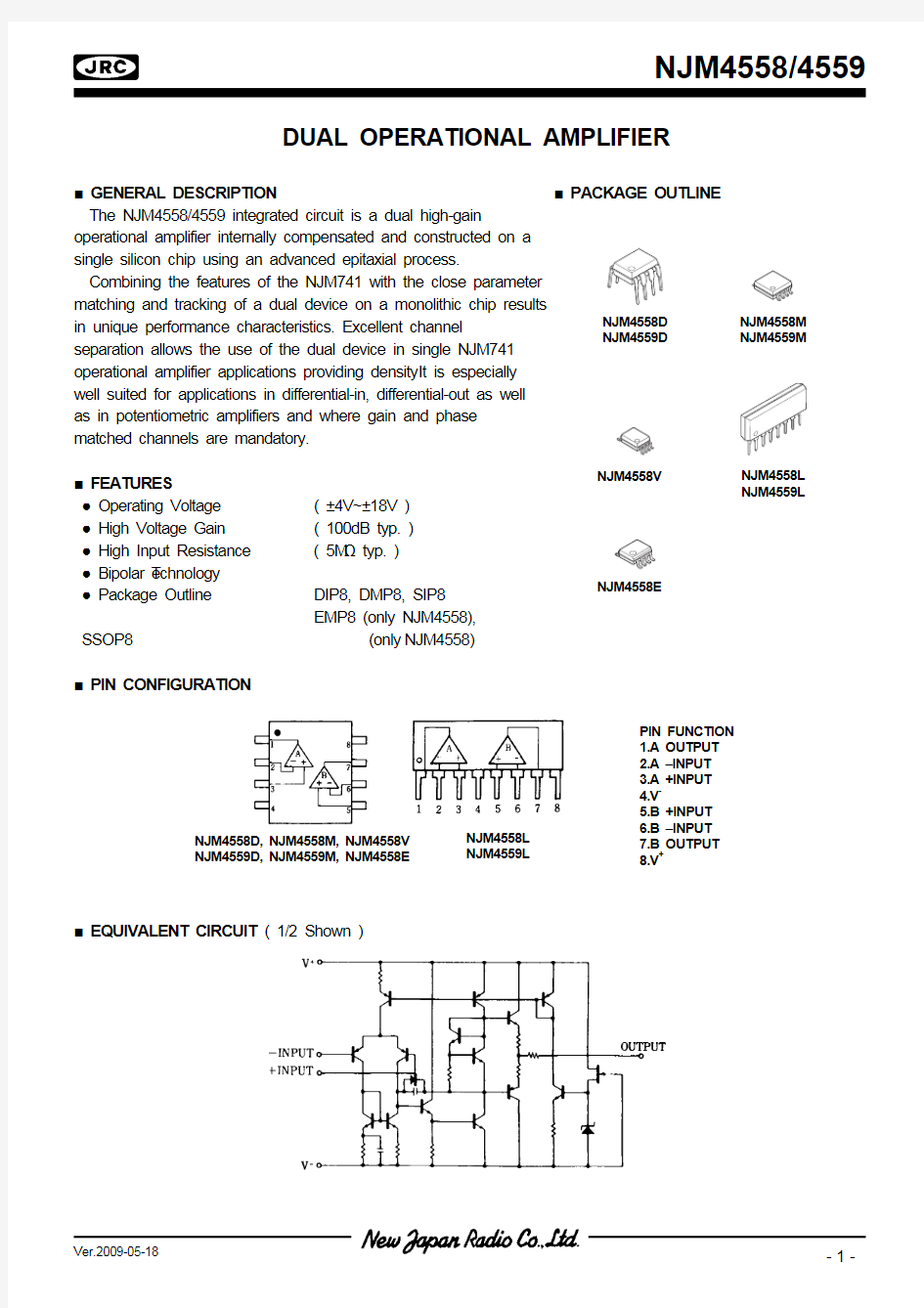
■ GENERAL DESCRIPTION ■ PACKAGE OUTLINE The NJM4558/4559 integrated circuit is a dual high-gain operational amplifier internally compensated and constructed on a single silicon chip using an advanced epitaxial process.
Combining the features of the NJM741 with the close parameter matching and tracking of a dual device on a monolithic chip results
in unique performance characteristics. Excellent channel
separation allows the use of the dual device in single NJM741 operational amplifier applications providing density . It is especially well suited for applications in differential-in, differential-out as well as in potentiometric amplifiers and where gain and phase matched channels are mandatory.
■ FEATURES
● Operating Voltage ( ±4V~±18V ) ● High Voltage Gain ( 100dB typ. ) ● High Input Resistance ( 5M ? typ. ) ● Bipolar T echnology
● Package Outline DIP8, DMP8, SIP8 EMP8 (only NJM4558),
SSOP8 (only NJM4558)
■ PIN CONFIGURATION
■ EQUIVALENT CIRCUIT ( 1/2 Shown )
NJM4558L NJM4559L
NJM4558M NJM4559M
NJM4558V
NJM4558D, NJM4558M, NJM4558V NJM4559D, NJM4559M, NJM4558E NJM4558L NJM4559L PIN FUNCTION
1.A OUTPUT
2.A –INPUT
3.A +INPUT
4.V -
5.B +INPUT
6.B –INPUT
7.B OUTPUT 8.V +
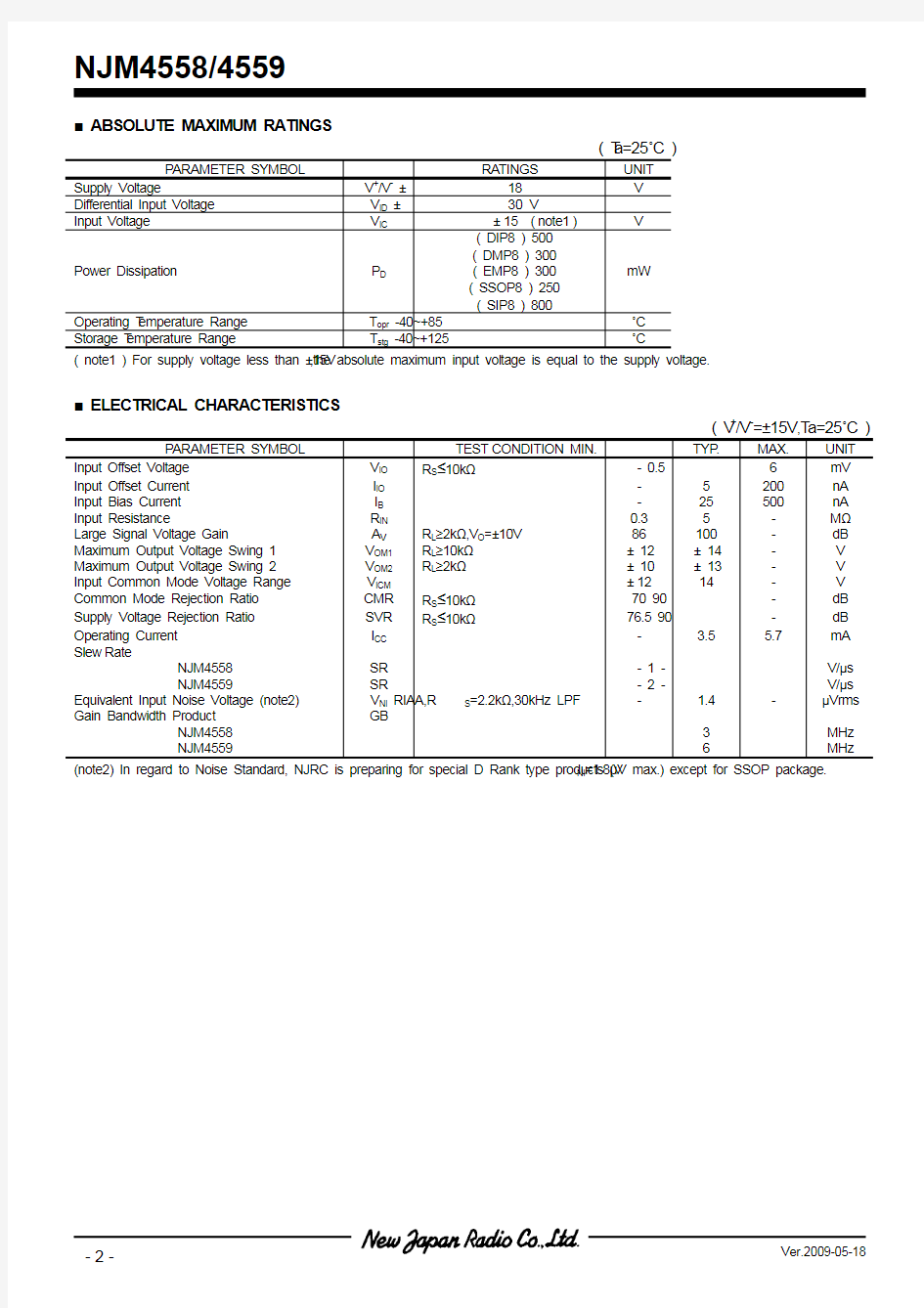
■ ABSOLUTE MAXIMUM RATINGS
( T a=25?C )
UNIT
P ARAMETER SYMBOL RA TINGS
Supply Voltage V+/V- ±
18 V
30 V
Differential Input Voltage V ID ±
Input Voltage V IC ± 15 ( note1 ) V
( DIP8 ) 500
( DMP8 ) 300
Power Dissipation P D
mW
( EMP8 ) 300
( SSOP8 ) 250
( SIP8 ) 800
Operating T emperature Range T opr -40~+85 ?C
Storage T emperature Range T stg -40~+125 ?C
( note1 ) For supply voltage less than ±15V,the absolute maximum input voltage is equal to the supply voltage.
■ ELECTRICAL CHARACTERISTICS
( V+/V-=±15V,T a=25?C )
UNIT
MAX.
TYP.
CONDITION MIN.
P ARAMETER SYMBOL TEST
Input Offset Voltage V IO R
≤10k?- 0.5 6 mV
S
Input Offset Current I IO- 5 200 nA
Input Bias Current I B- 25 500 nA
Input Resistance R IN0.3 5 - M?
Large Signal Voltage Gain A V R L≥2k?,V O=±10V 86 100 - dB
Maximum Output Voltage Swing 1 V OM1R L≥10k?± 12 ± 14 - V
Maximum Output Voltage Swing 2 V OM2R L≥2k?± 10 ± 13 - V
12 14 - V
Input Common Mode Voltage Range V ICM±
Common Mode Rejection Ratio CMR R
≤10k?70 90 - dB
S
Supply Voltage Rejection Ratio SVR R
≤10k?76.5 90 - dB
S
Operating Current I CC- 3.5 5.7 mA
Slew
Rate
NJM4558 SR - 1 - V/μs
NJM4559 SR - 2 - V/μs
Equivalent Input Noise Voltage (note2) V NI RIAA,R S=2.2k?,30kHz LPF - 1.4 - μVrms
Gain Bandwidth Product GB
MHz NJM4558 3
MHz NJM4559 6
(note2) In regard to Noise Standard, NJRC is preparing for special D Rank type products (V NI=1.8μV max.) except for SSOP package.