安捷伦 A5000系列(S5008) 光学鼠标芯片资料Datasheet

ADNS-5000 Optical Mouse Sensor Data Sheet
Description
The ADNS-5000 is a one-chip USB optical mouse sensor for implementing a non-mechanical tracking engine for computer mice.
It is based on optical navigation technology that measures changes in position by optically acquiring sequential surface images (frames) and mathemati-cally determining the direction and magnitude of move-ment.
The sensor is in a 18-pin optical package that is designed to be used with the ADNS-5100 Round Lens or ADNS-5100-001 Trim Lens, the ADNS-5200 Clip, and the HLMP-ED80-XX000 LED. These parts provide a complete and compact mouse sensor. There are no moving parts, and precision optical alignment is not required, facilitating high volume assembly.
The output format is USB. This device meets USB revision
1.1 speci?cations and is compatible with USB Revision
2.0 speci?cation.
Default resolution is speci?ed as 500 counts per inch, with rates of motion up to 16 inches per second and 2g acceleration. Resolution can also be programmed to 1000 cpi. Frame rate is varied internally by the sensor to achieve tracking and speed performance, eliminating the need for the use of many registers.
A complete mouse can be built with the addition of a PC board, switches, mechanical Z-wheel, plastic case and cable. A 1% pull up resistor is needed for the US
B port to signify a low speed HID device.Features
x Optical navigation technology
x No mechanical moving parts
x High reliability
x Complete 2-D motion sensor
x High speed motion detection
x Accurate navigation over a wide variety of surfaces x No precision optical alignment needed
x Wave Solderable
x IEC 60825-1 eye safe under single fault conditions
x Single 5.0 volt power supply
x Meets USB Revision 1.1 Speci?cation and compatible with USB Revision 2.0 speci?cation
x Meets HID Revision 1.1
x On Chip LED Drive with regulated current Applications
x Mice for desktop PC’s, Workstations, and portable PC’s
x Trackballs
x
Integrated input devices
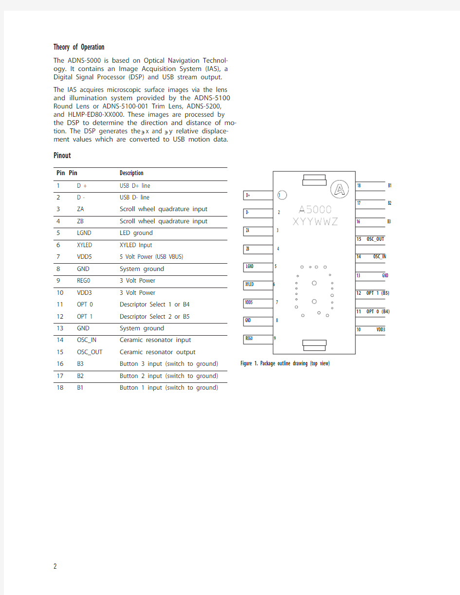
Figure 1. Package outline drawing (top view)
Theory of Operation
The ADNS-5000 is based on Optical Navigation Technol-ogy. It contains an Image Acquisition System (IAS), a Digital Signal Processor (DSP) and USB stream output.The IAS acquires microscopic surface images via the lens and illumination system provided by the ADNS-5100 Round Lens or ADNS-5100-001 Trim Lens, ADNS-5200, and HLMP-ED80-XX000. These images are processed by the DSP to determine the direction and distance of mo-tion. The DSP generates the 'x and 'y relative displace-ment values which are converted to USB motion data.
Pinout
Pin Pin
Description
1 D +USB D+ line
2 D -USB D- line
3ZA Scroll wheel quadrature input 4ZB Scroll wheel quadrature input 5LGND LED ground 6XYLED XYLED Input
7VDD5 5 Volt Power (USB VBUS)8GND System ground 9REG0 3 Volt Power 10VDD3 3 Volt Power
11OPT 0Descriptor Select 1 or B412OPT 1Descriptor Select 2 or B513GND System ground 14OSC_IN Ceramic resonator input 15OSC_OUT Ceramic resonator output 16B3Button 3 input (switch to ground)17B2Button 2 input (switch to ground)18
B1
Button 1 input (switch to ground)
11 OPT 0 (B4)
12 OPT 1 (B5)
15 OSC_OUT
14 OSC_IN
13 GND
18 B1
17 B2
16 B310 VDD3
GND 8
VDD5 7
ZB 4
LGND 5
XYLED 6
D+ 1
D- 2
ZA 3
REG0 9
Figure 2. Package outline drawing
CAUTION: It is advised that normal static precautions be taken in handling and assembly
of this component to prevent damage and/or degradation which may be induced by ESD.
scribing the base plate molding features for lens and PCB alignment.
Figure 4. 2D assembly drawing of ADNS-5000
Figure 3. Recommended PCB mechanical cutouts and spacing (Top view)
The components interlock as they are mounted onto de?ned features on the base plate.
The ADNS-5000 sensor is designed for mounting on a through hole PCB, looking down. The aperture stop and features on the package align it to the lens (See ?gure 3).
The ADNS-5100 Round lens provides optics for the imag-ing of the surface as well as illumination of the surface at the optimum angle. Lens features align it to the sensor, base plate, and clip with the LED. The lens also has a large
Figure 5. Exploded view drawing
round ?ange to provide a long creepage path for any ESD events that occur at the opening of the base plate (See ?gure 4).
The ADNS-5200 clip holds the LED in relation to the lens. The LED must be inserted into the clip and the LED’s leads formed prior to loading on the PCB.
The HLMP-ED80-XX000 LED is recommended for illumi-nation. If used with the bin table, su?cient illumination can be guaranteed.
Block Diagram
Figure 6. Block Diagram
ZB
ZA
Z WHEEL
OSCILLATOR
LED OSC_OUT
VOLTAGE REFERENCE D -USB PORT
5 VOLT POWER
BUTTONS
B4B3B2B1B5
PCB Assembly Considerations
1. Insert the sensor and all other electrical components into PCB.
2. Bend the LED leads 90 degrees and then insert the Led into the assembly clip until the snap feature locks the Led base.
3. Insert the LED/clip assembly into PCB.
4. Wave solder the entire assembly in a no-wash solder process utilizing solder ?xture. The solder ?xture is needed to protect the sensor during the solder process. The ?xture should be designed to expose the sensor leads to solder while shielding the optical aperture from direct solder contact.
5. Place the lens onto the base plate.
6. Remove the protective Kapton tape from optical aperture of the sensor. Care must be taken to keep contaminants from entering the aperture. Recom-mend not placing the PCB facing up during the entire mouse assembly process. Recommend to hold the PCB ?rst vertically for the Kapton removal process.
7. Insert PCB assembly over the lens onto base plate aligning post to retain PCB assembly. The sensor ap-erture ring should self-align to the lens.
8. The optical position reference for the PCB is set by the base plate and lens. Note that the PCB motion due to button presses must be minimized to maintain optical alignment.
9. Install mouse top case.
Figure 7. Typical Application
Design considerations for improving ESD Performance
The table below shows typical values assuming base plate construction per the Avago Technologies supplied IGES ?le and ADNS-5100 Round lens.Typical distance
A5100
A5100-001
Creepage 40.5mm 17.9mm Clearance
32.6mm
9.2mm
Typical Application
Regulatory Requirements
x Passes F CC B and worldwide analogous emission limits when assembled into a mouse with unshielded cable and following Avago Technologies recommen-dations.
x Passes EN61000-4-4/IEC801-4 EFT tests when assem-bled into a mouse with shielded cable and following Avago Technologies recommendations.x UL ?ammability level UL94 V-0.
x Provides su?cient ESD creepage/clearance distance to avoid discharge up to 15kV when assembled into a mouse according to usage instructions above.
Notes on bypass capacitors:
x All caps (except C4) MUST be as close to the sensor pins as possible.
x Caps should be ceramic.
x Caps should have less than 5 nH of self inductance x Caps connected to VDD3 MUST have less than 0.2: ESR
x 1.5k : resistor should be ± 1% tolerance.
x Z-wheel connections are detailed in Figure 20
x Buttons B1-B5 can be used as button or VID/PID straps (see strap table on page 14). For VID/PID connections, parts must be connected to Vdd3 on ‘high’ connec-tion, preferably near pin 10
Surface mount parts are recommended
Figure 8. Application Schematic for 3 buttons and 5 buttons
Absolute Maximum Ratings
Recommended Operating Conditions
Figure 9. Distance from lens reference plane to object surface
Parameter
Symbol
Minimum
Maximum
Units
Notes
Storage Temperature T S -4085 q C Operating Temperature T A
-15
55 q C Lead Solder Temp 260 q C For 10 seconds, 1.6mm below seating plane.
Supply Voltage V DD
-0.5
5.5 V ESD 2 kV All pins, human body model MIL 883 Method 3015
Input Voltage V IN -0.5V DD +0.5 V All I/O pins except OSC_IN and OSC_OUT, D+, D- Input Voltage V IN -1.0 4.6 V D+, D-, AC waveform, see USB speci?cation (7.1.1)
Input Voltage
V IN -0.5 3.6 V OSC_IN and OSC_OUT
Input Short Circuit Voltage
V SC
V DD
V
D+, D-, see USB speci?cation (7.1.1)
Parameter
Symbol
Minimum
Typical
Maximum
Units
Notes
Operating Temperature T A 040 q C Power supply voltage V DD 4.0 5.0 5.25Volts For accurate navigation and proper USB operation
Power supply voltage V dd 3.8 5.0
5.25Volts Maintains communication to USB host and internal register contents.Power supply rise time V RT 0.1
100ms Supply noise V N 100mV Peak to peak within 0-100 MHz bandwidth
Velocity Vel 16
ips Acceleration Acc 2 G
Clock Frequency f clk 23.642424.36MHz Due to USB timing constraints Resonator Impedance X RES 55 :Distance from lens refer-ence plane to surface Z 2.3 2.4
2.5mm See Figure 9 Light Level onto IC
IRR INC
80100
25,00030,000
mW/m 2
=639nm =875nm
Electrical Characteristics over recommended operating conditions. Typical values at 25 °C, V DD =5.0 V, 24MHz USB Electrical Speci?cations
Electrical Characteristics over recommended operating conditions. Parameter
Symbol
Min.
Typ.
Max.
Units
Notes
Power up delay T PUP 50ms Debounce delay on button inputs T DBB
5
9
17
ms
“Maximum” speci?ed at 8ms polling rate. Mechanical Z-Wheel Internally pulled down with 20k resistors and debounced
Transient Supply Current
I DDT
60
mA
Max. supply current during a VDD ramp from 0 to 5.0 V with > 500 s rise time. Does not include charging currents for bypass capacitors.Input Capacitance
(OSC Pins)
C OSC_IN
50pF
OCS_IN, OSC_OUT to GND
Parameter
Symbol
Min.
Max.
Units
Notes
Output Signal Crossover Voltage V CRS 1.3 2.0V C L = 200 to 600 pF (see Figure 10)Input Signal Crossover Voltage V ICRS 1.2 2.1V C L = 200 to 600 pF (see Figure 10)
Output High V OH 2.8 3.6V with 15 kohm to Ground and 7.5 k to Vbus on D- (see Figure 11)
Output Low V OL 0.0
0.3V with 15 kohm to Ground and 7.5 k to Vbus on D- (see Figure 11)
Single Ended Output V SE00.8
V Input High (Driven)VI H 2.0V Input High (Floating)V IHZ 2.7 3.6V Input Low
V IL 0.8
V 7.5k to Vdd5
Di?erential Input Sensitivity V DI 0.2V |(D+)-(D-)| See Figure 12Di?erential Input Common Mode Range
V CM 0.8 2.5V Includes V DI , See Figure 12
Single Ended Receiver Threshold V SE 0.8
2.0V Transceiver Input Capacitance
C IN
12pF
D+ to V BUS , D- to V BUS
Timing Speci?cations over recommended operating conditions.
Parameter Symbol Min.Max.Units Notes
D+/D- Transition rise time T LR75ns C L = 200 pF (10% to 90%), see Figure 10
D+/D- Transition rise time T LR300ns C L = 600 pF (10% to 90%), see Figure 10
D+/D- Transition fall time T LF75ns C L = 200 pF (90% to 10%), see Figure 10
D+/D- Transition fall time T LF300ns C L = 600 pF (90% to 10%), see Figure 10
Rise and Fall time matching T LRFM80125%T R/T F; C L = 200 pF; Excluding the ?rst transition
from the Idle State
Wakeup delay from USB suspend mode due to buttons push T WUPB17ms Delay from button push to USB operation
Only required if remote wakeup enabled
Wakeup delay from USB suspend mode due to buttons push until accurate navigation T WUPN50ms Delay from button push to navigation operation
Only required if remote wakeup enabled
USB reset time T reset18.7s
Data Rate t LDRATE 1.4775 1.5225Mb/s Average bit rate, 1.5 Mb/s +/- 1.5% Receiver Jitter Tolerance t DJR1-7575ns To next transition, see Figure 13 Receiver Jitter Tolerance t DJR2-4545ns For paired transitions, see Figure 13 Di?erential to EOP Transition
Skew
t LDEOP-40100ns See Figure 14
EOP Width at Receiver t LEOPR670ns Accepts EOP, see Figure 14
Source EOP Width t LEOPT 1.25 1.50s
Width of SE0 interval during
Di?erential Transition
t LST210ns See Figure 11.
Di?erential Output Jitter t UDJ1-9595ns To next transition, see Figure 15
Di?erential Output Jitter t UDJ2-150150ns For paired transitions, see Figure 15
Figure 10. Data Signal Rise and Fall Times
Figure 11. Data Signal Voltage Levels
Figure 12. Di?erential Receiver Input Sensitivity vs. Common Mode Input Range
V CRS
Rise Time
Fall Time
V OL
V OH V OH (min)V OL (max)
GND
V IH (min)V IL (max)t LST
Input Voltage Range (volts)
Figure 13. Receiver Jitter Tolerance
Figure 14. Di?erential to EOP Transition Skew and EOP Width
Figure 15. Di?erential Output Jitter
T PERIOD
PERIOD DJR2
Data T PERIOD
Differential Data Lines
T PERIOD
Differential Data Lines
DC Electrical Speci?cations
Electrical Characteristics over recommended operating conditions. Typical values at 25 °C, V DD =5.0 V, 24MHz Parameter
Symbol
Minimum Typical
Maximum Units
Notes
Supply current (Sensor only), mouse moving I DDS 7.2mA No load on B1-B3, Z-LED, XYLED ZA, ZB, D+, D-Supply current (Sensor only), mouse not moving I DDSN 6.2
mA
No load on B1-B3, Z-LED, XYLED ZA, ZB, D+, D-Supply current, USB suspend mode I DDSS 250 P A No load on B1-B3, Z-LED, XYLED ZA, ZB, D+, D-XYLED current I LED 30mA XYLED Output Low Voltage V OL 1.1V Refer to Figure 16
Input Low Voltage
V IL
0.5
V
Pins: ZA, ZB, B1, B2, B3, V IL max of 0.5V DC is at V DD min of 4V DC , with a typical of 0.8V DC at V DD of 5V DC Input High Voltage V IH 0.6*V DD
V Pins: ZA, ZB, B1, B2, B3 Input Hysteresis V HYST 285mV Pins: ZA, B1, B2, Input Hysteresis V HYST 200
mV Pins: ZB Button Pull Up Current
B IOUT
125
275
500
A
Pins: B1, B2, B3
Typical Performance Characteristics
Performance Characteristics over recommended operating conditions. Typical values at 25 °C, V DD =5.0 V, 24MHz Parameter Symbol Minimum Typical
Maximum Units
Notes
Path Error (Deviation)
P Error
0.5
%
Average path error as percent of total
2.5” travel on various standard surfaces
Typical Performance Characteristics
Performance Characteristics over recommended op-erating conditions. Typical values at 25 °C, V DD =5.0 V, 24MHz
Figure 16. Typical Resolution vs. Z [2,3]
Figure 17. Wavelength responsivity.[1] (Comparative Surfaces)
The following graphs are the typical performance of the ADNS-5000 sensor, assembled as shown in the 2D assem-bly drawing with the ADNS-5100 Round Lens/Prism, the ADNS-5200 clip, and the HLMP-ED80-XX000 LED.
00.10.20.30.40.50.60.70.80.91400
500
600700800900
1000
Wavelength in nm
N o r m a l i s e d r e s p o n s e
Notes:
1. The ADNS-5000 is designed for optimal performance when used with the HLMP-ED80-XX000 (Red LED 639nm).
2. Z = distance from Lens Reference Plane to Surface.
3. DOF = Depth of Field
11-0.8
-0.6
-0.4
-0.2
0.2
0.4
0.6
0.8
1
Z-H eight(mm)
R e s o l u t i o n (D P I )
Con?guration after Power up (Data Values)
Signal Function State from Figure 9-1 of USB spec:
Powered or Default Address or Con?gured
State from Figure 9-1 of USB spec:
Suspended from any other state
B1Hi-Z if tied to VDD3 else pullup active Hi-Z if tied to VDD3 else pullup active
B2Hi-Z if tied to VDD3 else pullup active Hi-Z if tied to VDD3 else pullup active
B3Hi-Z if tied to VDD3 else pullup active Hi-Z if tied to VDD3 else pullup active
B4Hi-Z if tied to VDD3 else pullup active Hi-Z if tied to VDD3 else pullup active
B5Hi-Z if tied to VDD3 else pullup active Hi-Z if tied to VDD3 else pullup active
D-USB I/O Hi-Z input
D+USB I/O Hi-Z input
OSC_IN24MHz pulled low
OSC_OUT24MHz
XYLED low (on) or pulsing Pulled high (o?)
ZB/Z_LED Hi-Z input Hi-Z input
ZA Hi-Z if ZA tied to GND Hi-Z input
Strap (Jumper) Table
The PID/string strap matrix is the following:
Mouse type VID PID Manuf str. Product string B1B2 B3 OPT 0OPT 1ZA ZB
3-button mse 0x192F0x0116“““USB Optical
Mouse”
sw1 sw2 sw3Vdd3 Vdd3mech
Z-wheel
mech
Z-wheel
5-button mse 0x192F 0x0216“““USB Optical
Mouse”
sw1 sw2 sw3sw4 sw5mech
Z-wheel
mech
Z-wheel
XY LED
x The peak current values are 30 mA if R1 59ohm and the part meets the IEC 825-1 eye safety regulations.
Buttons
The minimum time between button presses is T DBB . But-tons B1 through B3 are connected to a Schmidt trigger input with 100 uA current sources pulling up to +5 volts during normal, sleep and USB suspend modes.
Notes:
For mechanical Z-wheels the following must be imple-mented:
x Use a rotary switch equivalent to the Panasonic part EVQVX at https://www.360docs.net/doc/4117718897.html,/www-data/pdf/ATC0000/ATC0000CE20.pdf (The key point is stable “A” switch state in all detent positions).
x Solder the rotary switch into the PCB such that the common pin is closest to the cable end of the mouse. (Metal plate faces to left)
x Connect the “A” terminal of the rotary switch to “ZA” and the “B” terminal to “ZB”. ZA MUST be connected to “Signal A” in Figure 19 where the z-wheel detents are mechanically stable.
Figure 19. Z-Wheel A and B connections
Z-Wheel
The mechanical Z-Wheel connections (A,B) are deter-mined below.
X & Y Directions
(Looking through an ADNS-5100 Lens)
The positive and negative X and Y directions with respect to the mouse case are shown in the diagram below.
Top Xray View of Mouse
POSITIVE X
P O S T E Y
I I V Figure 18. Directions are for a complete mouse, with the ADNS-5100 lens
USB Commands
Mnemonic Command Notes
USB_RESET D+/D- low > 18.6 us Device Resets; Address=0
USB_SUSPEND Idle state > 3mS Device enters USB low-power mode
USB_RESUME Non-idle state Device exits USB low-power mode
Get_Status_Device80 00 00 00 00 00 02 00Normally returns 00 00, Self powered 00 00,
Remote wakeup 02 00
Get_Status_Interface81 00 00 00 00 00 02 00Normally returns 00 00
Get_Status_Endpt082 00 00 00 xx 00 02 00OUT: xx=00, IN: xx=80Normally returns 00 00
Get_Status_Endpt182 00 00 00 81 00 02 00Normally returns 00 00, Halt 00 01
Get_Con?guration80 08 00 00 00 00 01 00Return: 00=not con?g., 01=con?gured
Get_Interface81 0A 00 00 00 00 01 00Normally returns 00
Get_Protocol A1 03 00 00 00 00 01 00Normally returns 01, Boot protocol 00
Get_Desc_Device80 06 00 01 00 00 nn 00See USB command details
Get_Desc_Con?g80 06 00 02 00 00 nn 00See USB command details
Get_Desc_String80 06 xx 03 00 00 nn 00See USB command details
Get_Desc_HID81 06 00 21 00 00 09 00See USB command details
Get_Desc_HID_Report81 06 00 22 00 00 nn 00See USB command details
Get_HID_Input A1 01 00 01 00 00 nn 00Return depends on motion & con?g
Get_Idle A1 02 00 00 00 00 01 00Returns rate in multiples of 4ms
Get_Vendor_Test C0 01 00 00 xx 00 01 00Read register xx
Set_Address00 05 xx 00 00 00 00 00xx = address
Set_Con?guration00 09 xx 00 00 00 00 00Not con?gured: xx=00Con?gured: xx=01
Set_Interface01 0B 00 00 00 00 00 00Only one interface supported
Set_Protocol21 0B xx 00 00 00 00 00Boot: xx=00, Report: xx=01
Set_Feature_Device00 03 01 00 00 00 00 00Enable remote wakeup
Set_Feature_Endpt002 03 00 00 xx 00 00 00Halt. OUT: xx=00, IN: xx=80
Set_Feature_Endpt102 03 00 00 81 00 00 00Halt
Clear_Feature_Device00 01 01 00 00 00 00 00Disable Remote wakeup
Clear_Feature_Endpt002 01 00 00 xx 00 00 00Clear Halt; OUT: xx=00, IN: xx=80
Clear_Feature_Endpt102 01 00 00 81 00 00 00Clear Halt
Set_Idle21 0A 00 rr 00 00 00 00rr = report rate in multiples of 4ms
Set_Vendor_Test40 01 00 00 xx yy 00 00Write yy to address xx
Poll_Endpt1Read buttons, motion, & Z-wheel
Note:
The last two bytes in a command shown as “nn 00” specify the 16-bit data size in the order of “LowByte HighByte.” For example a two-byte data size would be specifed as “02 00.” ADNS-5000 will not provide more bytes than the number requested in the command, but it will only supply up to a maximum of 8 bytes at a time. The ADNS-5000 will re-send the last packet if the transfer is not acknowledged properly.
USB COMMAND DETAILS
___________________________________________________________________________________________
USB_RESET D+/D- low for an extended period
USB Spec: A device may reset after seeing an SE0 for more than 18.6 uS, and de?nitely after 10mS. Notes: After power up and prior to Reset, the device will not respond to any USB commands. After the device has been given a USB Reset, the device’s address will be reset to zero and the device will be in the Default state. The chip will default to Report protocol and any pending output will be ?ushed.
___________________________________________________________________________________________USB_SUSPEND Idle state for an extended period USB Spec: A device may suspend after seeing an idle for more than 3mS, and de?nitely after 10mS. Notes: The chip will take a minimum of 5mS to start Suspend, though will de?nitely start after 6mS. The chip may ?nish the current frame if necessary before stopping the clock. Thus, an additional frame time may be used to reach Suspend mode.___________________________________________________________________________________________USB_RESUME Non-idle state USB Spec: Remote Resume signalling from a device must be between 1mS and 15mS. The host is required to send Resume signaling for 20mS plus 10mS of resume recovery time in which it does not access any devices. This allows devices enough time to wake back up. Notes: The chip can cause a Resume if Remote Wakeup is enabled and a button has been pressed.
Remote resume signalling from the chip will last 11.45mS to 12.45mS.
___________________________________________________________________________________________Get_Status_Device 80 00 00 00 00 00 02 00 Returns: xx yy xx[0] = Self Powered xx[1] = Remote Wakeup xx[7:2] = 0 yy = 00 (Reserved) Default: Accept (unde?ned in USB Spec) Addressed: Accept Con?gured: Accept Notes: Use Set_Feature_Device/Clear_Feature_Device to set/clear remote wakeup.___________________________________________________________________________________________Get_Status_Interface 81 00 00 00 00 00 02 00 Returns: 00 00 Default: Stall (unde?ned in USB Spec) Addressed: Stall Con?gured: Accept Notes: Both return bytes are reserved and currently 00.___________________________________________________________________________________________Get_Status_Endpt0 82 00 00 00 xx 00 02 00 82 00 00 00 00 00 02 00 82 00 00 00 80 00 02 00 xx = 00 = Endpt0 OUT xx = 80 = Endpt0 IN Returns: xx yy xx[0] = H alt xx[7:1] = 0 yy = 00 (Reserved) Default: Accept (unde?ned in USB Spec) Addressed: Accept Con?gured: Accept Notes: Use Set_Feature_Endpt0/Clear_Feature_Endpt0 to (try to) set/clear Halt bit. According to USB, “It is neither required or recommended that the Halt feature be implemented for the Default Control Pipe.” Since a new SETUP command will clear any Endpt0 halt bit, it is
____________________________________________________________________________________________Get_Status_Endpt1 82 00 00 00 81 00 02 00 Returns: xx yy xx[0] = H
alt xx[7:1] = 0 yy = 00 (Reserved) Default: Stall (unde?ned in USB Spec) Addressed: Stall Con?gured: Accept Notes: Use Set_Feature_Endpt1/Clear_Feature_Endpt1 to set/clear Halt bit.___________________________________________________________________________________________Get_Con?guration 80 08 00 00 00 00 01 00 Returns: xx xx = con?g value
Default: Accept (unde?ned in USB Spec) — returns 00
Addressed: Accept — returns 00 Con?gured: Accept — returns 01 Notes: Use Set_Con?guration to change.___________________________________________________________________________________________Get_Interface 81 0A 00 00 00 00 01 00 Returns: 00 Default: Unde?ned in USB Spec Addressed: Stall Con?gured: Accept — returns 00 Notes: Command has no alternate interfaces, so only valid value is 00___________________________________________________________________________________________Get_Protocol A1 03 00 00 00 00 01 00 Returns: xx xx = 00 = Boot protocol xx = 01 = Report protocol
Default: Accept
Addressed: Accept Con?gured: Accept Notes: Defaults to Report protocol after USB Reset. Use Set_Protocol to change.___________________________________________________________________________________________Get_Desc_Device 80 06 00 01 00 00 nn00
80 06 00 01 00 00 12 00 Returns: 12 01 00 02 00 00 00 08 vv vv pp pp dd dd mm PP ss 01 vv vv = vendor id pp pp = product id (vendor speci?ed) dd dd = device id (vendor speci?ed) (bcd rev_id byte) mm = iManufacturer PP = iProduct ss = iSerialNumber (00 - no string)
Default: Accept Addressed: Accept Con?gured: Accept
___________________________________________________________________________________________
Get_Desc_Con?g
80 06 00 02 00 00 nn 00 80 06 00 02 00 00 22 00
Returns: 09 02 22 00 01 01 00 A0 32 09 04 00 00 01 03 01 02 00 09 21 10 01 00 01 22 rr 00 07 05 81 03 04 00 0A rr = HID Report descriptor length
These values are determined by jumper con?guration see strap table.
Without Z-Wheel: 09 02 22 00 01 01 00 A0 32 09 04 00 00 01 03 01 02 00 09 21 10 01 00 01
22 32 00 07 05 81 03 04
00 0A
// Con?g Descriptor | 09 // bLength | 02 // bDescriptorType | 22 // wTotalLength (34 decimal) | 00 // high byte of WTotalLength | 01 // bNumInterfaces | 01 // bCon?gurationValue | 00 // iCon?guration | A0 // bmAttributes (bus powered/remote wakeup) | 32 // MaxPower (in 100mA in 2mA units) // Interface Descriptor | 09 // bLength | 04 // bDescriptorType | 00 // bInterfaceNumber | 00 // bAlternateSetting | 01 // bNumEndpoints | 03 // bInterfaceClass (HID Class) | 01 // bInterfaceSubClass | 02 // bInterfaceProtocol | 00 // iInterface // H ID Descriptor | 09 // bLength | 21 // bDescriptorType | 11 // bcdHID ( HID Release ##.##; HID 1.1 compliant ) | 01 // | 00 // bCountry | 01 // bAvailable | 22 // bType | 32 // wLength (Length of HID Report below) | 00 // // Endpoint Descriptor | 07 // bLength | 05 // bDescriptorType | 81 // bEndpointAddress (IN & #=1) | 03 // bmAttributes (Interrupt) | 04 // wMaxPacketSize | 00 // | 0A // bInterval (10mS)
With Z-Wheel:
09 02 22 00 01 01 00 A0 32 09 04 00 00 01 03 01 02 00 09 21 10 01 00 01 22 34 00 07 05 81 03 04 00 0A
// Con?g Descriptor | 09 // bLength | 02 // bDescriptorType | 22 // wTotalLength (34 decimal)
| 00 // high byte of WTotalLength | 01 // bNumInterfaces | 01 // bCon?gurationValue | 00 // iCon?guration | A0 // bmAttributes (bus powered/remote wakeup) | 32 // MaxPower (in 100mA in 2mA units) // Interface Descriptor | 09 // bLength | 04 // bDescriptorType | 00 // bInterfaceNumber | 00 // bAlternateSetting | 01 // bNumEndpoints | 03 // bInterfaceClass (HID Class) | 01 // bInterfaceSubClass | 02 // bInterfaceProtocol | 00 // iInterface // H ID Descriptor | 09 // bLength | 21 // bDescriptorType | 11 // bcdHID ( HID Release ##.##; HID 1.1 compliant ) | 01 // | 00 // bCountry | 01 // bAvailable | 22 // bType | 34 // wLength (Length of HID Report below) | 00 // // Endpoint Descriptor | 07 // bLength | 05 // bDescriptorType | 81 // bEndpointAddress (IN & #=1) | 03 // bmAttributes (Interrupt) | 04 // wMaxPacketSize | 00 // | 0A // bInterval (10mS) Default: Accept Addressed: Accept Con?gured: Accept Notes: This is the concatenation of 4 descriptors: Con?guration Interface H
ID
Endpt
74系列芯片--HD74LS174
Hitachi Code JEDEC EIAJ Weight (reference value)DP-16 Conforms Conforms 1.07 g Unit: mm
Hitachi Code JEDEC EIAJ Weight (reference value)FP-16DA —Conforms 0.24 g *Dimension including the plating thickness Base material dimension ° – 8°
Hitachi Code JEDEC EIAJ Weight (reference value)FP-16DN Conforms Conforms 0.15 g *Dimension including the plating thickness Base material dimension ° – 8°
Cautions 1.Hitachi neither warrants nor grants licenses of any rights of Hitachi’s or any third party’s patent, copyright, trademark, or other intellectual property rights for information contained in this document.Hitachi bears no responsibility for problems that may arise with third party’s rights, including intellectual property rights, in connection with use of the information contained in this document. 2.Products and product specifications may be subject to change without notice. Confirm that you have received the latest product standards or specifications before final design, purchase or use. 3.Hitachi makes every attempt to ensure that its products are of high quality and reliability. However, contact Hitachi’s sales office before using the product in an application that demands especially high quality and reliability or where its failure or malfunction may directly threaten human life or cause risk of bodily injury, such as aerospace, aeronautics, nuclear power, combustion control, transportation,traffic, safety equipment or medical equipment for life support. 4.Design your application so that the product is used within the ranges guaranteed by Hitachi particularly for maximum rating, operating supply voltage range, heat radiation characteristics, installation conditions and other characteristics. Hitachi bears no responsibility for failure or damage when used beyond the guaranteed ranges. Even within the guaranteed ranges, consider normally foreseeable failure rates or failure modes in semiconductor devices and employ systemic measures such as fail-safes, so that the equipment incorporating Hitachi product does not cause bodily injury, fire or other consequential damage due to operation of the Hitachi product. 5.This product is not designed to be radiation resistant. 6.No one is permitted to reproduce or duplicate, in any form, the whole or part of this document without written approval from Hitachi. 7.Contact Hitachi’s sales office for any questions regarding this document or Hitachi semiconductor products. Hitachi, Ltd. Semiconductor & Integrated Circuits.Nippon Bldg., 2-6-2, Ohte-machi, Chiyoda-ku, Tokyo 100-0004, Japan Tel: Tokyo (03) 3270-2111 Fax: (03) 3270-5109Copyright ' Hitachi, Ltd., 1999. All rights reserved. Printed in Japan.Hitachi Asia Pte. Ltd.16 Collyer Quay #20-00Hitachi Tower Singapore 049318Tel: 535-2100Fax: 535-1533URL NorthAmerica : http:https://www.360docs.net/doc/4117718897.html,/Europe : https://www.360docs.net/doc/4117718897.html,/hel/ecg Asia (Singapore): https://www.360docs.net/doc/4117718897.html,.sg/grp3/sicd/index.htm Asia (Taiwan): https://www.360docs.net/doc/4117718897.html,/E/Product/SICD_Frame.htm Asia (HongKong): https://www.360docs.net/doc/4117718897.html,/eng/bo/grp3/index.htm Japan : http://www.hitachi.co.jp/Sicd/indx.htm Hitachi Asia Ltd.Taipei Branch Office 3F, Hung Kuo Building. No.167, Tun-Hwa North Road, Taipei (105)Tel: <886> (2) 2718-3666Fax: <886> (2) 2718-8180Hitachi Asia (Hong Kong) Ltd.Group III (Electronic Components)7/F., North Tower, World Finance Centre,Harbour City, Canton Road, Tsim Sha Tsui,Kowloon, Hong Kong Tel: <852> (2) 735 9218Fax: <852> (2) 730 0281 Telex: 40815 HITEC HX Hitachi Europe Ltd. Electronic Components Group. Whitebrook Park Lower Cookham Road Maidenhead Berkshire SL6 8YA, United Kingdom Tel: <44> (1628) 585000 Fax: <44> (1628) 778322Hitachi Europe GmbH Electronic components Group Dornacher Stra§e 3D-85622 Feldkirchen, Munich Germany Tel: <49> (89) 9 9180-0 Fax: <49> (89) 9 29 30 00 Hitachi Semiconductor (America) Inc. 179 East Tasman Drive, San Jose,CA 95134 Tel: <1> (408) 433-1990 Fax: <1>(408) 433-0223For further information write to:
74系列芯片大全
74系列芯片大全 7448 TTL BCD—7段译码器/内部上拉输出驱动 74490 TTL 双十进制计数器74491 TTL 十位计数器 74498 TTL 八进制移位寄存器7450 TTL 2-3/2-2输入端双与或非门 74502 TTL 八位逐次靠近寄存器74503 TTL 八位逐次靠近寄存器7451 TTL 2-3/2-2输入端双与或非门 74533 TTL 三态反相八D锁存器74534 TTL 三态反相八D锁存器7454 TTL 四路输入与或非门74540 TTL 八位三态反相输出总线缓冲器 7455 TTL 4输入端二路输入与或非门 74563 TTL 八位三态反相输出触发器 74564 TTL 八位三态反相输出D触发器 74573 TTL 八位三态输出触发器74574 TTL 八位三态输出D触发器74645 TTL 三态输出八同相总线传送接收器 74670 TTL 三态输出4×4寄存器堆7473 TTL 带清除负触发双J-K触发器 7474 TTL 带置位复位正触发双D 触发器 7476 TTL 带预置清除双J-K触发器 7483 TTL 四位二进制快速进位全加器 7485 TTL 四位数字比较器 7486 TTL 2输入端四异或门7490 TTL 可二/五分频十进制计数器 7493 TTL 可二/八分频二进制计数器 7495 TTL 四位并行输入\输出移位寄存器 7497 TTL 6位同步二进制乘法器
CD4000 双3输入端或非门单非门 CD4001 四2输入端或非门 CD4002 双4输入端或非门 CD4006 18位串入/串出移位寄存器 CD4007 双互补对加反相器 CD4008 4位超前进位全加器 CD4009 六反相缓冲/变换器 CD4010 六同相缓冲/变换器 CD4011 四2输入端与非门 CD4012 双4输入端与非门 CD4013 双主-从D型触发器 CD4014 8位串入/并入-串出移位寄存器 CD4015 双4位串入/并出移位寄存器 CD4016 四传输门 CD4017 十进制计数/分配器 CD4018 可预制1/N计数器 CD4019 四与或选择器 CD4020 14级串行二进制计数/分频器 CD4021 08位串入/并入-串出移位寄存器 CD4022 八进制计数/分配器 CD4023 三3输入端与非门 CD4024 7级二进制串行计数/分频器CD4025 三3输入端或非门 CD4026 十进制计数/7段译码器CD4027 双J-K触发器 CD4028 BCD码十进制译码器 CD4029 可预置可逆计数器 CD4030 四异或门 CD4031 64位串入/串出移位储备器 CD4032 三串行加法器 CD4033 十进制计数/7段译码器CD4034 8位通用总线寄存器 CD4035 4位并入/串入-并出/串出移位寄存 CD4038 三串行加法器 CD4040 12级二进制串行计数/分频器 CD4041 四同相/反相缓冲器 CD4042 四锁存D型触发器 CD4043 三态R-S锁存触发器("1"触发) CD4044 四三态R-S锁存触发器("0"触发) CD4046 锁相环 CD4047 无稳态/单稳态多谐振荡器 CD4048 四输入端可扩展多功能门CD4049 六反相缓冲/变换器 CD4050 六同相缓冲/变换器
74LS系列与CD系列芯片功能
74LS系列与CD系列芯片功能 反相器驱动器 LS04 LS05 LS06 LS07 LS125 LS240 LS244 LS245 与门与非门 LS00 LS08 LS10 LS11 LS20 LS21 LS27 LS30 LS38 或门或非门与或非门 LS02 LS32 LS51 LS64 LS65 异或门比较器 LS86 译码器 LS138 LS139 寄存器 LS74 LS175 LS373 74系列:: 74LS00 TTL 2输入端四与非门 74LS01 TTL 集电极开路2输入端四与非门 74LS02 TTL 2输入端四或非门 74LS03 TTL 集电极开路2输入端四与非门 74LS04 TTL 六反相器 74LS05 TTL 集电极开路六反相器 74LS06 TTL 集电极开路六反相高压驱动器 74LS07 TTL 集电极开路六正相高压驱动器 74LS08 TTL 2输入端四与门 74LS09 TTL 集电极开路2输入端四与门 74LS10 TTL 3输入端3与非门 74LS107 TTL 带清除主从双J-K触发器 74LS109 TTL 带预置清除正触发双J-K触发器 74LS11 TTL 3输入端3与门 74LS112 TTL 带预置清除负触发双J-K触发器 74LS12 TTL 开路输出3输入端三与非门 74LS121 TTL 单稳态多谐振荡器 74LS122 TTL 可再触发单稳态多谐振荡器 74LS123 TTL 双可再触发单稳态多谐振荡器 74LS125 TTL 三态输出高有效四总线缓冲门 74LS126 TTL 三态输出低有效四总线缓冲门 74LS13 TTL 4输入端双与非施密特触发器 74LS132 TTL 2输入端四与非施密特触发器 74LS133 TTL 13输入端与非门 74LS136 TTL 四异或门 74LS138 TTL 3-8线译码器/复工器 74LS139 TTL 双2-4线译码器/复工器 74LS14 TTL 六反相施密特触发器 74LS145 TTL BCD—十进制译码/驱动器
74系列芯片数据手册大全
74系列芯片数据手册大全 74系列集成电路名称与功能常用74系列标准数字电路的中文名称资料7400 TTL四2输入端四与非门 7401 TTL 集电极开路2输入端四与非门 7402 TTL 2输入端四或非门 7403 TTL 集电极开路2输入端四与非门 7404 TTL 六反相器 7405 TTL 集电极开路六反相器 7406 TTL 集电极开路六反相高压驱动器 7407 TTL 集电极开路六正相高压缓冲驱动器 7408 TTL 2输入端四与门 7409 TTL 集电极开路2输入端四与门 7410 TTL 3输入端3与非门 74107 TTL 带清除主从双J-K触发器 74109 TTL 带预置清除正触发双J-K触发器 7411 TTL 3输入端3与门 74112 TTL 带预置清除负触发双J-K触发器 7412 TTL 开路输出3输入端三与非门 74121 TTL 单稳态多谐振荡器 74122 TTL 可再触发单稳态多谐振荡器 74123 TTL 双可再触发单稳态多谐振荡器 74125 TTL 三态输出高有效四总线缓冲门 74126 TTL 三态输出低有效四总线缓冲门 7413 TTL 4输入端双与非施密特触发器 74132 TTL 2输入端四与非施密特触发器 74133 TTL 13输入端与非门 74136 TTL 四异或门 74138 TTL 3-8线译码器/复工器 74139 TTL 双2-4线译码器/复工器 7414 TTL 六反相施密特触发器 74145 TTL BCD—十进制译码/驱动器 7415 TTL 开路输出3输入端三与门 74150 TTL 16选1数据选择/多路开关 74151 TTL 8选1数据选择器 74153 TTL 双4选1数据选择器 74154 TTL 4线—16线译码器 74155 TTL 图腾柱输出译码器/分配器 74156 TTL 开路输出译码器/分配器 74157 TTL 同相输出四2选1数据选择器 74158 TTL 反相输出四2选1数据选择器 7416 TTL 开路输出六反相缓冲/驱动器 74160 TTL 可预置BCD异步清除计数器 74161 TTL 可予制四位二进制异步清除计数器
74系列芯片功能介绍说明
74系列芯片功能介绍说明 型号功能 ---------------------------------------------------- 74ls00 2输入四与非门 74ls01 2输入四与非门 (oc) 74ls02 2输入四或非门 74ls03 2输入四与非门 (oc) 74ls04 六倒相器 74ls05 六倒相器(oc) 74ls06 六高压输出反相缓冲器/驱动器(oc,30v) 74ls07 六高压输出缓冲器/驱动器(oc,30v) 74ls08 2输入四与门 74ls09 2输入四与门(oc) 74ls10 3输入三与非门 74ls11 3输入三与门 74ls12 3输入三与非门 (oc) 74ls13 4输入双与非门 (斯密特触发) 74ls14 六倒相器(斯密特触发) 74ls15 3输入三与门 (oc) 74ls16 六高压输出反相缓冲器/驱动器(oc,15v) 74ls17 六高压输出缓冲器/驱动器(oc,15v) 74ls18 4输入双与非门 (斯密特触发)
74ls19 六倒相器(斯密特触发) 74ls20 4输入双与非门 74ls21 4输入双与门 74ls22 4输入双与非门(oc) 74ls23 双可扩展的输入或非门 74ls24 2输入四与非门(斯密特触发) 74ls25 4输入双或非门(有选通) 74ls26 2输入四高电平接口与非缓冲器(oc,15v) 74ls27 3输入三或非门 74ls28 2输入四或非缓冲器 74ls30 8输入与非门 74ls31 延迟电路 74ls32 2输入四或门 74ls33 2输入四或非缓冲器(集电极开路输出) 74ls34 六缓冲器 74ls35 六缓冲器(oc) 74ls36 2输入四或非门(有选通) 74ls37 2输入四与非缓冲器 74ls38 2输入四或非缓冲器(集电极开路输出) 74ls39 2输入四或非缓冲器(集电极开路输出) 74ls40 4输入双与非缓冲器 74ls41 bcd-十进制计数器
74系列芯片大汇总
7400 TTL 2输入端四与非门 7401 TTL 集电极开路2输入端四与非门7402 TTL2输入端四或非门 7403 TTL 集电极开路2输入端四与非门?7404 TTL 六反相器? 7405TTL 集电极开路六反相器?7406 TTL 集电极开路六反相高压驱动器 7407 TTL 集电极开路六正相高压驱动器?7408 TTL 2输入端四与门 7409 TTL 集电极开路2输入端四与门 ?7410 TTL 3输入端3与非门 74107 TTL带清除主从双J-K触发器74109 TTL 带预置清除正触发双J-K触发器?7411 TTL 3输入端3与门 74112 TTL 带预置清除负触发双J-K触发器? 7412 TTL开路输出3输入端三与非门?74121 TTL单稳态多谐振荡器? 74122 TTL 可再触发单稳态多谐振荡器? 74123 TTL 双可再触发单稳态多谐振荡器 74125 TTL三态输出高有效四总线缓冲门 74126 TTL三态输出低有效四总线缓冲门7413 TTL 4输入端双与非施密特触发器?74132 TTL2输入端四与非施密特触发器 74133 TTL 13输入端与非门 74136 TTL 四异或门 74138 TTL 3-8线译码器/复工器? 74139 TTL 双2-4线译码器/复工器? 7414TTL六反相施密特触发器?74145 TTL BCD —十进制译码/驱动器? 7415 TTL 开路输出3输入端三与门 74150TTL 16选1数据选择/多路开关74151 TTL 8选1数据选择器? 74153TTL双4选1数据选择器 74154 TTL 4线—16线译码器 74155 TTL 图腾柱输出译码器/分配器74156 TTL 开路输出译码器/分配器? 74157 TTL 同相输出四2选1数据选择器?74158 TTL 反相输出四2选1数据选择器?7416 TTL 开路输出六反相缓冲/驱动器?74160 TTL可预置BCD异步清除计数器74161 TTL可予制四位二进制异步清除计数器? 74162TTL 可预置BCD同步清除计数器 74163 TTL 可予制四位二进制同步清除计数器? 74164 TTL 八位串行入/并行输出移位寄存器? 74165TTL 八位并行入/串行输出移位寄存器 74166 TTL 八位并入/串出移位寄存器?74169 TTL 二进制四位加/减同步计数器
74、74HC、74LS系列芯片对照表
74、74HC、74LS系列芯片资料 系列 电平 典型传输延迟ns 最大驱动电流(-Ioh/Lol)mA AHC CMOS 8.5 -8/8 AHCT COMS/TTL 8.5 -8/8 HC COMS 25 -8/8 HCT COMS/TTL 25 -8/8 ACT COMS/TTL 10 -24/24 F TTL 6.5 -15/64 ALS TTL 10 -15/64 LS TTL 18 -15/24 注:同型号的74系列、74HC系列、74LS系列芯片,逻辑功能上是一样的。 74LSxx的使用说明如果找不到的话,可参阅74xx或74HCxx的使用说明。 有些资料里包含了几种芯片,如74HC161资料里包含了74HC160、74HC161、 74HC162、74HC163四种芯片的资料。找不到某种芯片的资料时, 可试着查看一下临近型号的芯片资料。 7400 QUAD 2-INPUT NAND GATES 与非门 7401 QUAD 2-INPUT NAND GATES OC 与非门 7402 QUAD 2-INPUT NOR GATES 或非门 7403 QUAD 2-INPUT NAND GATES 与非门 7404 HEX INVERTING GATES 反向器 7406 HEX INVERTING GATES HV 高输出反向器 7408 QUAD 2-INPUT AND GATE 与门 7409 QUAD 2-INPUT AND GATES OC 与门 7410 TRIPLE 3-INPUT NAND GATES 与非门 7411 TRIPLE 3-INPUT AND GATES 与门 74121 ONE-SHOT WITH CLEAR 单稳态 74132 SCHMITT TRIGGER NAND GATES 触发器与非门 7414 SCHMITT TRIGGER INVERTERS 触发器反向器 74153 4-LINE TO 1 LINE SELECTOR 四选一 74155 2-LINE TO 4-LINE DECODER 译码器 74180 PARITY GENERATOR/CHECKER 奇偶发生检验 74191 4-BIT BINARY COUNTER UP/DOWN 计数器 7420 DUAL 4-INPUT NAND GATES 双四输入与非门 7426 QUAD 2-INPUT NAND GATES 与非门 7427 TRIPLE 3-INPUT NOR GATES 三输入或非门 7430 8-INPUT NAND GATES 八输入端与非门 7432 QUAD 2-INPUT OR GATES 二输入或门 7438 2-INPUT NAND GATE BUFFER 与非门缓冲器 7445 BCD-DECIMAL DECODER/DRIVER BCD译码驱动器 7474 D-TYPE FLIP-FLOP D型触发器 7475 QUAD LATCHES 双锁存器 7476 J-K FLIP-FLOP J-K触发器 7485 4-BIT MAGNITUDE COMPARATOR 四位比较器 7486 2-INPUT EXCLUSIVE OR GATES 双端异或门
74系列芯片引脚图
74系列芯片引脚图、功能、名称、资料大全(含74LS、74HC等),特别推荐为了方便大家,我收集了下列74系列芯片的引脚图资料。 说明:本资料分3部分:(一)、TXT文档,(二)、图片,(三)、功能、名称、资料。 (一)、TXT文档 反相器驱动器LS04 LS05 LS06 LS07 LS125 LS240 LS244 LS245 与门与非门LS00 LS08 LS10 LS11 LS20 LS21 LS27 LS30 LS38 或门或非门与或非门 LS02 LS32 LS51 LS64 LS65 异或门比较器LS86 译码器LS138 LS139 寄存器LS74 LS175 LS373
反相器: Vcc 6A 6Y 5A 5Y 4A 4Y 六非门 74LS04 ┌┴—┴—┴—┴—┴—┴—┴┐六非门(OC门) 74LS05 _ │14 13 12 11 10 9 8│六非门(OC高压输出) 74LS06 Y = A )│ │ 1 2 3 4 5 6 7│ └┬—┬—┬—┬—┬—┬—┬┘ 1A 1Y 2A 2Y 3A 3Y GND 驱动器: Vcc 6A 6Y 5A 5Y 4A 4Y ┌┴—┴—┴—┴—┴—┴—┴┐ │14 13 12 11 10 9 8│ Y = A )│六驱动器(OC高压输出) 74LS07 │ 1 2 3 4 5 6 7│ └┬—┬—┬—┬—┬—┬—┬┘
1A 1Y 2A 2Y 3A 3Y GND Vcc -4C 4A 4Y -3C 3A 3Y ┌┴—┴—┴—┴—┴—┴—┴┐ _ │14 13 12 11 10 9 8│ Y =A+C )│四总线三态门 74LS125 │ 1 2 3 4 5 6 7│ └┬—┬—┬—┬—┬—┬—┬┘ -1C 1A 1Y -2C 2A 2Y GND Vcc -G B1 B2 B3 B4 B8 B6 B7 B8 ┌┴—┴—┴—┴—┴—┴—┴—┴—┴—┴┐ 8位总线驱动器 74LS245 │20 19 18 17 16 15 14 13 12 11│ )│ DIR=1 A=>B │ 1 2 3 4 5 6 7 8 9 10│ DIR=0 B=>A └┬—┬—┬—┬—┬—┬—┬—┬—┬—┬┘ DIR A1 A2 A3 A4 A5 A6 A7 A8 GND
74系列芯片一览
三态缓冲器!74系列芯片的型号区别与功能略表 2011年09月22日星期四下午 3:54非常实用的资料,贴出来备用。 74系列集成电路大致可分为6大类: .74××(法式型); .74LS××(低功耗肖特基); .74S××(肖特基); .74ALS××(进步前辈低功耗肖特基); .74AS××(进步前辈肖特基); .74F××(高速)。 近年来还出现了高速CMOS电路的74系列,事实上芯片。该系列可分为3大类:.HC为COMS电平; .HCT为TTL电平,可与74LS系列互换行使; .HCU适用于无缓冲级的CMOS电路。 这9种74系列产品,只消后边的标号雷同,其逻辑功效和管脚摆列就雷同。依据不同的条件和不同类型的74系列产 品,例如电路的供电电压为3V就应拣选74HC系列的产品 系列电平典型传输耽误ns 最大驱动电流(-Ioh/Lol)mA AHC CMOS 8.5 -8/8 AHCT COMS/TTL 8.5 -8/8 HC COMS 25 -8/8 HCT COMS/TTL 25 -8/8 ACT COMS/TTL 10 -24/24 F TTL 6.5 -15/64 ALS TTL 10 -15/64 LS TTL 18 -15/24 注:同型号的74系列、74HC系列、74LS系列芯片,逻辑功效上是一样的。 74LSxx的行使证据倘使找不到的话,可参阅74xx或74HCxx的行使证据。 有些原料里蕴涵了几种芯片,如74HC161原料里蕴涵了74HC160、74HC161、74HC162、74HC163四种芯片的原料。找不到某种芯 片的原料时,可试着观察一下临近型号的芯片原料。 74HC的速度比4000系列快,引脚与法式74系列兼容 4000系列的优点是有的型号可就业在+15V 。新产品最好不消LS。 功效略表 74HC01 2输入四与非门 (oc) 74HC02 2输入四或非门 74HC03 2输入四与非门 (oc) 74HC04 六倒相器 74HC05 六倒相器(oc) 74HC06 六高压输入反相缓冲器/驱动器(oc30v) 74HC07 六高压输入缓冲器/驱动器(oc30v) 74HC08 2输入四与门 74HC09 2输入四与门(oc) 74HC10 3输入三与非门
74LS系列芯片引脚图资料大全
74系列芯片引脚图资料大全 作者:佚名来源:本站原创点击数:57276 更新时间:2007年07月26日【字体:大中小】 为了方便大家我收集了下列74系列芯片的引脚图资料,如还有需要请上电子论坛https://www.360docs.net/doc/4117718897.html,/b bs/ 反相器驱动器LS04 LS05 LS06 LS07 LS125 LS240 LS244 LS245 与门与非门LS00 LS08 LS10 LS11 LS20 LS21 LS27 LS30 LS38 或门或非门与或非门LS02 LS32 LS51 LS64 LS65 异或门比较器LS86 译码器LS138 LS139 寄存器LS74 LS175 LS373
反相器: Vcc 6A 6Y 5A 5Y 4A 4Y 六非门 74LS04 ┌┴—┴—┴—┴—┴—┴—┴┐六非门(OC门) 74LS05 _ │14 13 12 11 10 9 8│六非门(OC高压输出) 74LS06 Y = A )│ │ 1 2 3 4 5 6 7│ └┬—┬—┬—┬—┬—┬—┬┘ 1A 1Y 2A 2Y 3A 3Y GND 驱动器: Vcc 6A 6Y 5A 5Y 4A 4Y ┌┴—┴—┴—┴—┴—┴—┴┐ │14 13 12 11 10 9 8│ Y = A )│六驱动器(OC高压输出) 74LS07 │ 1 2 3 4 5 6 7│ └┬—┬—┬—┬—┬—┬—┬┘ 1A 1Y 2A 2Y 3A 3Y GND Vcc -4C 4A 4Y -3C 3A 3Y ┌┴—┴—┴—┴—┴—┴—┴┐ _ │14 13 12 11 10 9 8│ Y =A+C )│四总线三态门74LS125 │ 1 2 3 4 5 6 7│ └┬—┬—┬—┬—┬—┬—┬┘ -1C 1A 1Y -2C 2A 2Y GND
常用门电路74系列芯片
TTL门 74ls00 2输入四与非门 74ls01 2输入四与非门(oc) 74ls02 2输入四或非门 74ls03 2输入四与非门(oc) 74ls04 六倒相器 74ls05 六倒相器(oc) 74ls06 六高压输出反相缓冲器/驱动器(oc,30v) 74ls07 六高压输出缓冲器/驱动器(oc,30v) 74ls08 2输入四与门 74ls09 2输入四与门(oc) 74ls10 3输入三与非门 74ls11 3输入三与门 74ls12 3输入三与非门(oc) 74ls13 4输入双与非门(斯密特触发) 74ls14 六倒相器(斯密特触发) 74ls15 3输入三与门(oc) 74ls16 六高压输出反相缓冲器/驱动器(oc,15v) 74ls17 六高压输出缓冲器/驱动器(oc,15v) 74ls18 4输入双与非门(斯密特触发) 74ls19 六倒相器(斯密特触发) 74ls20 4输入双与非门 74ls21 4输入双与门 74ls22 4输入双与非门(oc) 74ls23 双可扩展的输入或非门 74ls24 2输入四与非门(斯密特触发) 74ls25 4输入双或非门(有选通) 74ls26 2输入四高电平接口与非缓冲器(oc,15v) 74ls27 3输入三或非门 74ls28 2输入四或非缓冲器 74ls30 8输入与非门 74ls31 延迟电路 74ls32 2输入四或门 74ls33 2输入四或非缓冲器(集电极开路输出) 74ls34 六缓冲器 74ls35 六缓冲器(oc) 74ls36 2输入四或非门(有选通) 74ls37 2输入四与非缓冲器 74ls38 2输入四或非缓冲器(集电极开路输出) 74ls39 2输入四或非缓冲器(集电极开路输出) 74ls40 4输入双与非缓冲器 74ls41 bcd-十进制计数器 74ls42 4线-10线译码器(bcd输入) 74ls43 4线-10线译码器(余3码输入)
74系列芯片功能大全解析
74系列芯片功能大全 7400 TTL 2输入端四与非门 7401 TTL 集电极开路2输入端四与非门7402 TTL 2输入端四或非门 7403 TTL 集电极开路2输入端四与非门7404 TTL 六反相器 7405 TTL 集电极开路六反相器 7406 TTL 集电极开路六反相高压驱动器7407 TTL 集电极开路六正相高压驱动器7408 TTL 2输入端四与门 7409 TTL 集电极开路2输入端四与门7410 TTL 3输入端3与非门 74107 TTL 带清除主从双J-K触发器74109 TTL 带预置清除正触发双J-K触发器7411 TTL 3输入端3与门 74112 TTL 带预置清除负触发双J-K触发器7412 TTL 开路输出3输入端三与非门74121 TTL 单稳态多谐振荡器 74122 TTL 可再触发单稳态多谐振荡器74123 TTL 双可再触发单稳态多谐振荡器74125 TTL 三态输出高有效四总线缓冲门74126 TTL 三态输出低有效四总线缓冲门
7413 TTL 4输入端双与非施密特触发器74132 TTL 2输入端四与非施密特触发器74133 TTL 13输入端与非门 74136 TTL 四异或门 74138 TTL 3-8线译码器/复工器 74139 TTL 双2-4线译码器/复工器 7414 TTL 六反相施密特触发器 74145 TTL BCD—十进制译码/驱动器 7415 TTL 开路输出3输入端三与门 74150 TTL 16选1数据选择/多路开关 74151 TTL 8选1数据选择器 74153 TTL 双4选1数据选择器 74154 TTL 4线—16线译码器 74155 TTL 图腾柱输出译码器/分配器 74156 TTL 开路输出译码器/分配器 74157 TTL 同相输出四2选1数据选择器74158 TTL 反相输出四2选1数据选择器7416 TTL 开路输出六反相缓冲/驱动器74160 TTL 可预置BCD异步清除计数器74161 TTL 可予制四位二进制异步清除计数器74162 TTL 可预置BCD同步清除计数器74163 TTL 可予制四位二进制同步清除计数器
74系列芯片-名字对照表
74LS系列: 74LS00 TTL 2输入端四与非门 74LS01 TTL 集电极开路2输入端四与非门 74LS02 TTL 2输入端四或非门 74LS04 TTL 六反相器 74LS08 TTL 2输入端四与门 74LS10 TTL 3输入端3与非门 74LS112 TTL 带预置清除负触发双J-K触发器 74LS122 TTL 可再触发单稳态多谐振荡器 74LS138 TTL 3-8线译码器/复工器 74LS14 TTL 六反相施密特触发器 74LS151 TTL 8选1数据选择器 74LS153 TTL 双4选1数据选择器 74LS154 TTL 4线—16线译码器 74LS160 TTL 可预置BCD异步清除计数器 74LS161 TTL 可予制四位二进制异步清除计数器74LS166 TTL 八位并入/串出移位寄存器 74LS192 TTL 可预置BCD双时钟可逆计数器 74LS193 TTL 可预置四位二进制双时钟可逆计数器74LS194 TTL 四位双向通用移位寄存器 74LS20 TTL 4输入端双与非门 74LS21 TTL 4输入端双与门 74LS273 TTL 带公共时钟复位八D触发器 74LS30 TTL 8输入端与非门 74LS32 TTL 2输入端四或门 74LS42 TTL BCD—十进制代码译码器 74LS47 TTL BCD—7段高有效译码/驱动器 74LS48 TTL BCD—7段译码器/内部上拉输出驱动74LS51 TTL 2-3/2-2输入端双与或非门 74LS74 TTL 带置位复位正触发双D触发器 74LS76 TTL 带预置清除双J-K触发器 74LS85 TTL 四位数字比较器 74LS86 TTL 2输入端四异或门 74LS90 TTL 可二/五分频十进制计数器
74系列芯片型号集
7 4 系 列 芯 片 一 览 表 反相器驱动器LS04 LS05 LS06 LS07 LS125 LS240 LS244 LS245 与门与非门LS00 LS08 LS10 LS11 LS20 LS21 LS27 LS30 LS38 或门或非门与或非门 LS02 LS32 LS51 LS64 LS65 异或门比较器LS86 译码器LS138 LS139 寄存器LS74 LS175 LS373 反相器: Vcc 6A 6Y 5A 5Y 4A 4Y 六非门 74LS04 ┌┴—┴—┴—┴—┴—┴—┴┐六非门(OC 门) 74LS05 _ │14 13 12 11 10 9 8│六非门(OC高压输出) 74LS06 Y = A )│ │ 1 2 3 4 5 6 7│ └┬—┬—┬—┬—┬—┬—┬┘ 1A 1Y 2A 2Y 3A 3Y GND 驱动器: Vcc 6A 6Y 5A 5Y 4A 4Y ┌┴—┴—┴—┴—┴—┴—┴┐ │14 13 12 11 10 9 8│
Y = A )│六驱动器(OC高压输出) 74LS07 │ 1 2 3 4 5 6 7│ └┬—┬—┬—┬—┬—┬—┬┘ 1A 1Y 2A 2Y 3A 3Y GND Vcc -4C 4A 4Y -3C 3A 3Y ┌┴—┴—┴—┴—┴—┴—┴┐ _ │14 13 12 11 10 9 8│ Y =A+C )│四总线三态门 74LS125 │ 1 2 3 4 5 6 7│ └┬—┬—┬—┬—┬—┬—┬┘ -1C 1A 1Y -2C 2A 2Y GND Vcc -G B1 B2 B3 B4 B8 B6 B7 B8 ┌┴—┴—┴—┴—┴—┴—┴—┴—┴—┴┐ 8位总线驱动器 74LS245 │20 19 18 17 16 15 14 13 12 11│ )│ DIR=1 A=>B │ 1 2 3 4 5 6 7 8 9 10│ DIR=0 B=>A └┬—┬—┬—┬—┬—┬—┬—┬—┬—┬┘ DIR A1 A2 A3 A4 A5 A6 A7 A8 GND 页首非门,驱动器与门,与非门或门,或非门异或门,比较器译码器寄存器 正逻辑与门,与非门: Vcc 4B 4A 4Y 3B 3A 3Y ┌┴—┴—┴—┴—┴—┴—┴┐ │14 13 12 11 10 9 8│ Y = AB )│ 2输入四正与门 74LS08 │ 1 2 3 4 5 6 7│ └┬—┬—┬—┬—┬—┬—┬┘ 1A 1B 1Y 2A 2B 2Y GND Vcc 4B 4A 4Y 3B 3A 3Y ┌┴—┴—┴—┴—┴—┴—┴┐ __ │14 13 12 11 10 9 8│ Y = AB )│ 2输入四正与非门 74LS00 │ 1 2 3 4 5 6 7│
74系列芯片简介——功能与描述
7400、74H00、74L00、74LS00、74S00、74HC00、74C00、74F00、74ALS00四2输入与非门Y=\AB。 7401、74LS01、74HC01、74ALS01四2输入与非门(OC) Y=\AB。 7402、74L02、74LS02、74S02、74HC02、74C02、74ALS02、74F02四2输入或非门。 Y=/A+B。 7403、74L03、74LS03、74ALS03、74S03、74HC03 7404、74H04、74L04、74S04、74HC04、74C04、74F04、74ALS04六反相器 Y=/A。 7405、74H05、74LS05、74S05、74HC05、74F05、74ALS05六反相器(OC) Y=/A。 7406、74LS06六反相缓冲器/驱动器(OC、高压输出) Y=/A;是7405高耐压输出型,耐压30V。 7407、74LS07、74HC07六缓冲器/驱动器(OC、高压输出) Y=A; 30V耐高压输出。 7408、74LS08、74F08、74ALS08、74S08、74HC08、74C08四2输入与门 Y=AB。 7409、74LS09、74F09、74ALS09、74S09、74HC09四2输入与门(OC) Y=AB。 7410、74H10、74L10、74LS10、74ALS10、74S10、74HC10、74C10 74H11、74LS11、74S11、74F11、74ALS11、74HC11三3输入与门 Y=ABC。 7412、74LS12、74ALS12三3输入与非门(OC) Y=\ABC。 7413、74LS13双4输入与非门 Y=\ABCD。
74系列芯片的型号区别与功能略表(权威)
权威认证 74系列芯片的型号区别与功能略表 2010-05-31 16:39 74HC/LS/HCT/F系列芯片的区别: 1、 LS是低功耗肖特基,HC是高速COMS。LS的速度比HC略快。HCT输入输出与LS兼容,但是功耗低;F是高速肖特基电路; 2、 LS是TTL电平,HC是COMS电平。 3、 LS输入开路为高电平,HC输入不允许开路, hc 一般都要求有上下拉电阻来确定输入端无效时的电平。LS 却没有这个要 求 4、 LS输出下拉强上拉弱,HC上拉下拉相同。 5、工作电压不同,LS只能用5V,而HC一般为2V到6V;而HCT的工作电压一般为4.5V~5.5V。 6、电平不同。LS是TTL电平,其低电平和高电平分别为0.8和V2.4,而CMOS在工作电压为5V时分别为0.3V和3.6V,所以CMOS 可以驱动TTL,但反过来是不行的 7、驱动能力不同,LS一般高电平的驱动能力为5mA,低电平为20mA;而CMOS的高低电平均为5mA; 8、 CMOS器件抗静电能力差,易发生栓锁问题,所以CMOS的输入脚不能直接接电源。 74系列集成电路大致可分为6大类: .74××(标准型); .74LS××(低功耗肖特基); .74S××(肖特基); .74ALS××(先进低功耗肖特基); .74AS××(先进肖特基); .74F××(高速)。 近年来还出现了高速CMOS电路的74系列,该系列可分为3大类: .HC为COMS工作电平; .HCT为TTL工作电平,可与74LS系列互换使用; .HCU适用于无缓冲级的CMOS电路。 这9种74系列产品,只要后边的标号相同,其逻辑功能和管脚排列就相同。根据不同的条件和要求可选择不同类型的74系列产 品,比如电路的供电电压为3V就应选择74HC系列的产品 系列电平典型传输延迟ns 最大驱动电流(-Ioh/Lol)mA AHC CMOS 8.5 -8/8