MASW4030G中文资料

V 2.00
GaAs SPDT Switch DC - 4 GHz
MASW4030G
Guaranteed Specifications*
–55?C to +85?C Frequency Range DC –4.0 GHz
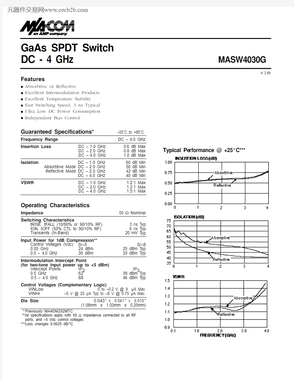
Insertion Loss
DC –1.0 GHz 0.6 dB Max DC –2.0 GHz 0.8 dB Max DC –4.0 GHz
1.0 dB Max Isolation
DC –
1.0 GHz 60 dB Min Absorbtive Mode DC –
2.0 GHz 50 dB Min Reflective Mode DC –
2.0 GHz 42 dB Min DC –
4.0 GHz
40 dB Min VSWR
DC –1.0 GHz 1.2:1 Max DC –2.0 GHz 1.2:1 Max DC –4.0 GHz
1.5:1 Max
Operating Characteristics
Impedance
50 ? Nominal Switching Characteristics
tRISE, tFALL (10/90% or 90/10% RF) 3 ns T yp
tON, tOFF (50% CTL to 90/10% RF) 6 ns T yp Transients (In-Band)20 mV T yp Input Power for 1dB Compression**
Control Voltages (Vdc)0/–50/–8
0.05 GHz 24 dBm 25 dBm T yp 0.5 – 4.0 GHz 30 dBm 33 dBm T yp
Intermodulation Intercept Point
(for two-tone input power up to +5 dBm)
Intercept Points IP 2IP 30.5 GHz 6239 dBm T yp 0.5 – 4.0 GHz 68
46 dBm T yp
Control Voltages (Complementary Logic)
VINLow 0 to –0.2 V @ 9 μA Max VINHi –5 V @ 25 μA T yp to –8 V @ 0.75 μA Max Die Size
0.043"x 0.041"x 0.010"
(1.08mm x 1.03mm x 0.25mm)
*Previously MA4GM202MTC
**All specifications apply with 50 ? impedance connected to all RF ports, and –5 Vdc control voltages.***Loss changes 0.0025 dB/°C
Features
q Absorbtive or Re?ective
q Excellent Intermodulation Products q Excellent Temperature Stability q Fast Switching Speed, 3 ns Typical q Ultra Low DC Power Consumption q
Independent Bias Control
Typical Pe r
formance @ +25°C***
元器件交易网https://www.360docs.net/doc/575185203.html,
V 2.00
Handling Precautions
Permanent damage to the MASW4030G may occur if the fol-lowing precautions are not adhered to:
A. Cleanliness —The MASW4030G should be handled in a clean environment. DO NOT attempt to clean unit after the MASW4030G is installed.
B. Static Sensitivity — All chip handling equipment and per-sonnel should be DC grounded.
C. Transient —Avoid instrument and power supply tran-sients while bias is applied to the MASW4030G. Use
shielded signal and bias cables to minimize inductive pick-up.D. Bias —Apply voltage to either of the complementary control ports only when the other is grounded. No port should be allowed to “float”.E. General Handling —It is recommended that the
MASW4030G chip be handled along the long side of the die with a sharp pair of bent tweezers. DO NOT touch the surface of the chip with fingers or tweezers.
Mounting
The MASW4030G is back-metallized with
Pd/Ni/Au(100/1,000/10,000?) metallization. It can be die-mounted with AuSn eutectic preforms or with thermally con-ductive epoxy. The package surface should be clean and flat before attachment.
Eutectic Die Attach:
A.A 80/20 gold/tin preform is recommended with a work surface temperature of approximately 255°C and a tool temperature of 265°C. When hot 90/10 nitrogen/hydrogen gas is applied, tool tip temperature should be approxi-mately 290°C.
B.DO NOT expose the MASW4030G to a temperature greater than 320°C for more than 20 seconds. No
more than 3 seconds of scrubbing should be required for attachment.Epoxy Die Attach:
A. Apply a minimum amount of epoxy and place the
MASW4030G into position. A thin epoxy fillet should be visible around the perimeter of the chip.B. Cure epoxy per manufacturer’s recommended schedule.C. Electrically conductive epoxy may be used but is not required.
H a n d l i n g ,Mounting and Bonding Pro c e d u r e MASW4030G
Wire Bonding
A.Ball or wedge with 1.0 mil diameter pure gold wire.
Thermosonic wirebonding with a nominal stage tempera-ture of 150°C and a ball bonding force of 40 to 50 grams or wedge bonding force of 18 to 22 grams is recommend-ed. Ultrasonic energy and time should be adjusted to the minimum levels achieve reliable wirebonds.
B.Wirebonds should be started on the chip and terminated on the package. GND bonds should be as short as possi-ble; at least three and no more than four bond wires from ground pads to package are recommended.
Schematic
元器件交易网https://www.360docs.net/doc/575185203.html,