Covalently Bound Hole-Injecting Nanostructures. Systematics of Molecular Architecture
Covalently Bound Hole-Injecting Nanostructures.Systematics of Molecular Architecture,Thickness,Saturation,and Electron-Blocking Characteristics on Organic Light-Emitting
Diode Luminance,Turn-on Voltage,and Quantum Efficiency Qinglan Huang,?Guennadi A.Evmenenko,?Pulak Dutta,?Paul Lee,§
Neal R.Armstrong,§and Tobin J.Marks*,?
Contribution from the Department of Chemistry and the Materials Research Center,and Department of Physics and Astronomy and the Materials Research Center,
Northwestern Uni V ersity,E V anston,Illinois60208,and Department of Chemistry and
Optical Science Center,Uni V ersity of Arizona,Tucson,Arizona85721
Received February19,2005;E-mail:t-marks@https://www.360docs.net/doc/5110458358.html,
Abstract:Hole transporting materials are widely used in multilayer organic and polymer light-emitting diodes (OLEDs,PLEDs,respectively)and are indispensable if device electroluminescent response and durability are to be truly optimized.This contribution analyzes the relative effects of tin-doped indium oxide(ITO) anode-hole transporting layer(HTL)contact versus the intrinsic HTL materials properties on OLED performance.Two siloxane-based HTL materials,N,N′-bis(p-trichlorosilylpropyl)-naphthalen-1-yl)-N,N′-diphenyl-biphenyl-4,4′-diamine(NPB-Si2)and4,4′-bis[(p-trichlorosilylpropylphenyl)phenylamino]biphenyl (TPD-Si2),are designed and synthesized.They have the same hole transporting triarylamine cores as conventional HTL materials such as1,4-bis(1-naphthylphenylamino)biphenyl(NPB)and N,N-diphenyl-N,N-bis(3-methylphenyl)-1,1-biphenyl)-4,4-diamine(TPD),respectively.However,they covalently bind to the ITO anode,forming anode-HTL contacts that are intrinsically different from those of the anode to TPD and NPB.Applied to archetypical tris(8-hydroxyquinolato)aluminum(III)(Alq)-based OLEDs as(1)the sole HTLs or(2)anode-NPB HTL interlayers,NPB-Si2and TPD-Si2enhance device electroluminescent response significantly versus comparable devices based on NPB alone.In the first case,OLEDs with36000cd/m2 luminance,1.6%forward external quantum efficiency(ηext),and5V turn-on voltages are achieved,affording a250%increase in luminance and~50%reduction in turn-on voltage,as compared to NPB-based devices. In the second case,even more dramatic enhancement is observed(64000cd/m2luminance;2.3%ηext; turn-on voltages as low as3.5V).The importance of the anode-HTL material contact is further explored by replacing NPB with saturated hydrocarbon siloxane monolayers that covalently bind to the anode,without sacrificing device performance(30000cd/m2luminance;2.0%ηext;4.0V turn-on voltage).These results suggest new strategies for developing OLED hole transporting structures.
1.Introduction
The past decade has witnessed the emergence of organic light-emitting diodes(OLEDs)as a practical display technology due to distinctive attractions such as low materials costs,self-emission,efficient and broad color tunability,compatibility with CMOS technology,and amenability to large-scale production.1-5 Improving OLED electroluminescent characteristics has been the focus of an extensive worldwide research effort that has led to appreciable fundamental understanding of the physical and chemical aspects of molecular solid-state electrolumines-cence(EL)and prototype devices with impressive perform-ance.6-13The mechanism of emission in OLEDs is now reasonably well understood and involves injection of electrons and holes from the cathode and anode,respectively,under application of an electric field.Some fraction of the electron-hole pairs recombine to form excitons,which in turn radiatively
?Department of Chemistry and the Materials Research Center,North-western University.
?Department of Physics and Astronomy and the Materials Research Center,Northwestern University.
§University of Arizona.
(1)For recent reviews of this subject,see:Veinot,J.G.C.;Marks,T.J.Acc.
Chem.Res.,in press.
(2)Chen,C.-T.Chem.Mater.2004,16,4389-4400.
(3)Nalwa,H.S.In Handbook of Ad V anced Electronic and Photonic Materials
and De V ices;Nalwa,H.S.,Ed.;Academic:San Diego,CA,2001;Vol.
10,pp1-51.
(4)Mitschke,U.;Bauerle,P.J.Mater.Chem.2000,10,1471-1507.
(5)Shim,H.-K.;Jin,J.-I.Ad V.Polym.Sci.2002,158,193-243.
(6)Niu,Y.H.;Hou,Q.;Cao,Y.Appl.Phys.Lett.2003,82,2163-2165.
(7)Duan,J.P.;Sun,P.P.;Cheng,C.H.Ad V.Mater.2003,15,224-227.
(8)Mller,C.D.;Falcou,A.;Reckefuss,N.;Rojahn,M.;Wiederhirn,V.;Rudati,
P.;Frohne,H.;Nuyken,O.;Becker,H.;Meerholz,K.Nature2003,421, 829-833.
(9)Niu,Y.H.;Yang,W.;Cao,Y.Appl.Phys.Lett.2002,81,2884-2886.
(10)Herguch,P.;Jiang,X.Z.;Liu,M.S.;Jen,A.K.Y.Macromolecules2002,
35,6094-6100.
(11)Lo,S.C.;Male,N.A.H.;Markham,J.P.J.;Magennis,S.W.;Burn,P.
L.;Salata,O.V.;Samuel,I.D.W.Ad V.Mater.2002,14,975-977. (12)Huang,Q.L.;Cui,J.;Veinot,J.G.C.;Yan,H.;Marks,T.J.Appl.Phys.
Lett.2003,82,331-333.
(13)D’Andrade,B.W.;Baldo,M.A.;Adachi,C.;Brooks,J.;Thompson,M.
E.;Forrest,S.R.Appl.Phys.Lett.2001,79,1045-
1047.
Published on Web06/30/2005
10.1021/ja051077w CCC:$30.25?2005American Chemical Society J.AM.CHEM.SOC.2005,127,10227-10242910227
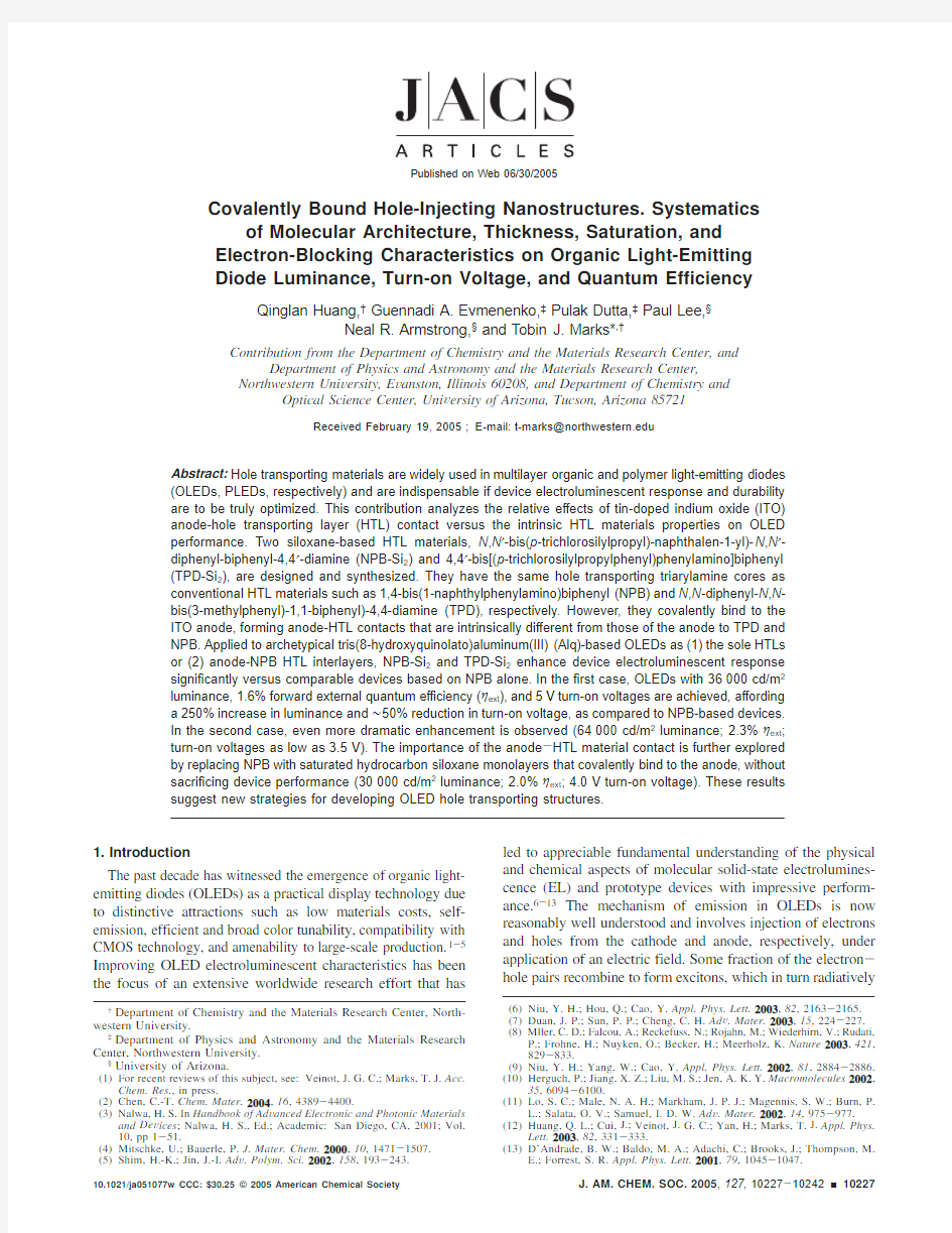
decay to ground states and emit light.4Sophisticated multilayer structures incorporating specifically tailored hole transport layers (HTLs),emissive layers (EMLs),and electron transport layers (ETLs)sandwiched between the two electrodes have been developed and generally exhibit superior device performance versus single-layer counterparts (Figure 1).To date,much effort has been devoted to developing new HTL materials to fulfill criteria such as substantial hole mobility,good energy level matching with anodes and EMLs (low hole injection barriers from the anode to the HTL and from the HTL to the EML;large electron injection barrier from the EML to the HTL),good thermal properties (stability;T g ),low optical absorption in the visible region,and smooth,amorphous film-forming mor-phology.14-22
To date,triarylamines have proven to be one of the most efficient classes of HTL molecules according to the above criteria,with 1,4-bis(phenyl-m -tolylamino)biphenyl (TPD,Scheme 1)an archetypical example.However,TPD has a low glass transition temperature (T g )65°C)and tends to crystallize at elevated temperatures,disrupting the amorphous nature of the HTL and causing device degradation.23Therefore,one major focus in developing HTL materials is to improve the poor thermal stability of TPD by synthesizing small molecule TPD analogues with higher T g parameters and/or by incorporating a triarylamine hole transport motif into a polymer chain.20,24,25In this regard,1,4-bis(1-naphthylphenylamino)biphenyl (NPB,Scheme 1)is a TPD analogue with a higher T g and has been widely used as a TPD replacement.26However,most of the effort in this direction has not led to significant device performance improvements over TPD-based OLEDs.In contrast,increasing evidence indicates that the anode (usually tin-doped
indium oxide,ITO)-HTL interface is crucial to hole injection in a common scenario where ITO -HTL contact rather than HTL bulk mobility limits charge injection.27-31A variety of interfacial engineering approaches have been applied to the anode -HTL junction,32-37including introduction of π-conjugated polymers,38copper phthalocyanine,26,39,40organic acids,41a thin layer of platinum,28self-assembled polar molecules 30,42or siloxanes,31,43and plasma treatment of the ITO surface.44All of these approaches have effects on hole injection and yield varying degrees of improved device performance in terms of turn-on voltage,luminance,stability,and/or quantum efficiency.How-ever,in general,the interlayers employed in these approaches cannot replace conventional triarylamine HTLs to yield high-performance OLEDs.Note that designing new HTL materials specifically targeting anode -HTL interfacial contact has largely been ignored.14,15,45
In this contribution,we present a full discussion of our efforts to design,synthesize,implement,and understand the conse-quences of hole transporting materials as OLED HTLs which achieve covalent ITO anode -HTL bonding (Scheme 2).46Followed by deposition of a conventional EML/ETL (tris(8-hydroxyquinolato)aluminum(III)(Alq,Scheme 1),this approach affords OLEDs with superior performance versus devices relying on simple ITO -NPB interfaces.For TPD-Si 2functionalized anodes,luminances as high as 36000cd/m 2with turn-on voltages as low as 5.0V are achieved,2.5×brighter and 4V lower,respectively,than for analogous NPB-based devices.Also,a current efficiency of ~6cd/A,equivalent to ~1.6%external forward quantum efficiency,is achieved at 12V.We also show that the same approach can be applied as covalently bonded ITO anode -NPB interlayers,resulting in OLEDs with more impressive performance (64000cd/m 2luminance;8cd/A
(14)Ren,X.;Alleyne,B.D.;Djurovich,P.I.;Adachi,C.;Tsyba,I.;Bau,R.;
Thompson,M.E.Inorg.Chem.2004,43,1697-1707.
(15)Hreha,R.D.;George,C.P.;Haldi,A.;Domercq,B.;Malagoli,M.;Barlow,
S.;Bredas,J.-l.;Kippelen,B.;Marder,S.R.Ad V .Funct.Mater.2003,13,967-973.
(16)Gong,X.;Moses,D.;Heeger,A.J.;Liu,S.;Jen,A.K.Y.Appl.Phys.
Lett.2003,83,183-185.
(17)Ma,C.-Q.;Zhang,L.-Q.;Zhou,J.-H.;Wang,X.-S.;Zhang,B.-W.;Cao,
Y.;Bugnon,P.;Schaer,M.;Nuesch,F.;Zhang,D.-Q.;Qiu,Y.Chin.J.Chem.2002,20,929-932.
(18)Fujikawa,H.;Ishii,M.;Tokito,I.;Taga,Y.Mater.Res.Soc.Symp.Proc.
2001,621,Q3.4.1-Q3.4.11.
(19)Liu,S.;Jiang,X.;Ma,H.;Liu,M.S.;Jen,A.K.Y.Macromolecules 2000,
33,3514-3517.
(20)Koene,B.E.;Loy,D.E.;Thompson,M.E.Chem.Mater.1998,10,2235-2250.
(21)Thayumanavan,S.;Barlow,S.;Marder,S.R.Chem.Mater.1997,9,3231-3235.
(22)Tang,C.W.;VanSlyke,S.A.Appl.Phys.Lett.1987,51,913-915.(23)Adachi,C.;Tsutsui,T.;Saito,S.Appl.Phys.Lett.1990,56,799-801.(24)Santerre,F.;Bedja,I.;Dodelet,J.P.;Sun,Y.;Lu,J.;Hay,A.S.;D’Iorio,
M.Chem.Mater.2001,13,1739-1745.
(25)Shirota,Y.;Okumoto,K.;Inada,H.Synth.Met.2000,111-112,387-391.
(26)Van Slyke,S.A.;Chen,C.H.;Tang,C.W.Appl.Phys.Lett.1996,69,
2160-2162.(27)Forsythe,E.W.;Abkowitz,M.A.;Gao,Y.J.Phys.Chem.B 2000,104,
3948-3952.
(28)Shen,Y.;Jacobs,D.B.;Malliaras,G.G.;Koley,G.;Spencer,M.G.;
Ioannidis,A.Ad V .Mater.2001,13,1234-1238.
(29)Nesch,F.;Forsythe,E.W.;Le,Q.T.;Gao,Y.;Rothberg,L.J.J.Appl.
Phys.2000,87,7973-7980.
(30)Appleyard,S.F.J.;Day,S.R.;Pickford,R.D.;Willis,M.R.J.Mater.
Chem.2000,10,169-173.
(31)Malinsky,J.E.;Jabbour,G.E.;Shaheen,S.E.;Anderson,J.D.;Richter,
A.G.;Marks,T.J.;Armstrong,N.R.;Kippelen,
B.;Dutta,P.;Peygham-barian,N.Ad V .Mater.1999,11,227-231.
(32)Zuppiroli,L.;Si-Ahmed,L.;Kamars,K.;Nesch,F.;Bussac,M.N.;Ades,
D.;Siove,A.;Moons,
E.;Grtzel,M.Eur.Phys.J.B 1999,11,505-512.(33)Ho,P.K.H.;Granstrom,M.;Friend,R.H.;Greenham,N.C.Ad V .Mater.
1998,10,769-771.
(34)Nesch,F.;Rtzinger,F.;Si-Ahmed,L.;Zuppiroli,L.Chem.Phys.Lett.1998,
288,861-867.
(35)Morgado,J.;Charas,A.;Barbagallo,N.;Alcacer,L.;Matos,M.;Cacialli,
F.Macromol.Symp.2004,212,381-386.
(36)Hatton,R.A.;Willis,M.R.;Chesters,M.A.;Rutten,F.J.M.;Briggs,D.
J.Mater.Chem.2003,13,38-43.
(37)Campbell,I.H.;Kress,J.D.;Martin,R.L.;Smith,D.L.;Barashkov,N.
N.;Ferraris,J.P.Appl.Phys.Lett.1997,71,3528-3530.
(38)Gross,M.;Muller,D.;Nothofer,H.;Scherf,U.;Neher,D.;Brauchle,C.;
Meerholz,K.Nature 2000,405,661-665.
(39)Tadayyon,S.M.;Grandin,H.M.;Griffiths,K.;Norton,P.R.;Aziz,H.;
Popovic,https://www.360docs.net/doc/5110458358.html,.Electron.2004,5,157-166.
(40)Mori,T.;Mitsuoka,T.;Ishii,M.;Fujikawa,H.;Taga,Y.Appl.Phys.Lett.
2002,80,3895-3897.
(41)Nesch,F.;Forsythe,E.W.;Le,Q.T.;Gao,Y.;Rothberg,L.J.J.Appl.
Phys.2000,87,7973-7976.
(42)Ganzorig,C.;Kwak,K.J.;Yagi,K.;Fujihira,M.Appl.Phys.Lett.2001,
79,272-274.
(43)Cui,J.;Huang,Q.;Wang,Q.;Marks,https://www.360docs.net/doc/5110458358.html,ngmuir 2001,17,2051-2054.
(44)Milliron,D.J.;Hill,I.G.;Shen,C.;Kahn,A.;Schwartz,J.J.Appl.Phys.
2000,87,572-576.
(45)Adachi,C.;Nagai,K.;Tamoto,N.Appl.Phys.Lett.1995,66,2679-2681.(46)Portions of this work were previously communicated in part.Huang,Q.;
Evmenenko,G.;Dutta,P.;Marks,T.J.J.Am.Chem.Soc.2003,125,14704-14705.Cui,J.;Huang,Q.;Veinot,J.C.G.;Yan,H.;Wang,Q.;Hutchison,G.R.;Richter,A.G.;Evmenenko,G.;Dutta,P.;Marks,https://www.360docs.net/doc/5110458358.html,ngmuir 2002,18,9958-
9970.
Figure 1.Cross-section of a typical multilayer OLED structure.
A R T I C L E S Huang et al.
10228J.AM.CHEM.SOC.
9
VOL.127,NO.29,2005
current efficiency at 10V;turn-on voltages as low as 3.5V).These anode functionalization processes are expected to sig-nificantly modify anode -HTL interfacial properties,47and here we discuss how these modifications translate into modified OLED EL device response.We also present here evidence that simple saturated hydrocarbon self-assembled monolayers (SAMs;Scheme 2)can function as HTLs and ITO -NPB interlayers,affording a better understanding of silane-anode modification effects.Devices with luminances as high as 30000cd/m 2and current efficiencies of ~7cd/A,equivalent to ~2%external forward quantum efficiency,at 7.0V can be achieved.Taken together,these results require some reassessment of current HTL structure -function models.
2.Experimental Section
Materials and Methods.ITO glass sheets (20?/0,rms roughness ) 2.5nm)were purchased from Colorado Concept Coating.All chemical reagents were used as received unless otherwise indicated.All manipulations of air/moisture-sensitive materials were carried out on a dual-manifold Schlenk line or in a nitrogen-filled glovebox.Ether and THF were distilled before use from sodium/benzophenone ketyl.Methylene chloride was distilled before use from calcium hydride.Toluene was dried using activated alumina and Q5columns and tested with benzyphenone ketyl in ether solution.TPD and Alq were purchased
from Sigma-Aldrich and purified via vacuum gradient sublimation.The OLED component,2,9-dimethyl-4,7-diphenyl-1,10-phenanthroline (BCP,Scheme 1),was purchased from Fluka and purified via vacuum gradient sublimation.NPB was synthesized according to the literature 20and was purified by recrystallization followed by vacuum gradient sublimation.N ,N ′-Di(3-heptyl)quinacridone (DIQA,Scheme 1)was synthesized and purified according to the literature.48NMR spectra were obtained on Varian VXR-400or 500MHz NMR instruments.MS analyses were conducted on a Micromass Quattro II Triple Quadrupole HPLC/MS/MS mass spectrometer.Elemental analyses were carried out by Midwest Microlabs.Cyclic voltammetry was performed with a BAS 100electrochemical workstation (SAM-coated ITO with ~1cm 2area working electrodes,Ag wire pseudo-reference electrode,Pt wire counter electrode,0.1M TBAHFP in anhydrous MeCN supporting electrolyte,and 0.001M ferrocene as the internal pinhole probe;scan rate )0.1V/s).TBAHFP was recrystallized from an ethyl acetate/hexanes mixture and dried in vacuo at 100°C for 10h.Ferrocene was purchased from Sigma-Aldrich and purified via vacuum gradient sublimation.IR spectra were obtained on a Bio-Rad FTS-40FTIR spectrometer.AFM images were obtained on a Nanoscope III AFM under ambient conditions in the contact mode with Si 3N 4cantilevers.Specular X-ray reflectivity experiments on coated single-crystal Si (111)or Si (100)substrates were performed on the Naval Research Laboratory X23B beamline at the National Synchrotron Light Source.Data were acquired and analyzed as described previously.46The thickness of spin-cast films was measured with a Tencor P-10profilometer.Ultraviolet photoelec-tron spectroscopy (UPS)experiments on TPD-Si 2and NPB-Si 2SAM-coated ITO substrates were carried out at the University of Arizona using the 21.2eV He (I)source (Omicron H15-13)of a Kratos Axis-165Ultra photoelectron spectrometer.HOMO values were estimated from the median energy of the clearly defined photoionization peak,while IP values were estimated from the extrapolation of the high kinetic energy edge of that peak to zero intensity.
Synthesis of 4,4′-Bis[(p -bromophenyl)phenylamino)]biphenyl (1).To a toluene solution (50mL)of tris(dibenzyldeneacetone)dipalladium (0.55g,0.60mmol)and bis(diphenylphosphino)ferrocene (0.50g,0.90mmol)was added 1,4-dibromobenzene (18.9g,0.0800mol)at 25°C.Following stirring under an N 2atmosphere for 10min,sodium tert -butoxide (4.8g,0.050mol)and N ,N ′-diphenylbenzidine (6.8g,0.020mol)were added.The reaction mixture was then stirred at 90°C for 12h,followed by cooling to 25°C.The reaction mixture was then poured into water,and the organic and aqueous layers were separated.The aqueous layer was extracted with toluene (3×100mL),and the
(47)Cahen,D.;Hodes,G.Ad V .Mater.2002,14,789-798.
(48)Shaheen,S.E.;Kippelen,B.;Peyghambarian,N.;Wang,J.F.;Anderson,
J.D.;Mash,E.A.;Lee,P.A.;Armstrong,N.R.;Kawabe,Y.J.Appl.Phys.1999,85,7939-7945.
Scheme 1.Structures of Multilayer OLED Constituent Materials:TPD,NPB,and PEDOT(HTL),Alq (EML/ETL),DIQA(EML Dopant),and BCP
(ETL)
Scheme 2.Chemical Structures of the Organosiloxanes Used as HTLs and ITO Anode Modification
Layers
Covalently Bound Hole-Injecting Nanostructures A R T I C L E S
J.AM.CHEM.SOC.
9
VOL.127,NO.29,200510229
resulting extracts were combined with the original organic layer.The solvent was removed in vacuo giving a crude product which was purified by chromatography on a silica gel column(6:1hexane:ethylene chloride eluent)to yield pure1as a colorless solid(6.9g)in50% yield.1H NMR(CDCl3):δ6.99(d,J)8.8Hz,4H),7.02-7.16(m, 10H),7.28(t,J)7.6Hz,4H),7.34(d,J)8.8Hz,4H),7.45(d,J) 8.4Hz,4H).
Synthesis of4,4′-Bis[(p-allylphenyl)phenylamino]biphenyl(2). Using standard Schlenk techniques,1.6mL(3.5mmol)of n-butyl-lithium(2.5M in hexanes)was added dropwise under inert atmosphere to an ether solution(10mL)of1(1.02g,1.58mmol)while maintaining the temperature at25°C.The mixture was stirred for2h,after which time CuI(0.76g,4.0mmol)was added.Upon cooling the reaction mixture to0°C,allyl bromide(0.60g,5.0mmol)was added in one portion,and the mixture was stirred for14h,followed by quenching with saturated aqueous NH4Cl solution(100mL)and extraction with ether(3×100mL).The combined ether extracts were washed with water(2×100mL)and brine(2×100mL),and dried over anhydrous Na2SO4.Filtration and removal of solvent in vacuo afforded a yellow oil,which was further purified by chromatography on a silica gel column(4:1hexane:methylene chloride)to yield0.63g of pure2as a colorless solid.Yield,70%.1H NMR(CDCl3):δ3.40(d,J)10Hz, 4H),5.10-5.20(m,4H),6.02(m,2H),6.99-7.10(m,2H),7.10-7.20(m,16H),7.28(t,J)7.6Hz,4H),7.46(d,J)8.8Hz,4H). Anal.Calcd for C42H36N2:C,88.68;H,6.39;N,5.23.Found:C,87.50; H,6.35;N,4.93.
Synthesis of4,4′-Bis[(p-trichlorosilylpropylphenyl)phenylamino]-biphenyl(TPD-Si2,3).Under inert atmosphere at25°C,a grain of H2PtCl6?n H2O,followed by HSiCl3(0.73g,5.5mmol),was added to a CH2Cl2solution(30mL)of2(0.32g,0.55mol),and the reaction mixture was stirred at30°C for4h.Removal of the solvent in vacuo yielded a dark-yellow oil,which was triturated with a mixture of50 mL of pentane and10mL of toluene to yield a solid that was removed by filtration.The filtrate was concentrated in vacuo to yield3as a viscous,pale-yellow oil.Yield,98%.1H NMR(CDCl3):δ1.45(t,J )7Hz,4H),1.90(t,J)7Hz,4H),2.70(brs,4H),6.80-7.80(m, 26H).Anal.Calcd for C42H38Cl6N2Si2:C,60.07;H,4.57.Found:C, 60.52;H,4.87.
Synthesis of N,N′-Bis(p-bromonaphthalen-1-yl)-N,N′-diphenyl-biphenyl-4,4′-diamine(4).To a toluene solution(50mL)of tris-(dibenzylideneacetone)dipalladium(0.048g,0.052mmol)and bis-(diphenylphosphino)ferrocene(0.044g,0.079mmol)was added1,4-dibromonaphathelene(1.0g,3.5mmol)at25°C.Following stirring under an N2atmosphere for10min,sodium tert-butoxide(0.34g,3.5 mmol)and N,N′-diphenylbenzidine(0.47g,1.4mmol,purified by sublimation)were added.The reaction mixture was stirred at90°C for22h,followed by cooling to25°C.The reaction mixture was then poured into water,and the organic and aqueous layers were separated. The aqueous layer was extracted with toluene(3×100mL),and the resulting extracts were combined with the original organic layer.The solvent was removed in vacuo giving a crude product that was purified by chromatography on a silica gel column(6:1hexane:methylene chloride eluent)to yield pure4as a colorless solid(0.20g)in20% yield.1H NMR(CDCl3):δ6.96-7.05(m,10H),7.19-7.23(m,6H), 7.36-7.42(m,4H),7.57(t,J)8.5Hz,4H),7.77(d,J)9.5Hz, 2H),7.98(d,J)10.5Hz,2H),8.27(d,J)10.5Hz,2H).
Synthesis of N,N′-Bis(p-allylnaphthalen-1-yl)-N,N′-diphenyl-bi-phenyl-4,4′-diamine(5).To a stirring,anhydrous THF solution(10 mL)of4(0.10g,0.13mmol)under inert atmosphere was added dropwise at-78°C n-butyllithium(1.6M in hexanes,0.17mL,0.27 mmol),and the mixture was stirred for15min.Copper iodide(I)(0.051 g,0.27mmol)was then added.After the mixture was stirred for5 min,allyl bromide(0.07g,0.54mmol)was added in one portion.The solution was gradually warmed to25°C and stirred for2h,after which time it was quenched with100mL of saturated aqueous NH4+Cl-solution,followed by extraction with ether(3×100mL).The combined ether extracts were washed with water(2×100mL)and brine(2×100mL),and dried over anhydrous Na2SO4.Following filtration,the solvent was removed in a vacuum to yield an oil.Chromatography on silica gel with hexane:methylene chloride(10:1)afforded0.070g of5 as a colorless solid.Yield,80%.1H NMR(CDCl3):δ3.90(d,J)4.5 Hz,4H),5.17-5.20(m,4H),6.20(m,2H),6.95(t,J)7.5Hz,2H), 7.06-7.10(m,10H),7.21-7.24(m,4H),7.30(d,J)7.5Hz,2H),
7.37-7.40(m,8H),7.50-7.53(m,2H),8.04(d,J)8.0Hz,2H),
8.09(d,J)9.0Hz,2H).MS(m/z):669.2[M,100].Anal.Calcd for C50H40N2:C,89.77;H,6.04;N,4.19.Found:C,89.54;H,6.04;N, 4.21.
Synthesis of N,N′-Bis(p-trichlorosilylpropyl)-naphthalen-1-yl)-N,N′-diphenyl-biphenyl-4,4′-diamine(NPB-Si2,6).To a solution of 5(0.040g,0.060mmol)in25mL of dry toluene at25°C under inert atmosphere was added H2PtCl6?n H2O(0.001g),followed by trichlo-rosilane(0.060mL,0.60mmol).The reaction solution was warmed to 50°C and monitored by NMR until the completion of reaction.Re-moval of the solvent in a vacuum yielded an oil.Next,20mL of dry toluene was added to the residue and the resulting solution was filtered into a Schlenk flask by cannula.The filtrate was concentrated under vacuum to give6as a pale-yellow oil.Yield,98%.1H NMR(CDCl3):δ1.70(t,J)6.0Hz,4H),2.10(t,J)7Hz,4H),3.21(t,J)7Hz, 4H),6.94(m,2H),7.03-7.07(m,10H),7.19-7.22(m,4H),7.33-7.40(m,8H),7.50-7.53(m,2H),7.54(d,J)8.0Hz,2H),7.72(d, J)9.0Hz,2H),8.04(d,J)9.0Hz,2H).Anal.Calcd for C50H42Cl6N2Si2:C,63.90;H,4.50;N,2.98.Found:C,63.54;H,4.04; N,2.90.
Self-Assembly of TPD-Si2and NPB-Si2on ITO Substrates.ITO substrates were cleaned in an ultrasonic detergent bath,followed by methanol,2-propanol,and finally acetone.The substrates were subse-quently treated in an oxygen plasma cleaner for1min to remove any residual organic contaminants.Following strict Schlenk protocol,clean ITO substrates were immersed in a1.0mM dry toluene solution of TPD-Si2or NPB-Si2,respectively.After heating at~80°C for1h,the toluene solution was removed by cannula and the substrates were rinsed with dry toluene(2×50mL)and wet acetone,followed by transferring to a120°C oven for1h to expedite cross-linking.Longer thermal curing yields films with similar properties,and the coating procedure has negligible effects on the measured sheet resistance of the underlying ITO.
Self-Assembly of TPD-Si2and NPB-Si2on Silicon Substrates. Silicon(111)or(100)substrates(Semiconductor Processing Co.)were subjected to a cleaning procedure as follows:immersion in“piranha”solution(concentrated H2SO4:30%H2O2;70:30v/v)at80°C for1h. After being cooled to room temperature,substrates were rinsed repeatedly with deionized(DI)water followed by an RCA-type cleaning protocol(H2O:30%H2O2:NH3;5:1:1v/v/v;sonicated at room temper-ature for40min).The substrates were finally rinsed with copious amounts of DI water,heated to125°C for15min,and dried in vacuo. TPD-Si2and NPB-Si2were then self-assembled onto the clean silicon substrates following the procedure described above for ITO substrates.
Spin-Casting TPD-Si2and NPB-Si2on ITO Substrates.Dry toluene solutions of TPD-Si2or NPB-Si2(10mg/mL)were spin-coated onto clean ITO surfaces at2krpm in air,followed by curing in a vacuum oven at110°C for1h.
Fabrication of OLED Devices.All OLED devices were fabricated on bare ITO substrates that were treated with solvents and an oxygen plasma,as described previously,or on TPD-Si2/NPB-Si2modified ITO substrates.The substrates were loaded into a bell jar deposition chamber housed in a nitrogen-filled glovebox.A typical deposition procedure is as follows:at1×10-6Torr,a20nm layer of NPB was first de-posited,followed by60nm of Alq doped with1%DIQA.Both organic layers were grown at a deposition rate of2-3?/s.Another20nm thick layer of BCP was then deposited,followed by thermally evap-orating1nm thick Li.Finally,a100nm thick Al cathode was deposited through a shadow mask.This metallic layer was patterned via a shadow
A R T I C L E S Huang et al. 10230J.AM.CHEM.SOC.9VOL.127,NO.29,2005
mask to give four devices,each with an area of 0.10cm 2.OLED device characterization was carried out with a computer-controlled Keithley 2400source meter and IL 1700research radiometer equipped with a calibrated silicon photodetector at 25°C under ambient atmosphere.External quantum efficiency was estimated from current density versus voltage and luminance versus current density characteristics.
Fabrication of Hole-Only Devices.All hole-only devices were fabricated on bare ITO substrates that were treated with solvents and an oxygen plasma,as described previously,or on TPD-Si 2/NPB-Si 2modified ITO substrates.The substrates were loaded into a bell jar deposition chamber housed within a nitrogen-filled glovebox.At a base pressure of 1×10⁻⁶Torr,NPB (400nm)was vapor deposited at a rate of ~3?/s,followed by sputter-coating of a 6nm of Au layer through the same shadow mask employed for OLED fabrication de-scribed above.Single-carrier device assembly was subsequently com-pleted with the masked thermal vapor deposition of Al (150nm).Device behavior was evaluated using the computer-controlled Keithley 2400sourcemeter.
3.Results
In Section 3.1,we report the deposition and characterization of TPD-Si 2and NPB-Si 2on ITO or Si substrates.In Section 3.2,spin-coated or self-assembled TPD-Si 2and NPB-Si 2layers replace the conventional vapor-deposited NPB layer in Alq-based OLEDs.Their current/luminous functions as new types of covalently bonded HTLs are described.Alternatively,TPD-Si 2and NPB-Si 2are used as ITO anode -NPB interlayers,and the effect on OLED EL response is analyzed here.In Section 3.3,alkylsiloxane SAMs are employed as HTLs and ITO -NPB interlayers,and the effect on device performance is compared to that of the above triarylaminesiloxanes.
3.1.Deposition and Characterization of TPD-Si 2and NPB-Si 2on ITO or Silicon Substrates.The synthetic pathways to TPD-Si 2and NPB-Si 2are summarized in Scheme 3,while detailed procedures and characterization data are presented in the Experimental Section.Utilizing a self-limiting,solution-based chemisorption process,TPD-Si 2and NPB-Si 2are self-assembled onto hydrophilic ITO substrate surfaces with nano-precise control in thickness.As illustrated in Scheme 4,clean ITO-coated glass or single-crystal silicon surfaces possess hydroxyl functionalities and adsorbed water,which are reactive toward chlorosilanes,thereby affording covalent binding of the
silanes to the surface.49-52Further exposure to air and moisture in the following wet acetone rinse in air hydrolyzes any unreacted trichlorosilyl groups.Thermal curing facilitates the formation of cross-linked siloxane networks,resulting in a thin layer consisting of hole transporting motifs covalently anchored to the ITO or Si surface.At completion of the silane condensa-tion,chlorine concentrations in the film are below XPS detection limits.53,54The microstructural characterization of these layers is presented below.Spin-casting TPD-Si 2and NPB-Si 2from hydrocarbon solutions onto ITO or Si substrates affords thicker (~40nm)films on these substrates,following chemistry similar to that described above,given that the spin-coating parameters such as solution concentration and spinning speed are carefully controlled (see Experimental Section for details).
Characterization of TPD-Si 2and NPB-Si 2Siloxane Films by Specular X-ray Reflectivity Measurements.Specular X-ray reflectivity (XRR)measurements were performed upon the films deposited on cleaned single-crystal Si(111)or Si (100)surfaces,using the self-assembly procedure discussed above.Fitting of the X-ray reflectivity data,normalized to the Fresnel reflectivity,to a physically reasonable model provides details of the film thickness,smoothness,interfacial abruptness,and density.In general,the reflectivity can be expressed in terms of the average electron density by eqs 1and 2,55
where R F is the theoretical Fresnel reflectivity for a smooth interface,k z is the momentum transferred (k z )4π/λsin θ),d ?F ?/d z is the derivative of the electron density along the surface normal direction,averaged over the in-plane coherence length of the X-rays,and F ∞is the electron density of the substrate (Si).By fitting the XRR data for the self-assembled TPD-Si 2and NPB-Si 2films on Si,the thickness,electron density,and roughness were determined.These data are compiled in Table 1.
Characterization of Self-Assembled TPD-Si 2and NPB-Si 2Monolayers by Ultraviolet Photoelectron Spec-troscopy (UPS).UPS measurements were conducted on ITO surfaces covered with TPD-Si 2and NPB-Si 2SAMs.The bare ITO surface,which had been Ar +-sputtered in vacuo,is used
(49)Ulman,A.Chem.Re V .1996,96,1533-1554.
(50)Jeon,N.L.;Nuzzo,R.G.;Xia,Y.;Mrksich,M.;Whitesides,G.M.
Langmuir 1995,11,3024-3026.
(51)Ulman,A.Thin Solid Films 1996,273,48-53.
(52)Woodward,J.T.;Ulman,A.;Schwartz,https://www.360docs.net/doc/5110458358.html,ngmuir 1996,12,3626-3629.
(53)Donley,C.;Dunphy,D.;Paine,D.;Carter,C.;Nebesny,K.;Lee,P.;
Alloway,D.;Armstrong,https://www.360docs.net/doc/5110458358.html,ngmuir 2002,18,450-457.
(54)Malinsky,J.E.;Veinot,J.C.G.;Jabbour,G.E.;Shaheen,S.E.;Anderson,
J.D.;Lee,P.;Richter,A.G.;Burin,A.L.;Ratner,M.A.;Marks,T.J.;Armstrong,N.R.;Kippelen,B.;Dutta,P.;Peyghambarian,N.Chem.Mater.2001,14,3054-3065.
(55)Richter,A.G.;Yu,C.J.;Datta,A.;Kmetko,J.;Dutta,P.Phys.Re V .E
2000,61,607-615.
Scheme 3.Synthesis of TPD-Si 2and NPB-Si
2
Scheme 4.Scheme for ITO Surface Modified by Covalently Bound HTL
Materials
R (k z ))R F (k z )|Φ(k z )|2(1)Φ(k z ))
∫1F ∞
d ?F ?d z
e ik z z
d z (2)
Covalently Bound Hole-Injecting Nanostructures
A R T I C L E S
J.AM.CHEM.SOC.
9
VOL.127,NO.29,200510231
as reference for the low kinetic energy edge of the photoemission spectrum in the measurement.A 0.1eV shift in the low kinetic energy edge of the photoemission spectrum obtained from the analysis of the SAM-covered ITO surface is observed for both TPD-Si 2and NPB-Si 2,indicating interfacial dipole for-mation.56The sign of the vacuum level shift for the TPD-Si 2SAMs is uncertain due to experimental errors.Estimates of the effective surface work function can be obtained from the measured width of the UV-photoemission spectrum,subtracted from the source energy,using the high and low kinetic energy edges of the photoemission spectra.The analysis shows nearly identical HOMO and IP values for TPD-Si 2and NPB-Si 2SAM modified ITO surfaces (5.2and 5.4eV,respectively,Table 2).
Characterization of TPD-Si 2and NPB-Si 2Siloxane Films by Atomic Force Microscopy.Contact mode AFM imaging was carried out on three spots randomly chosen on self-assembled or spin-cast TPD-Si 2or NPB-Si 2covered ITO substrates,respectively.Uniform films with no evidence of cracks or pinholes were observed over a 5×5μm scan area (Figure 2).The rms roughness is 1.39and 3.18nm,respectively,for TPD-Si 2and NPB-Si 2SAMs,and 0.79and 3.43nm,respectively,for spin-coated TPD-Si 2and NPB-Si 2films,as compared to bare ITO substrates with an rms roughness of 2.5nm.
Characterization of TPD-Si 2and NPB-Si 2Siloxane Films by Cyclic Voltammetry.TPD-Si 2and NPB-Si 2SAM-coated ITO,silver wire,and Pt wire were used as the working elec-trode,reference electrode,and counter electrode,respectively,in 0.1M acetonitrile solution of tetrabutylammonium hexa-fluorophosphate as the electrolyte without the ferrocene.Inte-gration of the oxidation peak areas and assuming two elec-tron oxidation/reduction events per molecular unit yields surface coverages of 2.5×10⁻¹⁰mol/cm 2(TPD-Si 2SAM)and 2.2×10⁻¹⁰mol/cm 2(NPB-Si 2SAM),respectively.57Analo-gously,a close-packed monolayer of ferrocene dicarboxylic acid absorbed on ITO yields 4.0×10⁻¹⁰mol/cm 2surface coverage.53
To examine the present HTL SAMs for pinholes over the entire ITO substrate area,cyclic voltammetry experiments using ferrocene as a redox probe were then carried out.58Here,TPD-Si 2or NPB-Si 2SAM-coated ITO substrates were used as working electrodes.Bare ITO substrates were used as references to calibrate the ferrocene redox potential for each measurement.It was observed that the ferrocene oxidation potential shifts from 0.59V,as shown in Figure 3,when bare ITO substrates are used as working electrodes,to 0.84and 0.77V,respectively,for the TPD-Si 2and NPB-Si 2SAM-covered ITO substrates as working electrodes.It is expected that the pinhole-free films of TPD-Si 2and NPB-Si 2SAMs on ITO electrodes will block the oxidation of solution ferrocene,until potentials are reached where the bis-trarylamine groups are oxidized,providing sites for mediated oxidation of solution phase ferrocene.59,60For both TPD-Si 2and NPB-Si 2SAMs on ITO,the peak potential for oxidation of ferrocene is indeed shifted positively by ca.0.2V.The reduction of the ferricenium cation on the return sweep is partially blocked by the NPB-Si 2layer,and more completely blocked by the TPD-Si 2layer,suggesting that the latter SAM layer is somewhat more pinhole free.61The larger separations of ferrocene oxidative and reductive peak potentials at the SAM-coated ITO electrodes versus on the bare ITO ones
(56)Ishii,H.;Sugiyama,K.;Ito,E.;Seki,K.Ad V .Mater.1999,11,605-625.(57)Murray,R.W.In Molecular Design of Electrode Surfaces,Techniques of
Chemistry ;Murray,R.W.,Ed.;Wiley:New York,1992;Vol.22,pp 1-158.
(58)DuBois,C.J.,Jr.;McCarley,R.L.J.Electroanal.Chem.1998,454,99-105.
(59)Immoos,C.E.;Chou,J.;Bayachou,M.;Blair,E.;Greaves,J.;Farmer,P.
J.J.Am.Chem.Soc.2004,126,4934-4942.
(60)Nowall,W.B.;Kuhr,W.G.Anal.Chem.1995,67,3583-3588.
(61)Inzelt,G.In Electroanalytical Chemistry ;Bard,A.J.,Rubenstein,I.,Eds.;
Marcel Dekker:New York,1994;Vol.18,pp 90-134.
Table 1.XRR-Derived Electron Density,Roughness,and Thickness Data for Self-Assembled TPD-Si 2and NPB-Si 2Monolayers on Si (100)Substrates
monolayer
electron density
(e ?-3)
roughness (?)
thickness (?)
TPD-Si 20.32-0.357.8(0.217.8(0.2NPB-Si 20.45-0.47 4.1(0.214.1(0.2
Table 2.UPS Measured Ionization Potential,Highest Occupied Molecular Orbital (HOMO)Energy,and Vacuum Level Shift for TPDSi 2and NPBSi 2Self-Assembled Monolayers on ITO Substrates
ionization potential (eV)
HOMO (eV)
vacuum level shift (eV)
TPD-Si 2 5.2 6.1(0.1NPB-Si 2 5.4 6.1-
0.1
Figure 2.Tapping mode AFM images of self-assembled and spin-cast TPD-Si 2and NPB-Si 2films on ITO substrates.(A)TPD-Si 2SAM on ITO.RMS roughness )1.39nm.(B)TPD-Si 2spin coated film on ITO.RMS roughness )0.79nm.(C)NPB-Si 2SAM on ITO.RMS roughness )3.18nm.(D)NPB-Si 2spin coated film on ITO.RMS roughness )3.43
nm.Figure 3.Cyclic voltammetry characteristics of self-assembled TPD-Si 2and NPB-Si 2monolayer films on an ITO electrode immersed in a ferrocene solution.Electrolyte:0.1M TBAHFP in anhydrous MeCN.Sweep speed:0.1V/s.
A R T I C L E S
Huang et al.
10232J.AM.CHEM.SOC.
9
VOL.127,NO.29,2005
(1.68V,TPD-Si2SAM;0.86V,NPB-Si2SAM;0.30V,bare ITO)may also indicate that in the redox processes,counterion penetration and diffusion in the SAMs are retarded,presumably due to the densely packed,cross-linked SAM networks.62-65It is likely that TPD-Si2,due to its smaller core triarylamine molecular volume,encounters less steric hindrance in the film-forming intermolecular cross-linking process as compared to NPB-Si2,resulting in more densely packed films.The more distorted curve shape for the TPD-Si2SAM is presumably related to its more densely packed,cross-linked coverage and differentπ-system redox kinetics versus NPB-Si2.
3.2.Self-Assembled and Spin-Cast TPD-Si2and NPB-Si2 Films in OLEDs.Replacing NPB with TPD-Si2and NPB-Si2SAMs in OLEDs.Alq-based OLEDs having the structure ITO anode/HTL/Alq doped with DIQA/BCP doped with Li/Al were fabricated to study the function of TPD-Si2 and NPB-Si2films as HTLs.Replacing vapor-deposited con-ventional20nm thick NPB HTLs with nanometer-scale thick SAMs of TPD-Si2or NPB-Si2in the above OLEDs was first investigated,and EL response data are shown in Figure
4.Note that the OLEDs exhibit greater luminance and,in some regimes, higher external quantum efficiencies when the conventional20 nm thick HTL(NPB)is replaced with~2nm thick TPD-Si2 and NPB-Si2SAMs.The maximum luminance is~18000cd/ m2(NPB-Si2),~17000cd/m2(TPD-Si2),and~14000cd/m2 (NPB-only).Also,the NPB-Si2and TPD-Si2SAM-based OLEDs have lower turn-on and operating voltages.For instance, the operating voltage at300cd/m2,a standard brightness for displays,is8.0,8.5,and10.5V for NPB-Si2,TPD-Si2,and NPB-only,respectively.However,the maximum external forward quantum efficiencies are0.8%(NPB-Si2),0.75% (TPD-Si2),and1.87%(NPB-only).OLEDs without HTLs were also fabricated here as a comparison,and the dramatic effects on device performance induced by the SAMs are clearly evident (Figure4).
Replacing Conventional HTLs with Spin-Cast TPD-Si2 and NPB-Si2Films in OLEDs.TPD-Si2and NPB-Si2were spin-coated onto ITO substrates and thermally cured in a vacuum oven at110°C for1h,yielding films with a thickness of~40 nm,as measured by profilometry,followed by vapor-deposition of Alq doped with DIQA,then BCP,Li,and Al.Again,
replacing NPB with the cross-linked siloxane films results in higher luminance and external quantum efficiencies at identical bias(Figure5).The maximum luminance achieved is~23000 cd/m2(NPB-Si2),~36000cd/m2(TPD-Si2),and~14000 cd/m2(NPB-only).Maximum forward external quantum ef-ficiencies are0.8%(NPB-Si2),1.6%(TPD-Si2),and1.87% (NPB-only).The operating bias for300cd/m2is7.0,7.0,and 10.5V for NPB-Si2,TPD-Si2,and NPB-only,respectively.In Table3,the EL response data are compared among devices using NPB-Si2and TPD-Si2SAMs,spin-cast NPB-Si2and TPD-Si2films,and NPB-only as the HTL,respectively.OLEDs with spin-cast TPD-Si2films as the HTL exhibit more than a2-fold increase of maximum luminance,~50%lower turn-on voltage, and comparable external forward quantum efficiency versus those of devices having NPB only as the HTL.
Applying TPD-Si2and NPB-Si2SAMs as ITO Anode-NPB Interlayers.OLED EL Response.Self-assembled TPD-Si2and NPB-Si2films can also be applied as interlayers between the ITO anode and the conventional NPB HTL in OLEDs having structures ITO anode/SAM/NPB/Alq doped with DIQA/BCP/Li/Al.Insertion of these interlayers between the anode and the NPB HTL dramatically enhances OLED EL response as compared to devices without the interlayers(Figure 6).As compared to OLEDs using TPD-Si2or NPB-Si2SAMs as the HTLs,which are directly in contact with the EML(Figure 4),the maximum light output is enhanced by a factor of~3×both for TPD-Si2-and for NPB-Si2-based devices:~18000 cd/m2f50000cd/m2(NPB-Si2/NPB),~17000cd/m2f 45000cd/m2(TPD-Si2/NPB).Likewise,the maximum forward external quantum efficiency is increased to1.8%(NPB-Si2/NPB) and 2.3%(TPD-Si2/NPB)versus0.8%(NPB-Si2),0.75% (TPD-Si2),and1.87%(NPB alone).
(62)Napper,A.M.;Liu,H.Y.;Waldeck,D.H.J.Phys.Chem.B2001,105,
7699-7707.
(63)Nahir,T.M.;Clark,R.A.;Bowden,E.F.Anal.Chem.1994,66,2595-
2598.
(64)Forster,R.J.Inorg.Chem.1996,35,3394-3403.(65)Richardson,J.N.;Rowe,G.K.;Carter,M.T.;Tender,L.M.;Curtin,L.
S.;Peck,S.R.;Murray,R.W.Electrochim.Acta1995,40,1331-
1338. Figure4.Responses of OLEDs having structures ITO/HTL/Alq:1%DIQA (60nm)/BCP:Li(20nm)/Al(100nm),HTL)NPB-Si2SAM(1.4nm), TPD-Si2SAM(1.7nm),NPB(20nm)only.(A)Current density versus voltage;(B)luminance versus voltage;(C)external forward quantum efficiency versus voltage.
Covalently Bound Hole-Injecting Nanostructures A R T I C L E S
J.AM.CHEM.SOC.9VOL.127,NO.29,200510233
Spin-Cast TPD-Si 2and NPB-Si 2Films as ITO Anode -NPB Interlayers.OLED EL Response.Spin-casting TPD-Si 2or NPB-Si 2layers onto ITO anodes,followed by vapor-depo-sition of NPB,was also investigated as an alternative approach to applying these silanes as the anode -NPB interlayers.Again,improved EL response is observed versus that of OLEDs with-out interlayers and versus devices fabricated with only spin-coated films as HTLs (Figure 7):maximum light output,~46000cd/m 2(NPB-Si 2/NPB),~64000cd/m 2(TPD-Si 2/NPB)versus ~23000cd/m 2(NPB-Si 2),~36000cd/m 2(TPD-Si 2),~14000cd/m 2(NPB-only);maximum forward external quan-tum efficiencies,2.4%(NPB-Si 2/NPB),2.3%(TPD-Si 2/NPB)versus 0.8%(NPB-Si 2),1.6%(TPD-Si 2),1.87%(NPB-only);turn-on voltages,4.0V (NPB-Si 2/NPB),6V (TPD-Si 2/NPB)versus 5.0V (NPB-Si 2),5.0V (TPD-Si 2),9.0V (NPB-only).In Table 4,the EL response data are compared for devices using NPB-Si 2and TPD-Si 2SAMs,as well as spin-cast NPB-Si 2and TPD-Si 2films as ITO anode -NPB interlayers,respectively.Hole-Only Devices.Hole-only devices were fabricated to investigate the effect of NPB-Si 2and TPD-Si 2SAM coatings
on hole injection efficiency from the ITO anode into the NPB HTL.65I -V characteristics were measured on devices having structure ITO/siloxane/NPB(400nm)/Au (6nm)/Al (Figure 8).Orders of magnitude larger hole currents are observed for devices with the siloxane SAMs as ITO anode -NPB interlayers,indicating strong hole injection enhancement by modifying the anode with NPB-Si 2and TPD-Si 2,respectively.Attempting to measure hole fluence through either the self-assembled or the spin-coated siloxane films in ITO/siloxane/Au/Al structures yielded irreproducible results,presumably due to the leakage currents in such device configurations.
3.3.Saturated Alkyl Siloxane SAMs as OLED Anode Functionalization Layers.Saturated Alkyl Siloxane SAM HTLs in OLEDs.To further understand the function of TPD-Si 2,NPB-Si 2,and similar interlayers in OLEDs,saturated alkylsilanes having varied alkyl chain length (Scheme 2)
were
Figure 5.Responses of OLEDs having structures ITO/HTL/Alq:1%DIQA (60nm)/BCP:Li (20nm)/Al (100nm),HTL )spin-cast NPB-Si 2film (40nm),spin-cast TPD-Si 2film (40nm),and NPB (20nm)only.(A)Current density versus voltage;(B)luminance versus voltage;(C)external forward quantum efficiency versus
voltage.
Figure 6.Responses of OLEDs having structures ITO/HTL SAM/NPB (20nm)/Alq:1%DIQA (60nm)/BCP:Li (20nm)/Al (100nm),HTL SAM )NPB-Si 2SAM and TPD-Si 2SAM.(A)Current density versus voltage;(B)luminance versus voltage;(C)external forward quantum efficiency versus voltage.
A R T I C L E S Huang et al.
10234J.AM.CHEM.SOC.
9
VOL.127,NO.29,2005
self-assembled onto ITO surfaces,forming nanometer-thick SAMs.In contrast and not unexpectedly,smooth and uniform films could not be fabricated by spin-casting due to inefficient cross-linking:the silanes have only a single trichlorosilyl group per molecule.These silanes do not have hole transporting triaryl-amine motifs as TPD-Si2and NPB-Si2,but covalently modify the ITO anode via silane condensation in a phenomenologically manner similar to TPD-Si2and NPB-Si2.I-V-L characteristics of OLEDs having the structure ITO anode/alkylsiloxane SAM/Alq doped with DIQA/BCP/Li/Al were compared to TPD-Si2SAM-based OLEDs as well as to devices having no HTL(Figure9,NPB-Si2SAM data omitted for clarity;refer to Figure4for comparison between TPD-Si2and NPB-Si2SAMs). Note that the ITO/n-butylsiloxane SAM/Alq OLED exhibits efficiency and luminance greater than those of the TPD-Si2 SAM-based devices,with a maximum luminance of~26000 cd/m2and a maximum forward external quantum efficiency ~1.5%at15V.Also,the device performance is competitive with that of NPB-based OLEDs.Interestingly,pronounced alkyl chain length effects on the EL response are observed.For in-stance,the maximum light output is5000cd/m2(methyl),26000 cd/m2(n-butyl),13000cd/m2(n-octyl),and60cd/m2(n-octa-decyl),and forward external quantum efficiency is0.4%(meth-yl),1.5%(n-butyl),1.1%(n-octyl),and0.025%(n-octadecyl). In Table5,the EL response is compared among devices using alkylsiloxane SAMs,a TPD-Si2SAM,and NPB alone as HTLs. Saturated Alkyl Siloxane SAMs as ITO Anode-NPB Interlayers.OLED EL Response.Similar to the experiments with TPD-Si2and NPB-Si2SAMs,alkyl siloxane SAMs were self-assembled onto ITO anodes,followed by vapor deposition of20nm thick NPB,so that the SAMs function as anode-NPB interlayers in OLEDs having structures ITO anode/SAM/ NPB/Alq doped with DIQA/BCP/Li/Al.I-V-L characteristics were measured and are shown in Figure10.As compared to OLEDs without anode-HTL interlayers,orders of magnitude increased(methyl,n-butyl,and n-octyl siloxane SAMs)or decreased(n-octadecyl siloxane SAM)levels of current density, light output,and quantum efficiency at identical bias are observed,indicating dramatic effects on hole injection efficiency are effected by depositing the nanometer-thick alkylsiloxane layers on the ITO anode surface.For example,at10V,the light output is7500cd/m2(methyl SAM/NPB),6500cd/m2(n-butyl SAM/NPB),7100cd/m2(n-octyl SAM/NPB),<1cd/m2 (n-octadecyl SAM/NPB),and110cd/m2(NPB-only).Further-more,the forward external quantum efficiency is1.8%(methyl
Table3.OLED EL Response Data for Devices Having the Structure ITO Anode/HTL/Alq Doped with DIQA/BCP Doped with Li/Al a
no HTL NPB-Si2
SAM
TPD-Si2
SAM
NPB-Si2
(spin-coated)
TPD-Si2
(spin-coated)NPB-only
maximum luminance(cd/m2)~1500~18000~17000~23000~36000~14000 maximum external forward
quantum efficiency(%)
0.60.80.750.8 1.6 1.87
turn-on voltage(V)9.0 4.6 5.5 5.0 5.09.0 operating voltage at300cd/m2(V)10.58.08.57.07.010.5
a The HTL is NPB-Si2SAMs,TPD-Si2SAMs,spin-cast NPB-Si2films,spin-cast TPD-Si2films,and vapor deposited NPB alone,
respectively.
Figure7.Responses of OLEDs having structures ITO/spin-cast HTL/NPB (20nm)/Alq:1%DIQA(60nm)/BCP:Li(20nm)/Al(100nm),spin-cast HTL)spin-cast NPB-Si2film and TPD-Si2film.(A)Current density versus voltage;(B)luminance versus voltage;(C)external forward quantum efficiency versus
voltage.Figure8.Evaluation of hole injection properties of anode SAM function-alization layers NPB-Si2and TPD-Si,comparing I-V response for hole-only devices having the structure ITO/HTL SAM/NPB(400nm)/Au(6nm)/ Al(120nm).
Covalently Bound Hole-Injecting Nanostructures A R T I C L E S
J.AM.CHEM.SOC.9VOL.127,NO.29,200510235
SAM/NPB),1.5%(n-butyl SAM/NPB),1.5%(n-octyl SAM/ NPB),0.24%(n-octadecyl SAM/NPB),and0.5%(NPB-only). Similar to using a TPD-Si2SAM as the anode-NPB interlayer, the alkylsiloxane SAMs with short alkyl chains result in significant OLED performance enhancement as ITO anode-NPB interlayers.In Table6,EL response is compared among devices using the alkylsiloxane SAMs and a TPD-Si2SAM as ITO anode-NPB interlayers.4.Discussion
Replacing Conventional HTLs with TPD-Si2-and NPB-Si2-Based Materials.Relationships between ITO Anode-HTL Contact and OLED Hole Injection Efficiency and EL Response(Turn-on Voltage,Luminance).It has been dem-onstrated here that TPD-Si2and NPB-Si2,with hole transporting structural motifs similar to those of traditional triarylamine HTLs such as TPD and NPB,respectively,can be self-assembled or spin-cast onto the ITO anode surface,utilizing the reactive trichlorosilyl functionalities to covalently graft the structure to the surface.OLEDs having TPD-Si2-and NPB-Si2-based materials as the HTLs exhibit good EL response(Figures4and 5,Table3).As new HTL materials,TPD-Si2and NPB-Si2fulfill the generally accepted requirements for efficacious HTLs:(1) they possess electronic levels energetically comparable to those of TPD and NPB according to UPS measurements(Scheme5);
(2)they form smooth,conformal,uniform,and electroactive films on ITO surfaces;(3)the films are strongly adherent and thermally stable,67and(4)the degree of physical contact achieved between these HTLs and the ITO surface is not avail-able to conventional HTLs.To date,in all reported polymeric and in many reported small molecule OLEDs,HTLs such as TPD,NPB,and poly(3,4-ethylenedioxythiophene)-poly(sty-renesulfonate)(PEDOT-PSS)(Scheme1)are deposited directly onto the ITO anode by either thermal evaporation or spin-coating,resulting in anode-HTL contact that is largely physical in character.This interface is prone to large contact resistance, which is detrimental to OLED EL response.68Furthermore, thermally induced delamination/dewetting is also observed at ITO anode-TPD or NPB interfaces due to severe surface energy mismatches,69-71and in some cases,traditional HTL materials cause extensive ITO corrosion.72,73Thermally induced interfacial morphology changes are also observed on copper phthalocyanine buffer layers.69,74In contrast,TPD-Si2and NPB-Si2form covalent bonds to the ITO surface,ensuring strong adhesion and,via close surface energy matching,intimate ITO anode-HTL physical and electrical contact.47The improved light output and hole injection efficiency,and reduced turn-on voltages versus conventional ITO/NPB interfaces(Figures4,5,and8), demonstrate that such contact is crucial to good device performance and should be considered in designing new HTL materials.Interestingly,the magnitudes of hole current across (66)Crone,B.K.;Campbell,I.H.;Davids,P.S.;Smith,D.L.Appl.Phys.
Lett.1998,73,3162-3164.
(67)Huang,Q.L.;Cui,J.;Marks,T.J.Abstr.Pap.Am.Chem.Soc.2002,224,
POLY032-033.
(68)Shen,Y.;Klein,M.W.;Jacobs,D.B.;Scott,J.C.;Malliaras,G.G.Phys.
Re V.Lett.2001,86,3867-3869.
(69)Cui,J.;Huang,Q.;Veinot,J.C.G.;Yan,H.;Wang,Q.;Hutchison,G.R.;
Richter,A.G.;Evmenenko,G.;Dutta,P.;Marks,https://www.360docs.net/doc/5110458358.html,ngmuir2002, 18,9958-9970.
(70)Cui,J.;Huang,Q.;Veinot,J.G.C.;Yan,H.;Marks,T.Ad V.Mater.2002,
14,565-567.
Table4.OLED EL Response Data for Devices Having the Structure ITO Anode/Interlayer/NPB/Alq Doped with DIQA/BCP Doped with Li/Al a
NPB-Si2 SAM TPD-Si2
SAM
NPB-Si2
(spin-coated)
TPD-Si2
(spin-coated)NPB-only
maximum luminance(cd/m2)~50000~45000~46000~64000~14000 maximum external forward
quantum efficiency(%)
1.8
2.3 2.4 2.3 1.87
turn-on voltage(V) 3.5 5.0 4.0 6.09.0 operating voltage at300cd/m2(V) 5.57.27.27.010.5
a The interlayer is an NPB-Si2SAM,a TPD-Si2SAM,a spin-cast NPB-Si2film,or a spin-cast TPD-Si2
film.
Figure9.Responses of OLEDs having structures ITO/HTL SAM/Alq:
1%DIQA(60nm)/BCP:Li(20nm)/Al(100nm);HTL)methylsiloxane
SAM(C1),n-butylsiloxane SAM(C4),n-octylsiloxane SAM(C8),n-octa-
decylsiloxane SAM(C18),TPD-Si2,and NPB.(A)Current density versus
voltage;(B)luminance versus voltage;(C)external forward quantum
efficiency versus voltage.Lines through the data points are drawn as a guide
to the eye.
A R T I C L E S Huang et al. 10236J.AM.CHEM.SOC.9VOL.127,NO.29,2005
the ITO anode -TPD-Si 2or NPB-Si 2SAM interfaces are very similar,indicating that the contact rather than the details of hole transporting motif must play a significant role.However,the ITO/siloxane SAM OLEDs have somewhat lower forward external quantum efficiencies than conventional ITO/NPB devices (Figure 4and Table 3),which is explained below.Replacing Conventional HTLs with TPD-Si 2-and NPB-Si 2-Based Materials.Effects on External Forward Quantum
Efficiency.Note that replacing a conventional HTL (NPB)with very thin siloxane SAMs results in devices with significantly diminished external forward quantum efficiency.This is at-tributed to a possible efficiency loss mechanism:as compared to ~20nm thick NPB HTL,TPD-Si 2and NPB-Si 2SAMs are likely to have reduced electron-blocking properties due to their nanometer scale thickness.It has been recently argued that a minimum of ~20nm NPB is required to effectively block electrons from unproductively leaking to the ITO anode.75Possibly the ~1.5nm thick TPD-Si 2and NPB-Si 2SAMs are not sufficiently thick to prevent all electrons from escaping the emissive HTL/EML (Alq)interfacial zone.This hypothesis is supported by the device efficiency recovery in the case of ~40nm thick spin-coated TPD-Si 2as the HTL,due to increased HTL thickness and,within this explanation,more efficient electron-blocking properties that outweigh thickness effects.Also,the dramatic efficiency increase in OLEDs having the SAMs as ITO anode -HTL interlayers versus as the only HTLs (Figure 6vs Figure 4)can be explained on the basis of the superior electron-blocking properties of the combined NPB +SAM layer.Here,the enhanced ITO-NPB physical/electrical contact provided by the SAM is combined with the far more favorable electron-blocking characteristics.However,the above explanation does not completely explain the modest external forward quantum efficiency gain when ~1.5nm NPB-Si 2SAM is replaced with a ~40nm spin-coated NPB-Si 2film (Figures 4,5and Table 3).We speculate there are other factors influencing the efficiency here.One reasonable explanation is
(71)Cui,J.;Wang,Q.;Marks,T.J.Polym.Mater.Sci.Eng.2000,83,239-240.
(72)de Jong,M.P.;de Voigt,M.J.A.Appl.Phys.Lett.2000,77,2255-2257.(73)Ni,J.;Wang,A.;Yang,Y.;Stern,C.L.;Metz,A.W.;Jin,S.;Wang,L.;
Marks,T.J.;Kannewurf,C.R.J.Am.Chem.Soc .2005,127,5613-5624.(74)Xu,M.S.;Xu,J.B.J.Phys.D:Appl.Phys.2004,37,1603-1608.(75)Zhang,S.T.;Wang,Z.J.;Zhao,J.M.;Zhan,Y.Q.;Wu,Y.;Zhou,Y.C.;
Ding,X.M.;Hou,X.Y.Appl.Phys.Lett.2004,84,2916-2918.
Table https://www.360docs.net/doc/5110458358.html,parative OLED EL Response Data for Devices Having the Structure ITO Anode/HTL/Alq Doped with DIQA/BCP Doped with Li/Al a
HTL
methylsiloxane
SAM
n -butylsiloxane
SAM n -octylsiloxane
SAM n -octadecylsiloxane
SAM TPD-Si 2SAM
NPB-only
maximum luminance (cd/m 2)~5000
~26000
~13000
~60~17000
~14000
maximum external forward quantum efficiency (%)0.4 1.5
1.1
0.0250.75
1.87
turn-on voltage (V)
7.57.5612
5.59operating voltage at 300cd/m 2(V)
12.5
9.5
9.5
8.5
10.5
a
HTL )a methylsiloxane SAM,an n -butylsiloxane SAM,an n -octylsiloxane SAM,an n -octadecylsiloxane SAM,a TPD-Si 2SAM,and vapor-deposited NPB
alone.
Figure 10.Responses of OLEDs having the structures ITO/HTL SAM/NPB (20nm)/Alq:1%DIQA (60nm)//BCP:Li (20nm)/Al (100nm),HTL SAM )methylsiloxane SAM (C1),n -butylsiloxane SAM (C4),n -octyl-siloxane SAM (C8),n -octadecylsiloxane SAM (C18),and TPD-Si 2.(A)Current density versus voltage;(B)luminance versus voltage;(C)external forward quantum efficiency versus voltage.
Scheme 5.Energy Diagram for the Electrodes and Organic Layers Employed in This Study (Taken from Literature
Data)
Covalently Bound Hole-Injecting Nanostructures A R T I C L E S
J.AM.CHEM.SOC.
9
VOL.127,NO.29,200510237
concerned with the mechanism of siloxane film formation on hydroxylated surfaces,49,76in which incomplete thermal cross-linking may result in residual,uncondensed silanol functional-ities.77Such Si-OH groups are known to induce the chemical degradation of Alq78,79and are likely to react with mobile electrons and holes.Furthermore,it has been reported that radical ions generated under high electric fields in operating OLEDs can quench fluorescent dye dopant emission via direct resonant energy transfer from excited states to quenching centers.80It is conceivable that Si-OH functionalities act as quenchers.81The energy transfer rate is related to the excited state-quenching center distance by eq3,where r is the energy transfer rate,d is the separation between excited states and quenching centers,and x depends on the nature of the interaction
between excited states and quenching centers.80
When siloxanes are used as HTLs,the EML(Alq)is deposited directly on top of siloxane films,forming a HTL/ EML interface where hydroxyl groups may be present.Because the Alq electron mobility is orders of magnitude greater than the hole mobility,holes and electrons should primarily recom-bine at or near HTL/EML interface,forming emissive excitons.82 Some of these may be quenched/decomposed by hydroxyl groups in this region,via the aforementioned mechanisms.The observation that thicker spin-coated NPB-Si2HTL does not significantly improve external forward quantum efficiency (Table3)may be attributable to the presence of uncondensed hydroxyl functionalities functioning as impurities/quenching centers.78,83The quenching effect appears to work against the increased electron-blocking properties of the thicker NPB-Si2 films and results in the overall similar external forward quantum efficiencies for SAM and spin-coated NPB-Si2HTL-based OLEDs.TPD-Si2may undergo more complete cross-linking as indicated by the more distorted cyclic voltammetric curve shape than that of NPB-Si2(Figure3)and the weaker intensity of the silanol OH vibration transitions at3150-3700cm-1in FTIR spectra(Figure11),suggesting more complete siloxane forma-tion and correspondingly diminished reactivity and emissive state quenching.In this case,the effects of increased electron-blocking with greater TPD-Si2film thickness are dominant, affording enhanced external forward quantum efficiency via replacing a TPD-Si2SAM HTL with a spin-coated one(Table 3).In this scenario,the excitons must be spatially removed from the silanol functionalities to minimize reaction and quenching, which can be realized by using the siloxanes as ITO anode-NPB interlayers,as discussed below.
Self-Assembled and Spin-Coated TPD-Si2and NPB-Si2 Materials as ITO Anode-NPB Interlayers.As shown in Figures6,7and Table4,significantly greater EL response, including forward external quantum efficiency,is achieved by using the TPD-Si2or NPB-Si2materials as the anode-NPB interlayers versus applying them as the only HTL.This supports the above discussion because(1)a~20nm thick NPB layer deposited on the interlayers enhances the electron-blocking properties;(2)the NPB/Alq interface replaces the TPD-Si2/Alq or NPB-Si2/Alq interface when the siloxanes are used as the ITO anode-NPB interlayer,and thus the exciton recombination region is at or very near the NPB/Alq interface,tens of nanometers away from the siloxane structure.Any reactivity or exciton quenching by silanol functionalities should be greatly reduced according to eq3.
In addition,the substantial OLED EL response enhancement obtained by inserting the various siloxane structures between the ITO anode and the NPB HTL,as compared to ITO/NPB, can be plausibly explained on the basis of the current under-standing of ITO anode-HTL interfacial function.To date,a variety of explanations for the effects of ITO anode-HTL interlayers have been proposed,including increased hole injec-tion via dipole moment-induced additional electric fields,30 reduced injected charge backscattering,32decreased anode work function-HTL HOMO energetic barriers,84increased recombina-tion efficiency via balancing electron and hole injection,31,85and/
(76)Silberzan,P.;Leger,L.;Ausserre,D.;Benattar,https://www.360docs.net/doc/5110458358.html,ngmuir1991,7,
1647-1651.
(77)Zhao,X.;Kopelman,R.J.Phys.Chem.1996,100,11014-11018.
(78)Liao,L.S.;He,J.;Zhou,X.;Lu,M.;Xiong,Z.H.;Deng,Z.B.;Hou,X.
Y.;Lee,S.T.J.Appl.Phys.2000,88,2386-2390.
(79)Xu,M.S.;Xu,J.B.;Chen,H.Z.;Wang,M.J.Phys.D:Appl.Phys.2004,
37,2618-2622.
(80)Young,R.H.;Tang,C.W.;Marchetti,A.P.Appl.Phys.Lett.2002,80,
874-876.
(81)Schaer,M.;Nesche,F.;Berner,D.;Leo,W.;Zuppiroli,L.Ad V.Funct.
Mater.2001,11,116-120.
(82)Kondakov,D.Y.;Sandifer,J.R.;Tang,C.W.;Young,R.H.J.Appl.
Phys.2003,93,1108-1119.
(83)Aziz,H.;Popovic,Z.;Tripp,C.P.;Hu,N.;Hor,A.;Xu,G.Appl.Phys.
Lett.1998,72,2642-2644.(84)Lee,S.T.;Wang,Y.M.;Hou,X.Y.;Tang,C.W.Appl.Phys.Lett.1998,
74,670-672.
https://www.360docs.net/doc/5110458358.html,parative OLED EL Response Data for Devices Having the Structure ITO Anode/Interlayer/NPB/Alq Doped with DIQA/BCP Doped with Li/Al a
interlayer methylsiloxane
SAM
n-butylsiloxane
SAM
n-octylsiloxane
SAM
n-octadecylsiloxane
SAM
TPD-Si2
SAM NPB-only
maximum luminance(cd/m2)~30000~25000~28000~3500~45000~14000 maximum external forward
quantum efficiency(%)
1.8 1.5 1.50.5
2.3 1.87
turn-on voltage(V) 4.2 4.0 4.511 5.09 operating voltage at300cd/m2(V) 6.2 6.77.016.87.210.5
a The interlayer is a methylsiloxane SAM,an n-butylsiloxane SAM,an n-octylsiloxane SAM,an n-octadecylsiloxane SAM,and a TPD-Si2SAM.
r∝d-x
(3)
Figure11.FTIR spectra of40nm TPD-Si2and NPB-Si2films spin-cast
and cured on glass substrates under the same conditions(bare glass substrate
absorption baseline subtracted).
A R T I C L E S Huang et al. 10238J.AM.CHEM.SOC.9VOL.127,NO.29,2005
or confining electrons to the emissive layer.33Surface energy-promoted wetting/cohesion at the ITO-organic layer interface is also known to be a significant factor.1,43,70,74According to these arguments,we propose that the TPD-Si2and NPB-Si2 materials,when employed as ITO anode-NPB interlayers, increase hole injection principally by:(1)reducing the hole injection barrier from the ITO anode to NPB(HOMO~5.5 eV)by providing an energy-mediating step(Table2);(2) enhancing ITO anode-NPB interfacial cohesion via eliminating the surface energy mismatch;69and(3)contributing to the aforementioned electron confinement effects in conjunction with NPB.Any interfacial dipole effects would appear to be relatively small as indicated by the small UPS-determined(0.1eV vacuum level shift(Table2),and cannot be fully responsible for the dramatic EL response enhancement evident in Figures 6,7and in Table4.The effect of TPD-Si2and NPB-Si2 interlayers on balancing electron and hole injection will be discussed below.Overall,these factors contribute to improved hole injection and device performance.
Alkylsiloxane SAMs as HTLs in OLEDs.In a conventional picture,OLED response should be eroded in the absence of a triarylamine functionality interposed between the anode and the EML/ETL.Interestingly,however,we find that replacing NPB with n-butylsiloxane SAMs(Scheme2)results in appreciable increase in EL response(maximum light output)26000 cd/m2(n-butyl)vs16000cd/m2(NPB-only);forward external quantum efficiency1.5%(n-butyl)vs1.9%(NPB-only),Figure 9).In contrast,replacing NPB with methylsiloxane or n-octa-decylsiloxane leads to significantly diminished EL response (Figure9,Table5).The poor EL response of OLEDs having the n-octadecylsiloxane SAM can be readily explained from established relationships between distance-dependent charge carrier tunneling efficiency and alkylsiloxane SAM chain length.86-88Here,tunneling is believed to be the primary charge transport mechanism through alkylsiloxane SAMs and follows eq4:88,89
where d is the thickness of barrier through which the electron tunneling takes place,and is the tunneling coefficient(0.64-1.16-1for alkanethiol monolayers on gold90).The thickness of the methylsiloxane,n-butylsilxoane,n-octyl-,and n-octadecyl-siloxane SAMs is reported to be2.8,6.2,8.0,and23?,91 respectively.In the case of the SAMs with short alkyl chains, it is reasonable that significant hole injection from the ITO anode into the EML can occur via tunneling through the very thin SAMs,while in the case of the n-octadecylsiloxane SAM,the tunneling becomes inefficient and the insulating properties dominate.88,92,93This can explain the dramatically decreased current density,light output,and forward external quantum efficiency seen in Figure9,due to the significant energy barrier for effective hole tunneling from the ITO anode through the n-octadecylsiloxane SAM into the Alq emissive layer. Further discussion is appropriate to explain the lower forward external quantum efficiencies of OLEDs using the very thin methylsiloxane SAM as the HTL versus n-butyl-and n-octyl-siloxane SAMs(Figure9),even though all of the SAMs should support efficient charge carrier tunneling according to the above arguments.We suggest that methylsiloxane SAM has poorer electron-blocking properties than n-butyl-and n-octylsiloxane SAMs due to,among other factors,greater defect densities.It is reported that SAM defects are correlated with the alkyl chain length,with longer chains leading to SAMs with less defects.94 In ITO/SAM/Alq OLEDs,the SAM defects may provide pathways for electrons to escape the SAM/Alq interfacial region, and reduce the SAM electron-blocking function,which is a critical requirement for high-performance HTLs.75Greater defect densities for the methylsiloxane SAM than for the n-butyl-or n-octylsiloxane SAM would result in less efficient electron-blocking and hole-electron recombination,consequently lower-ing device efficiency.
To probe the presence of SAM defects,cyclic voltammetry experiments using ferrocene as a redox probe were carried out using the above SAM-coated ITO substrates as working electrodes(Figure12).The results of these experiments are consistent with the above hypothesis.In the case of the methylsiloxane SAM,ferrocene redox peaks are observed,which are largely unchanged from those observed with bare ITO, suggesting significant defect densities are present in the SAM layer,which provide uninhibited ferrocene oxidation at the ITO electrode surface.In the cases of n-butyl and n-octyl siloxane SAMs,the apparent defect densities vary significantly with film deposition conditions.Presumably,trace amounts of water have large effects on SAM quality.49SAMs with lower pinhole densities,indicated by the shifted ferrocene oxidation peak potential,lead to higher OLED efficiency seen in Figure9. Finally,the n-octadecylsiloxane SAM extensively passivates the ITO surface,as judged both by the large separation between
(85)Forsythe,E.W.;Abkowitz,M.A.;Gao,Y.J.Phys.Chem.B2000,104,
3948-3952.
(86)Chidsey,C.E.D.;Bertozzi,C.R.;Putvinski,T.M.;Mujsce,A.M.J.Am.
Chem.Soc.1990,112,4301-4306.
(87)Smalley,J.F.;Feldberg,S.W.;Chidsey,C.E.D.;Linford,M.R.;Newton,
M.D.;Liu,Y.P.J.Phys.Chem.1995,99,13141-13149.
(88)Chidsey,C.E.Science1991,251,919-922.
(89)Parker,I.D.J.Appl.Phys.1994,75,1656-1666.
(90)Zhao,J.;Uosaki,K.J.Phys.Chem.B2004,108,17129-17135and
references therein.
(91)Jin,Z.H.;Vezenov,D.V.;Lee,Y.W.;Zull,J.E.;Sukenik,C.N.;Savinell,
https://www.360docs.net/doc/5110458358.html,ngmuir1994,10,2662-2671.(92)Wang,B.;Luo,J.;Wang,X.;Wang,H.;Hou,https://www.360docs.net/doc/5110458358.html,ngmuir2004,20,
5007-5012.
(93)Lercel,M.J.;Whelan,C.s.;Craighead,H.G.;Seshadri,K.;Allara,D.L.
J.Vac.Sci.Technol.,B1996,14,4085-4090.
(94)Ohtake,T.;Mino,N.;Kazufumi,https://www.360docs.net/doc/5110458358.html,ngmuir1992,8,2081-2083.
i)i
0exp(- d)
(4)
https://www.360docs.net/doc/5110458358.html,parative cyclic voltammetry characteristics of self-
assembled alkylsiloxane-coated ITO electrodes in ferrocene solution.The
SAMs are methylsiloxane SAM(C1),n-butylsiloxane SAM(C4),n-
octylsiloxane SAM(C8),and n-octadecylsiloxane SAM(C18).SAM-coated
ITO,silver wire,and Pt wire were used as the working electrode,reference
electrode,and counter electrode,respectively.All experiments were carried
out in0.1M acetonitrile solution of tetrabutylammonium hexafluorophos-
phate as the electrolyte and0.001M ferrocene as the internal pinhole probe
at scan rate0.1V/s.
Covalently Bound Hole-Injecting Nanostructures A R T I C L E S
J.AM.CHEM.SOC.9VOL.127,NO.29,200510239
ferrocene anodic and cathodic peaks and by the overall magnitude of current flowing at any potential.95Note that the aqueous advancing contact angles for the above SAMs on ITO glass substrates are all similar(90(5°),making the correlation between SAM defects and contact angle indexed surface energies inconclusive.76
The SAM alkyl chain length effects on OLED response are also consistent with image force effects.It is generally accepted that an image force model can be applied to charge injection from electrodes into organic solids.96Here,injected charges induce counter charges on the electrode surface,which in turn exert a force on charges being injected away from the electrodes. This so-called image force effect has both negative and positive characteristics with respect to charge injection.At close prox-imities to the electrode(e1nm),the charge backscattering region,charges experience strong Columbic forces attracting them back to the electrode,thereby retarding injection.However, if the charges escape this region,they experience a lower barrier and injection is facilitated.The thickness of the present n-butyl-and n-octylsiloxane SAMs are in the dimensional length scale of typical charge backscattering regions(~1nm).96We suggest that holes can therefore be injected with a low barrier substan-tially through or beyond the backscattering region of the image force field.In this way,hole injection is enhanced as compared to that of bare ITO.Thus,the n-butylsiloxane and n-octyl SAMs reduce the negative effect of the image force in terms of hole injection.In the case of the thinner(~2.8?)methylsiloxane SAM deposited on the ITO surface,the negative side of the image force effect should dominate and should retard hole injection.The total current observed in the I-V characteristics of Figure9is the sum of the injection current and of the leakage current near either the hole or the electron injection contacts.97 Based on the above discussion of SAM defects and image force effects,n-butyl-and n-octylsiloxane SAMs would have larger injection currents and smaller leakage currents versus those of methylsiloxane SAM,and larger total currents,which explains relative the I-V,L-V,and quantum efficiency characteristics in Figure9.
Comparison of Alkylsiloxane SAMs to TPD-Si2and NPB-Si2SAMs as HTLs.Evidence of Significant ITO Anode-HTL Contact Effects on OLED EL Response.The simple treatment of the ITO surface with a saturated hydrocarbon
n-butyl siloxane monolayer results in a dramatic OLED EL response enhancement(ITO/SAM/Alq vs ITO/Alq OLEDs),and device performance roughly comparable to NPB-only HTL-based OLEDs(ITO/SAM/Alq vs ITO/NPB/Alq OLEDs).These results demonstrate that conventional hole transport layers may be deleted from small molecule OLED structures without major degradative effects on quantum efficiency and luminance, conveying fundamental implications for OLED and HTL design.98The favorable performance data for OLEDs fabricated with the alkylsiloxane or triarylamine siloxane-modified ITO anodes and efficient electron injection systems indicate that ITO anode-HTL chemical/physical/electrical contact is a significant factor contributing to effective HTL function,considering the very different molecular and electronic structures of n-butylsi-loxane and TPD-Si2,excepting the trichlorosilyl tethers,which covalently graft them to the ITO anode.By carefully controlling the chemisorption process,a simple alkylsiloxane monolayer of appropriate thickness and defect density can replace a conventional HTL constituent with a much more complex structure.This provides motivation to shift research focus from developing hole-transporting materials with new hole transport motifs,to modifying currently available molecules to form stable,robust contacts with ITO anodes.
Alkylsiloxane SAMs as ITO Anode-NPB Interlayers in OLEDs.As noted above,introducing alkylsiloxane SAMs with short alkyl chain lengths as ITO anode-NPB interlayers results in dramatic device performance enhancements versus applying them as the only HTL(Figure10),which can be explained by a function similar to that of TPD-Si2and NPB-Si2as anode-NPB interlayers because(1)direct ITO surface-EML contact in ITO/SAM/Alq OLEDs via SAM defects is avoided by the
(95)Finklea,H.O.In Electroanalytical Chemistry;Bard,A.J.,Rubenstein,I.,
Eds.;Marcel Dekker:New York,1996;Vol.19,pp177-194.
(96)Tutis,E.;Bussac,M.N.;Zuppiroli,L.Appl.Phys.Lett.1999,75,3880-
3882.
(97)Khramtchenkov,D.V.;Bssler,H.;Arkhipov,V.I.J.Appl.Phys.1996,
79,9283-9290.
(98)Chan,I.M.;Hong,F.C.Thin Solid Films2004,450,304-
https://www.360docs.net/doc/5110458358.html,parison of responses of OLEDs having the structures ITO/ HTL/Alq:1%DIQA(60nm)/Al to ITO/(HTL)/Alq:1%DIQA(60nm)/ BCP:Li(20nm)/Al,HTL)n-butylsiloxane SAM(C4),TPD-Si2SAM (TPD-Si2),spin-cast TPD-Si2(SC-TPD-Si2),and NPB alone.(A)Current density versus voltage;(B)luminance versus voltage;(C)external forward quantum efficiency versus voltage.
A R T I C L E S Huang et al. 10240J.AM.CHEM.SOC.9VOL.127,NO.29,2005
20nm thick NPB layer,and electrons should be largely confined to the NPB/Alq interface,increasing the probability of hole-electron recombination,hence EL response;and (2)exciton quenching and/or Alq degradation associated with any remaining silanol functionalities is also avoided by depositing NPB on top of the SAMs.The present device performance improvement versus ITO/NPB devices is therefore primarily attributable to improved ITO anode -NPB contact via surface energy match-ing.15In contrast,employing the thicker n -octadecylsiloxane SAM as an ITO anode -NPB interlayer blocks hole injection,thereby reducing hole-electron recombination efficiency and diminishing device performance.
Balancing Electron and Hole Injection in OLEDs Having Siloxanes as HTLs or ITO Anode -NPB Interlayers.In the OLEDs fabricated with self-assembled or spin-coated triaryl-aminosiloxanes or alkylsiloxanes as HTLs,the effects of elec-tron injection/transport and hole-electron recombination on device performance are very significant (Figure 13).Replacing Alq/Li-doped BCP/Al with simple Alq/Al results in a larger electron injection barrier and lower electron density in the charge carrier recombination region,which diminishes device efficiency and light output.A similar trend is observed when siloxanes are applied as ITO anode -NPB interlayers (Figure 14).Also,note that inserting siloxane interlayers enhances external forward quantum efficiency in the electron-limited Alq/Al OLEDs (Figures 14d and 15),requiring further examination of the
relationship between hole injection and quantum efficiency,particularly in an electron injection-limited scenario.28,31,70,85,99Suppression of hole injection is known to ameliorate the imbalance of major (hole)and minor (electron)charge carrier densities near the HTL/EML interface,improving quantum efficiency.27,31However,a number of research groups have experimentally observed and theoretically predicted regimes
(99)Zhou,X.;Pfeiffer,M.;Blochwitz,J.;Werner,A.;Nollau,A.;Fritz,T.;
Leo,K.Appl.Phys.Lett.2001,78,410-
412.
Figure https://www.360docs.net/doc/5110458358.html,parison of responses of OLEDs having structures ITO/(siloxane)/NPB (20nm)/Alq:1%DIQA (60nm)/Al to ITO/(siloxane)/NPB (20nm)/Alq:1%DIQA (60nm)//BCP:Li (20nm)/Al,siloxane )n -butylsiloxane SAM (C4),TPD-Si 2SAM (TPD-Si 2),spin-cast TPD-Si 2(SC-TPD-Si 2).(A)Current density versus voltage;(B)luminance versus voltage;(C)external forward quantum efficiency versus voltage;(D)external forward quantum efficiency versus voltage for OLEDs having structures ITO/(siloxane)/NPB/Alq:1%
DIQA/Al.
Figure 15.External forward quantum efficiency versus voltage for OLEDs having structures ITO/n -octadecylsiloxane SAM/NPB/Alq:1%DIQA/Al.
Covalently Bound Hole-Injecting Nanostructures A R T I C L E S
J.AM.CHEM.SOC.
9
VOL.127,NO.29,200510241
having increased quantum efficiencies with enhanced hole injection in electron-limited devices.70,100-103The former regime is observed when n-octadecylsiloxane SAM is inserted as ITO anode-NPB interlayer,and the latter is observed when TPD-Si2and n-butylsiloxane are used as the interlayers,arguing that holes are injected and accumulated at the HTL/EML inter-face(aided by the hole/exciton-blocking characteristics of BCP), thus altering the internal electrical field,enhancing the electric field drop across the ETL,and thereby enhancing electron injection.100
5.Conclusions
ITO anode-HTL contact plays a significant role in OLED EL response.A new strategy in HTL materials development is presented here,focusing on chemical/physical/electrical contact rather than on HTL molecular architecture.In this contribution, traditional HTL molecules such as TPD and NPB are modified with trichlorosilyl groups and can be self-assembled or spin-coated onto the ITO surface,enhancing ITO-HTL contact via robust covalent bonding.This unique contact effect distinguishes the present HTL materials from traditional ones and results in dramatic OLED device performance enhancement.It is also demonstrated here that alkylsiloxane SAMs can function as HTLs,even though they lack classical hole transport motifs, provided that suitable alkyl chain lengths are chosen.This further evidences the important role of ITO anode-HTL contact in HTL design.The new HTL materials developed here can also be applied as ITO anode-NPB interlayers,further enhancing device performance and representing an effective approach to fabricating OLEDs with high brightness(maximum~64000 cd/m2),low operating voltage(~7V at300cd/m2),and large current efficiencies(~8cd/A).
Acknowledgment.We thank the USDC and NSF through the Northwestern MRSEC(DMR-0076097)for support of this research.We thank Prof.M.Ratner,Dr.A.Burin,and Dr.He Yan for stimulating discussions.
Supporting Information Available:X-ray reflectivity data normalized to the Fresnel reflectivity,for a film formed by self-assembly of TPD-Si2and NPB-Si2on Si,respectively.This material is available free of charge via the Internet at https://www.360docs.net/doc/5110458358.html,.
JA051077W
(100)Khramtchenkov,D.V.;Bssler,H.;Arkhipov,V.I.J.Appl.Phys.1996,
79,9283-9290.
(101)Burrows,P.E.;Shen,Z.;Bulovic,V.;McCarty,D.M.;Forrest,S.R.;
Cronin,J.A.;Thompson,M.E.J.Appl.Phys.1996,79,7991-8006.
(102)Yang,S.;Wang,Z.;Xu,Z.;Hou,Y.;Xu,X.Chem.Phys.2001,274,
267-273.
(103)Giebeler,C.;Antoniadis,H.;Bradley,D.D.C.;Shirota,Y.Appl.Phys.
Lett.1998,72,2448.
A R T I C L E S Huang et al. 10242J.AM.CHEM.SOC.9VOL.127,NO.29,2005
超实用的一份文档--关于Cadence virtuoso的一些实用技巧
Cadence Virtuoso实用技巧 目录 Cadence Virtuoso实用技巧 (1) 一.关于版图一些实用的快捷键 (2) 二.使用reference window (4) 三.关于Path stitching (6) 四.Placing Pin Arrays(bus pins) (10) 五.在已存在的两个path交错的地方自动打孔 (12) 六.关于Tap的使用 (13) 七.Reshape Objects (15) 八.关于部分选择及相关的操作 (16) 九.关于图形的对齐 (17) 十.Yanking & Pasting图形(即复制-粘贴) (19) 十一.生成Multipart Paths (20) 十二.Search and replace的应用 (24) 十三.提高软件速度的一些环境变量的优化 (25) 十四.快速定义Multipart path的template (26) 十五.用Multipart path生成Tap的skill程序 (32)
一.关于版图一些实用的快捷键 F3:显示Option form F4:Full/Partial 选择切换 N:改变snap model,n---diagonal, Shift+n---orthogonal, Ctrl+n---L90Xfirst Ctrl+y:当多个图形叠在一起时(点击左键默认是两个图形间切换),可以轮流选择重叠的图形 BackSpace:当命令尚未完成时,可以撤销上一次(多次点击可撤销多次)鼠标的点击。如:画path时可撤销前面鼠标错误的点击,选择很多图形stretch,点了reference point发现有多选,可撤销点击,去掉多选图形后再stretch。 Right mouse: a. 没有命令时重复上次命令; b. move和Create instance时逆时针旋转,Shift+Right mouse轮流关于x/y轴对
Cadence、Allegro技巧—董磊..
目录: 1.Allegro中颜色、字号等设置好以后,保存,新建的封装可以直接导入设置文件 2.相同的布局可以用copy命令。 3.allegro中器件交换、引脚交换 4.旋转多个元件技巧 5.如何将cadence原理图转换成DXP原理图 6.在allergroPCB里面如何显示某个元件的详细信息,如引脚编号等 7.如何查找原理图的某个元件? 8.Allegro查找元件的方法 9.cadence打开时会出现StartPage页,怎样关掉? 10.如何将strokes 文件导入到自己的Allegro里面? 11.如何删除orCAD原理图中的警告错误标志? 12.画出边框如何复制到Rout keepin和Pakage Keepin? 13.orCAD库里的元件做了修改,如何更新到原理图? 14.动态覆铜不避让过孔和走线怎么解决? 15.如何单独增大某个焊盘和过孔与shape的间距? 16.cadence原理图如何批量更新或替换某类元件? 17.cadence怎样批量修改元件的属性? 18.cadence怎样为原理图库的器件添加封装? 19.Allegro里怎样锁定和解锁某元件? 20.导入网表的注意事项: 21.cadence怎样隐藏所有的value? 22.allegro如何导出DXF文件? 23.Allegro怎样查看有没有未完成的布线? 24.Allegro如何将某一网络Cline、shape、vias等更改颜色? 25.Allegro怎样使用想要的颜色高亮某一条线? 26.Allegro里增加阻焊层soldermask(露出铜皮加锡增大导通量) 1.Allegra中颜色、字号等设置好以后,保存,新建的封装可以直接导入设置文件 步骤: a)先设置好适合的颜色、字号等参数。 b)确定打开的是allegro PCB designGXL c)File->export->paramters->选中自己想要导出的,导出到指定文件夹里。
Allegro实用技巧
Allegro实用技巧 1. 如何移动Drill Chart 的位置? 生成过一次Drill Legend,Allegro会记住Drill Chart的位置,如果这个位置放错了,怎么去改变呢? Move--Group 2. 怎么把一整块器件包括走线一起旋转? 先move 圈所有你需要旋转的器件和走线,记得要选择这个 然后左键提起器件和走线,右键选择 Rotate 3. 怎样不显示部分DRC 先Display - Waive DRCs- Blank 选中DRC,然后右键选择 Waive DRC
4. allegro 打印成pdf 文字可查询 allegro打印成PDF后,PDF文件里的文字既不能选中也不能查找,这是因为缺少相应字体的原因,你可以试着换成其他的字体,如下图所示 5. allegro底层丝印pdf打印后如何镜像,plot setup选上mirror 6. 点击菜单manufacture->drafting->fillet再分别点击角的两边就成原角 注:必须要使用add line画边框。 7.allegro导出gerber文件使用CAM350查看drill层钻孔列表显示不全
8. allegro导出gerber文件使用CAM350查看部分钻孔缺少焊盘setup->Areas->Photoplot Outline,将需要显示的页面都框进去
9. allegro如何删除XNet? 先在find里选择Comps 然后选择Edit-->Properties,选择需要去掉Xnet属性的排阻或者电阻出现如下对话框 选择Delete Signal_Model->Apply,Xnet属性即删除。
allegro使用技巧
为了便于大家察看pcb 版,我将Allegro 中遇到的一些细微的东西在此跟大家分享: 1、焊盘空心、实心的显示 经常每个人都有自己视觉的习惯,有些人习惯空心焊盘而有些人则习惯实心的,当面对的板子和你自己的习惯矛盾时,可以用以下的方法来改变: 在菜单中选SetupÆDrawing Options….,会弹出一个对话框:在Display 下的Filled pad 前面打勾,显示的就是实心焊盘,反之就是空心的。 在16.3中则在display菜单下参数设置,display选项卡中 2、Highlight 这个如果没有设定好的话,当我们高亮一个网络或者零件的时候,显示为虚线条,这样当放大屏幕的时候很难看清点亮的东西。没有设定好的话,当我们高亮一个网络或者零件的时候,显示为虚线条,这样当缩小屏幕的时候很难看清点亮的东西。按照如下的方法可以加以设定: 在菜单中选SetupÆUser Preferences…,点选Display,在右侧的Display_nohilitefont 前面打勾,则高亮的物体显示为实心颜色,否则为虚线。这一点实际做一下对比就可以体会到。 3、显示平面层花盘 这点跟第1 点类似,在图一中的Thermal pads 中打勾即可;另外要想显示钻孔,只需选中Display drill holes。 4、DRC 显示为填充以及改变大小 显示填充:同样在图二的对话框中,选中右侧Display_drcfill 即显示填充的drc,否则为空心。 改变大小:在参数设置中显示的对话框中点开drc 则出现对话框: 我们就可以更改drc 的大小,或者开、关drc。 5、改变光标的形状(大十字、小十字等) 用惯PowerPCB 的人可能比较习惯光标是大十字,充满整个屏幕,可以作如下设定: 在图二中,选中左侧Ui,在右侧Pcb_cursor 的下拉菜单中选不同的项,则可以实现不同的设定,其中Cross 是小光标,infinite 是大光标。 6、将整版显示为0mil 的线宽 选中右侧nolinewith 可以实现。 7、动态的显示布线长度 在图二的对话框中选中左侧的Etch,右侧选中Allegro_etch_length_on,这样在布线的时候就可以实时的显示已布线的长度,当然并不是所有时候都方便,有时候可能后觉得碍眼,看情况了。 以上是我已发现的一些东东,不对指出还往指正。这些都是很细节的问题,知道了可能会觉得很简单,不知道的话怎么找也找不着,当然还有很多没有发现的东西,如果你已经发现了,麻烦你告诉我一声,我再有什么发现的话还会继续与大家分享。 1.ALLEGRO 自动布线后,为直角调整成45度角走线: Route-Gloss-Parameters-Convert corner to arc。
orcad cadence使用技巧
orcad/allegro使用小技巧60个问题CAPTURE 一 1、 CAPTURE版本选择 CAPTURE建议使用10.0以上版本。因为9.0的撤消只有一次,用得很郁闷。此外CAPTURE10.0以上版。 CAPTURE10.0以上版本对ALLEGRO的支持更好本增加了从网上原理图库中找元件封装的功能。虽然元件不是很多,但是比自己画方便了很多。我是在画完原理图之后才发现这个功能的。 操作:在原理图编辑窗口点右键,PLACE DATABASE PART再点ICA,然后搜索零件就行了。可以直接放到原理图。 2、命名 (1)、元件编号一定不要重名,虽然文档里不同文件夹内的元件编号可以相同,但是这样会在DRC检测时出问题,所以最好不要这么做。 (2)、CAPTURE的元件库中有两个“地”易弄混。虽然它们的符号不一样。一个叫GND_SIGNAL,另一个叫GND,这个要在使用中要注意。 3、元件封装 (1)、元件封装的引脚不可重名。如GND,要命名为GND_1,GND_2。(2)、为了使原理图摆放更合理,使线交叉更少,经常要调整引脚位置。调整位置的时候建议不要更改库里的东东(如果库里的东东没有大问题),只改放在原理图上的INSTANCE就行了。 操作:在元件上点右键EDIT PART。 (3)、也可以改库里的元件,但会使CACHE里的元件与库里的不一样,想让库里的元件刷新CACHE里的,或删掉CACHE里的,可进行如下操作。 点CACHE里的元件,DESIGH->Replace Cache 或Update Cache. (4)、Cadence不允许符号 . / 而Protel可以,如AXIAL0.4在CAPTURE里要改为AXIAL04或其它名称。 4、方向键使用 CAPTURE的上下左右方向键可以控制鼠标每次移动一个栅格。合理使用方向键可以大大画图效率。例如要添加总线各分支的NET,可以点一次下键,再按一下鼠标左键。 5、模块的使用 模块看起来很舒服的,它直观地表示了各个模块的连接。比只用NET表示要舒服得多,至少我这么认为。 块的原理图可用多次,借用C++的概念,定义了块相当于定义一种数据类型,并未实例化,应用才算实例化。 新建模块时,REFERENCE里写编号,只有一个Reference,Implementation Type 里选Schematic View,Implementation name里写模块所放文件夹的名称,而不是模块文件名。如果一切正确,拖出模块之后,模块的端口会自动出现。根据原理图放置位置再调一下就可以了。
allegro 使用技巧
allegro 使用技巧 1. 鼠标设定: 在ALLEGRO视窗 LAYOUT时,每执行一个指令例:Add connect, Show element等鼠标会跳到Option窗口,这样对layout造成不便. 1) 控制面版>滑鼠之移动选项中,指到预设按钮(或智慧型移动):取消“在对话方块将滑鼠指标移到预设按钮”设置 2. Text path设置: 在ALLEGRO视窗LAYOUT时,不能执行一些指令:Show element, Tools>report… 1) 应急办法:蒐寻一个相应的log文档copy到档案同一路径即可. 2) Setup>User Preference之Design_Paths>textpath项设為: C:\cadance\PSD_14.1\share\pcb/text/views即可. 3. 不能编辑Net Logic. 1) Setup>User Perference之项选择logic_edit_enabled,点选為允许编辑Net Logic, 默认為不能编辑Net Logic. 4. 转gerber前需update DRC,应尽量将DRC排除,有些可忽略的DRC如何消除? 1) logo中文字所產生的K/L error,可另外增加一个subclass,这样该文字不用写在ETCH层,可消除K/L error. 2) 有些可忽略的P/P,P/L 的error,可给那些pin增加一个property---NO_DRC, 操 作:Edit/Properties,选择需要的pin,选NO_DRC, Apply, OK 5. 对某些PIN添加了”NO DRC”的属性可ERRO并不能消除﹐这是為什么? 1) “NO DRC”属性只争对不同的网络﹐对相同的网络要清除ERRO,可设定Same net DRC 為off. 6. 如何Add new subclass: 1) Setup>Subclass之Define Subclass窗口选Class,点add”New subclass” 通常用到的new subclass有:Geometry\Board Geometry\之Top_notes, Bottom_notes, Gnd_notes, Vcc_notes等。其作用為gerber中Log之Title/Page name所放层面。 7. 对differential pair nets 之”net space type”properties应怎样设定? 1) 先设定对net 设定一differential pair property, 2) 再在constraints system 控制面板中选择spacing rule nets 栏的attach property nets,并在allegro 窗口control panel的find by name 下选择property, 3) 选取相应property, 4) 再对其套用spacing rule 即可. 8. Hilight时的两种不同的显示方式(实线和虚线) 1) 在setup>user preferences>display中,勾上display_nohilitefont,则以实线显示,不勾则虚线显示,实线比较容易看清 9. 怎样更新Allegro layout窗口下的tool bar和display option设定
Allegro使用技巧
Allegro使用技巧------转载 2011-10-31 14:18 1. Allegro颜色设定,保存,调入和显示 1) 采用Script文件纪录板的设定(包括各层颜色) File-->Script... script这个命令是用来记录和调入操作用的。比较多的用处是在一开始的时候调入修改板子不同部分的颜色。或者有的操作需要重复,可以记录下来,直接调用,可以方便很多。我使用比较多的是只显示一部分飞线的操作。有的时候用在两个人合作画一块板子的情况下。不过这种情况下用Sub-Drawing会比较安全和保险。 2) 用Display-->Color Property创建载入显示、不显示的颜色的设定。 这项功能可以用在只显示连线,不显示同一层的铺铜的时候。 2. 如何加入不同的via 1) 用Allegro Utilities->Pad stack工具制作 2) Setup-->constraints...-->Physical (lines/vias)rule set中的Set values...按钮Name栏输入via名Add之即可(注意顶上Constraint Set Name和Subclass) 3. 如何让Allegro显示实心焊盘 Setup-->Drawing Options... Display: Filled pads and Display drill holes 4. 如何让Allegro与Concept-HDL实现反向标注 通常的顺序是原理图(Concept-HDL)打包然后导入Allegro。不过,当我们在Allegro中改变了一些信息之后可以反向标注到原理图中。我碰到的情况是Allegro中使用的某些器件的Auto Rename之后,反向标注回原理图,使得原理图和板子能够保持一致。 具体操作如下: 1)在Allegro中File-->Export-->Logic…注意要在Export to directory中选择正确的路径。 2)在Concept-HDL中File-->Import Physical…注意要在Feedback Board中选择正确的.brd文件。 在Allegro14.2中建议在每次修改完原理图之后习惯性的执行Project Manager中的Design Sync-->Design differences... 5. 如何使用FIX FIX是个比较有用的功能,可以把Cline、Component等保护起来。 具体操作如下: Edit-->Properties,在Find-->Find By Name中选择需要保护的类型,点击More...选择需要 保护的具体内容,点击Apply选择FIX,OK. 我使用这个功能主要是在: 1)对那些decoupling capacitors进行Auto Rename之前,保护住其他电容,这样Auto Rename在反向标注回Concept-HDL的时候才不容易出错。 2)调节线长的时候,把已经修改好的信号FIX起来,防止误操作。 6. 如何使用Sub-Drawing Sub-Drawing我个人认为非常好用。目前工作中几乎每个项目layout的时候都会用到。在两个人合作项目中,有的时候使用会极大的体现其优越性。 保存Sub-Drawing的具体操作如下: File-->Export-->Sub-Drawing,然后在Find面板中选择需要提取的类别。比如Clines、Vias等。然后用鼠标左键框出所要提取的内容,在命令行中键入参考坐标。参考坐标的选择视具体情况而定,通常选用x 0 0。 调入Sub-Drawing的具体操作如下: File-->Import-->Sub-Drawing,然后输入正确的坐标即可。需要注意的是,如果要做text的Sub-Drawing,必须两个.brd文件里面相应的text的参数一样,否则调入的text的大小会按照新的.brd里面的大小改变。 7. 如何方便快捷的Placement 在placement的时候通常的做法是Place-->Manually,然后把器件一个一个调出来,一个一个的输入坐
Allegro实用技巧
目录 静态铜手动避让 (2) 单焊盘设置间距 (2) 铜皮挖空区域删除 (2) 导出封装和焊盘 (4) 跨分区检查: (4) 从原理图输出BOM (5) 放置阵列过孔 (7) 元件封装主要元素 (8) Dynamic Phase:动态相位检查 (8) 焊盘结构: (9) 创建总线: (9) 16.6版本新功能 (10) Lp Wizard 10.5导出的封装没有焊盘 (11) 如何移动Drill Chart的位置? (12) 在PCB中移动元件封装的某一个PIN。 (12) 差分对驱动脚显示 (12) 一些实用skill (12) PDF 打印输出: (13) ORCAD带属性输出PDF (14) Allegro中实现PADS无模Z命令层面切换 (15) 制作输出PDF格式封装库文档 (16) 设置环境参数中color views配置路径 (16) 原理图元件编号更新 (17) 更新原理图离页符 (17) ALLEGRO EXPORT文件后缀格式说明 (19)
静态铜手动避让 1、选中静态铜图标,右键Parameters设置参数。 铜皮挖空区域删除
单焊盘设置间距 选属性菜单,点焊盘编辑增加间距属性。
导出封装和焊盘 跨分区检查: 运行命令Highlight SOV,取消高亮用Dehilight。 设置参数:sov_active_only打勾(只检查当前层),sov_spacing(检查间隙值)。只检查一条或几条网络
从原理图输出BOM K eyed用于设置合并相同的元件,例如一个电路中有10个0.1uF的电容,如果不设置key,则会按标号列出10行来。如果把“值”、“封装”,这两项设为key,就会把这两项相同的电容认为是同一个元件,其他没设置为key的属性会被统一成一个,例如如果有C1~C9的属性“器件名称”叫“电容”,C10的属性“器件名称”叫“陶瓷电容”,则会按照出现的顺序把“器件名称”这个属性统一为电容,列写到同一行。然后调整上下顺序,实现自己要的BOM表。
allegro快捷键
如何设置allegro的快捷键(ZT) 修改变量文件,设置自定义快捷键。 Allegro可以通过修改env文件来设置快捷键,这对于从其它软件如protle或PADS迁移过来的用户来说,可以沿用以前的操作习惯,还是很有意义的。 先说一下Allegro的变量文件,一共有2个,一个是用户变量,一个是全局变量。 用户变量文件的位置,通过系统环境变量设置:系统属性-高级-环境变量,其中的Home值就是env所在目录。要注意的是,这里也有两个变量,一个是用户变量一个是系统变量,在用户变量里设置了Home之后就不需要在系统变量里再设 置了,如果同时设置的话,会以用户变量的为准而忽略系统变量。比如我在用户变量里设置的Home目录为d:\temp,那么env文件就位于d:\temp\pcbenv内。如果没有在系统属性里设置Home变量的路径,那么对于XP,会自动在 用户文件夹\pcbenv内产生env文件。对于2000,pcbenv目录位于C盘根目录下。 全局变量的位置,固定为软件安装目录内,比如我的就 是:d:\cadence\spb_15.7\share\pcb\text内。 通常建议修改用户变量env文件,而不要修改全局变量env文件,至于为什么,我也不知道:) 另外,这2个env文件,用户变量的优先级更高,就是说如果2个文件中的设置出现冲突,那么以用户变量env文件为准。 好了,搞清楚env文件的位置后,我们就可以来修改了。 用户变量env文件,是类似于下面的格式: source $TELENV ### User Preferences section ### This section is computer generated. ### Please do not modify to the end of the file. ### Place your hand edits above this section. ### set autosave_time = 15 set autosave 我们要设置的快捷键必须放置在### User Preferences section之前。 设置快捷键指令格式:
关于Cadence-virtuoso的一些实用技巧
1.关于版图一些实用的快捷键 F3:显示Option form F4:Full/Partial 选择切换 N:改变snap model,n---diagonal, Shift+n---orthogonal, Ctrl+n---L90Xfirst Ctrl+y:当多个图形叠在一起时(点击左键默认是两个图形间切换),可以轮流选择重叠的图形 BackSpace:当命令尚未完成时,可以撤销上一次(多次点击可撤销多次)鼠标的点击。如:画path时可撤销前面鼠标错误的点击,选择很多图形stretch,点了reference point发现有多选,可撤销点击,去掉多选图形后再stretch。 Right mouse: a. 没有命令时重复上次命令; b. move和Create instance时逆时针旋转,Shift+Right mouse 轮流关于x/y轴对称; c. 画path时,L90Xfirst和L90Yfirst之间切换,Ctrl+Right mouse Path自动换层(Path stitching)切换,Shift+Right mouse换层时通孔旋转; d. Reshape和split时,切换不同的高亮区域,以便下一步的操作。
2.使用reference window 一个cellview可以打开两个窗口,一个作为主窗口编辑,另外一个可以放小一点作为参考窗口(即reference window),有点像world view,不同的是主窗口的编辑不仅在参考窗口中可以看到,而且两个窗口中编辑是等效的(当然你的显示器越大,用参考窗口越好,^_^)。 可以用Window – Utilities – Copy Window打开一个参考窗口,也可以直接把一个cellview打开两次,如图 可以同时在两个窗口中编辑
Allegro PCB Editor使用技巧
Allegro PCB Editor使用技巧 1.如何建立差分线? 对于建立差分线本属于Constraint Manager设定中的一部分,鉴于有些板子不涉及其它约束,只是单纯的差分走线,则有以下两种方法实现,第一种是在原理图中设定,直接将差分特性导入到PCB中,步骤为Tools -> Create Differential Pair,将差分对线添加到右边,并且输入差分对的名称即可。第二种是在Constraint Manager中,在Physical一栏中的net中选中差分线,右键Create-> Differential Pair,后续的操作与前面相同,在差分对中主要的是线宽线矩的设定,可以直接在差分线Name后面Differential Pair列表中设定参数。 2.如何将PWR、GND的飞线在PAD上显示成叉? Edit -> Properties,在Find By Name下面点击More按钮,在跳出来的Find By Name or Property 对话框中,Object type 选择Net之后,将GND Net添加到右侧,点击Apply后,弹出Edit Property对话框,在Available Properties中选择Ratsnets_Schedule,将右边的Value值改为POWER_AND_GROUND,点击Apply,OK即可。 3.如何使用Setup -> User Preferences? 相关软件功能的设置大部分都可以在这里设置,最常用的设置有以下几种 Display->Shape_fill,将no_shape_fill在Value中勾选,可以将已铺铜隐藏,相反则显示。Path-> Library,padpath、psmpath路径将设定pcb库的路径。 Route-> Connect,allegro_dynam_timing,可以设置等长线时显示布线长度 有关设置光标显示形状,是否可编辑NetName等都可以设定。 4.如何修改Pad或更新footprint? 当有关元件封装尺寸做过修改后,可在Place-> Update Symbols下,Package symbols中选择相同名称的封装,配额下面的复选框,点击Refresh则可更新,对于更常见的修改Smd Pad 或Through Hole时,则可直接在Tools-> Padstack下第一、二个选项更改lib或当前Design中的Pad尺寸。 5.如何放置过孔阵列或者沿着某个边界放置? 其实该操作并不难,只是几个参数的设定以及如何放置的问题,首先Place->Via Arrays,选择Matrix,在Options中做一些设定,其中主要参数Via net and padstack,matrix parameters,假如设定参数如下:via-boundary offset(边界偏移量):15,Horizontal Via-Via gap(过孔水平间距):30,Vertical via-via gap(垂直间距)30,设定好之后,在要放置过孔阵列的地方用鼠标画一个矩形,点击左键,点击右键Done,ok。对于防止电磁辐射需要在板边放置一周过孔的可以选择Boundary,操作大体同上,不再赘述。 6.如何添加快捷键? 在软件的安装盘中找到SPB_Data/pcbenv/env文件,在env文件中加入下列几行代码:source $TELENV //文件中已有 alias g define grid alias t add text funckey ' ' angle 90 则可实现相应的快捷操作,上面三行作为示例: alias g define grid 表示在allegro 软件命令行中输入g,Enter后跳出栅格设置对话框alias t add text 表示在allegro 软件命令行中输入t,Enter后只直接输入Text funckey ' ' angle 90 表示在你选中某个元件时,按空格键即可旋转90度 其它快捷键可按个人喜好在后面添加。 7.如何出光绘? 其实这个问题并非难操作,只是在工作中有很多同事并没有真的清楚,我们知道,一块PCB
Cadence技巧
Cadence 使用技巧 1 orcad转换为cadence的时候电源网络或者其它NET不显示,仅仅高亮 在ORCAD 或者cadence PCB环境中取消no_rat属性即可 2 orcad做的元件封装,一定不要重名,特别是GND VCC 可以这样使用GND_1 GND_2等以区别 3更改覆铜与布线及、焊盘之间距离方法 选择Setup->Constraints->选择Spaceing rule set中Set valuses...按钮 Shape To Pin (覆铜到管脚) Shape To Via (覆铜到过孔) Shape To Line (覆铜到走线) Shape To Shape(覆铜到覆铜) 依据具体情况更改其值。然后确定退出对话框。 选择Shape->Polygon在版图上画上所要覆铜的区域。 注意在Option选项卡上选择覆铜所在的层。 Shape Fill选择Dynamic copper。 Assign net name 为覆铜添加网络(例如覆铜选GND网络,则覆铜自动和网络名为GND的焊盘相连) 选择Shape->Delete Islands,删除覆铜上的孤岛。 4 spb15.5没有提供元件对齐等功能,可以使用网络上的一个制作cadence PCB 封装的插件来实现 5 不画原理图直接给管脚定义网络名的方法 1.勾选SETUP->USER PREFERENCES->MISC->LOGIC_EDIT_ENABLED 2.使用LOGIC〉NET LOGIC 6 setup-->user proferences 下面的set pcb_cursor cross 小十字,set pcb _cursor infiniter 这是大十字 cadence使用时间不长,虽然画几块板子,和protel 相比有很多不同的地方。比如在protel PCB中想删除某几个连线,如果全选,就把过孔什么的全选,而在cadence中,是把net text via 等作为不同的属性,任何操作必须制定对象,如移动、删除、查找,必须有确定的类型;使用cadence很不习惯的一点是在连线以及过孔中没有显示网络标号,想知道输入什么还得点击一个显示的操作,而且不能全部显示,而在protel中,过孔以及连线是什么net一目了然。
ALLEGRO 16.6 软件操作技巧
2015/12/1 A LLEGRO 16.6软件操作技巧 ----王颜飞文档内容仅供学习交流使用(部分资料来源网络)
目录 环境设置中的模板调用 (4) ?建立模板文件 (4) ?设置路径 (6) ?调用模板文件 (7) 从Capture到Allegro通过第三方导入网表 (8) ?前期的设置与准备工作 (8) ?Capture导出第三方网络表 (9) ?在allegro中导入第三方网表 (9) Script录制的使用 (11) ?录制脚本 (11) ?录制设置 (11) ?回放脚本 (12) ?设置脚本录制配置路径 (13) ?设置快捷键回放脚本 (14) Parameter的使用 (15) ?导出Parameter (15) ?设置Parameter加载路径 (16) ?导入Parameter文件 (17) Techfile的使用 (18) ?导出techfile文件 (18) ?设置techfile文件加载路径 (19) ?导入techfile文件 (19) Color View Save 命令的使用 (20) ?设置需要显示的color views (20) ?保存color views (20) ?设置环境参数中color views配置路径 (21) ?如何使用color views (21) 布局之Swap 命令(器件交换) (22) ?激活菜单命令 (22) ?交换对象 (22) ?右键菜单交换器件 (22) Swap Pin用法 (23) ?在原理图中设置Pin Group属性 (23) ?Allegro环境中交换引脚 (23) ?Swap Pin回注 (25) 布局之模板复用 (27) ?布局布线其中一个模块; (27)
allegro布线技巧
在PCB设计中,布线是完成产品设计的重要步骤,可以说前面的准备工作都是为它而做的,在整个PCB 中,以布线的设计过程限定最高,技巧最细、工作量最大。PCB布线有单面布线、双面布线及多层布线。布线的方式也有两种:自动布线及交互式布线,在自动布线之前,可以用交互式预先对要求比较严格的线进行布线,输入端与输出端的边线应避免相邻平行,以免产生反射干扰。必要时应加地线隔离,两相邻层的布线要互相垂直,平行容易产生寄生耦合。 自动布线的布通率,依赖于良好的布局,布线规则可以预先设定,包括走线的弯曲次数、导通孔的数目、步进的数目等。一般先进行探索式布经线,快速地把短线连通,然后进行迷宫式布线,先把要布的连线进行全局的布线路径优化,它可以根据需要断开已布的线。并试着重新再布线,以改进总体效果。 对目前高密度的PCB设计已感觉到贯通孔不太适应了,它浪费了许多宝贵的布线通道,为解决这一矛盾,出现了盲孔和埋孔技术,它不仅完成了导通孔的作用,还省出许多布线通道使布线过程完成得更加方便,更加流畅,更为完善,PCB 板的设计过程是一个复杂而又简单的过程,要想很好地掌握它,还需广大电子工程设计人员去自已体会,才能得到其中的真谛。 1 电源、地线的处理 既使在整个PCB板中的布线完成得都很好,但由于电源、地线的考虑不周到而引起的干扰,会使产品的性能下降,有时甚至影响到产品的成功率。所以对电、地线的布线要认真对待,把电、地线所产生的噪音干扰降到最低限度,以保证产品的质量。 对每个从事电子产品设计的工程人员来说都明白地线与电源线之间噪音所产生的原因,现只对降低式抑制噪音作以表述: 众所周知的是在电源、地线之间加上去耦电容。单单一个电源层并不能降低噪声,因为,如果不考虑电流分配,所有系统都可以产生噪声并引起问题,这样额外的滤波是需要的。通常在电源输入的地方放置一个 1 ~ 10μF 的旁路电容,在每一个元器件的电源脚和地线脚之间放置一个 0.01 ~ 0.1μF 的电容。旁路电容起着滤波器的作用,放置在板上电源和地之间的大电容( 10μF )是为了滤除板上产生的低频噪声(如 50/60Hz 的工频噪声)。板上工作的元器件产生的噪声通常在 100MHz 或更高的频率范围内产生谐振,所以放置在每一个元器件的电源脚和地线脚之间的旁路电容一般较小(约 0.1μF )。最好是将电容放在板子的另一面,直接在组件的正下方,如果是表面贴片的电容则更好。 尽量加宽电源、地线宽度,最好是地线比电源线宽,它们的关系是:地线>电源线>信号线,通常信号线宽为:0.2~0.3mm,最经细宽度可达0.05~0.07mm,电源线为1.2~2.5 mm 对数字电路的PCB可用宽的地导线组成一个回路, 即构成一个地网来使用(模拟电路的地不能这样使用) 用大面积铜层作地线用,在印制板上把没被用上的地方都与地相连接作为地线用。或是做成多层板,电源,地线各占用一层。 2 数字电路与模拟电路的共地处理 现在有许多PCB不再是单一功能电路(数字或模拟电路),而是由数字电路和模拟电路混合构成的。因此在布线时就需要考虑它们之间互相干扰问题,特别是地线上的噪音干扰。 数字电路的频率高,模拟电路的敏感度强,对信号线来说,高频的信号线尽可能远离敏感的模拟电路器件,对地线来说,整人PCB对外界只有一个结点,所以必须在PCB内部进行处理数、模共地的问题,而在板内部数字地和模拟地实际上是分开的它们之间互不相连,只是在PCB与外界连接的接口处(如插头等)。数字地与模拟地有一点短接,请注意,只有一个连接点。也有在PCB上不共地的,这由系统设计来决定。 低频电路的地应尽量采用单点并联接地,实际布线有困难时可部分串联后再并联接地。高频电路宜采用多点串联接地,地线应短而粗,高频组件周围尽量用栅格状大面积地箔,保证接地线构成死循环路。 3 信号线布在电源(地)层上 在多层印制板布线时,由于在信号线层没有布完的线剩下已经不多,再多加层数就会造成浪费也会给生产增加一定的工作量,成本也相应增加了,为解决这个矛盾,可以考虑在电(地)层上进行布线。首先
Allegro笔记
1.平移:按住鼠标滚轮拖动。 2.缩放:滚轮向上放大,滚轮向下缩小;按下滚轮,出现双圈,向左上或右上移动鼠标, 出线矩形框,再按下滚轮,放大到矩形区域;按下滚轮,出现双圈,向下移动鼠标,出线矩形框,再按下滚轮,缩小到矩形区域。 3.光标处定为中心点:按下滚轮,出现双圈,再按下滚轮或左键。 4.层叠结构与特征阻抗设置:Setup—>Cross Section(横截面)或Setup—>Subclasses(子 类)—>Etch(蚀刻);或点工具栏上的图标,三种方法都可以打开。 5.颜色管理:点工具栏上的图标。 6.PLANE用正片还是负片:单打独斗,无专人负责管理封装库的,用正片;团队作战, 有专人管理封装库的,用负片。刘佰川做的库只能用正片。 7.常用快捷键: F2 全屏显示 F9 取消命令,也可右键菜单-》Cancel SF8 高亮(先按shift+F8,然后点需高亮的对象;另一种方法是输入文字SF8回车,然后点需高亮的对象) SF7 取消高亮 SF4 测量间距,也可点工具栏上的图标,测量命令下,右键菜单可选择Snap元素类型 8.过滤:右键菜单-》Super filter 9.看线宽:过滤选Off,点某线段,右键-》show element 10.看焊盘或过孔尺寸:过滤选Off,点某焊盘或过孔,右键-》Modify design padstack-》Single instance 11.过孔定义:Constraint Manager-->Physical -->Physical Constraint Set-->All layers,点 击Vias列的单元格可编辑所需使用的过孔种类。 新增过孔:tools-》padstack-》modify library padstack,选择一种编辑,编辑完了另存一个名字。 12.查找器件:菜单Display—>element 或Display—>Highlight,然后窗口右侧,FIND,find by name选symbol(or pin),按回车键。 13.显示设置:setup-》design parameters-》display-》enhanced display modes上面六个全选 上。另外,在颜色管理里面,display-》global transparency拉到100%,shadow mode 设为on,brightness拉到100%,dim active layer方框选上。 14.看布局:窗口右侧,Visibility-》Views下拉列表选Film:A或Film:B。 如果Visibility-》Views下拉列表里什么都没有怎么办? 点菜单manufacture-》artwork,点OK就有了。 15.正片电源层铺铜技巧:先行用ANTI ETCH将区域画好,然后自动铺铜,铺好后再把 ANTI ETCH删除掉。(另一种说法:先在电源层和地层整体铺一块大铜皮,然后用Anti ETCH, 把这些平面分割开来。因为用的是正片,所以分割好之后需把Anti ETCH删除。)16.为什么右键菜单super filter菜单里没有line、shape等元素? 如下图所示,左上角工具栏有3个绿色的按钮,分别为generaledit、etchedit、
Allegro使用技巧总结-经典版本
Allegro 使用技巧总结 HJB编辑整理 薛强制作修改
目录 1. Allegro颜色设定,保存,调入和显示..........................................................................................3 2. 如何加入不同的via ..........................................................................................................................3 3. 如何让Allegro显示实心焊盘..........................................................................................................3 4. 如何让Allegro与Concept-HDL实现反向标注................................................................................3 5. 如何使用FIX ......................................................................................................................................3 6. 如何使用Sub-Drawing......................................................................................................................4 7. 如何方便快捷的Placement...............................................................................................................4 8. 如何使用Auto Rename ......................................................................................................................4 9. 如何只显示一部分飞线....................................................................................................................5 10. 如何在不同的区域设置不同的规则................................................................................................5 11. 如何更新pad 、via.............................................................................................................................5 12. 如何设置快捷键................................................................................................................................6 13. 如何在Allegro中只显示连线,不显示同一层的铺铜..................................................................6 14. 倒角Manufacture-->Dimension/Draft-->Fillet..................................................................................7 15. 差分线的规则设置............................................................................................................................7 16. 关于Export Techfile...和Import Techfile...........................................................................7 17. Strokes 的使用....................................................................................................................................8 18. 关于View -->Color View Save 的使用..............................................................................................10 19. edit -->vertex 的使用.....................................................................................................................10 20. 器件、cline 、via 翻转、copy 等问题的解决.................................................................................10 21. for padstack editor............................................................................................................................10 22. 如何导入DXF 文件..........................................................................................................................13 23. 如何在Layout 的时候动态的显示走线长度..................................................................................14 24. 如何在ALLEGRO 14.2中更改鼠标的"+"大小?...........................................................15 25. 如何固定Allegro 中菜单窗口的界面大小?.................................................................................15 26. 如何切换Allegro 的新老版本?(含Bus 走线功能简介)...........................................................15 27. Allegro 中常见的文件格式.............................................................................................................16 28. 关于做封装的步骤..........................................................................................................................17 29. 如何在Allegro 中对器件厚度设定规则?.....................................................................................17 30. 如何把边框的直角变成圆弧?......................................................................................................19 31. 如何使用Dimension Datum 标注尺寸?........................................................................................19 32. 如何能在打开Allegro 时显示空白页?.........................................................................................20 33. 关于表层铺铜Create Pin V oids.......................................................................................................20 34. 对于倾斜45度摆放的器件出Gerber 的注意事项:....................................................................22 35. 如何实现line 和shape 绘制的外框属性的转换 (22) 薛强制作修改