MAX4476AUT-T中文资料
General Description
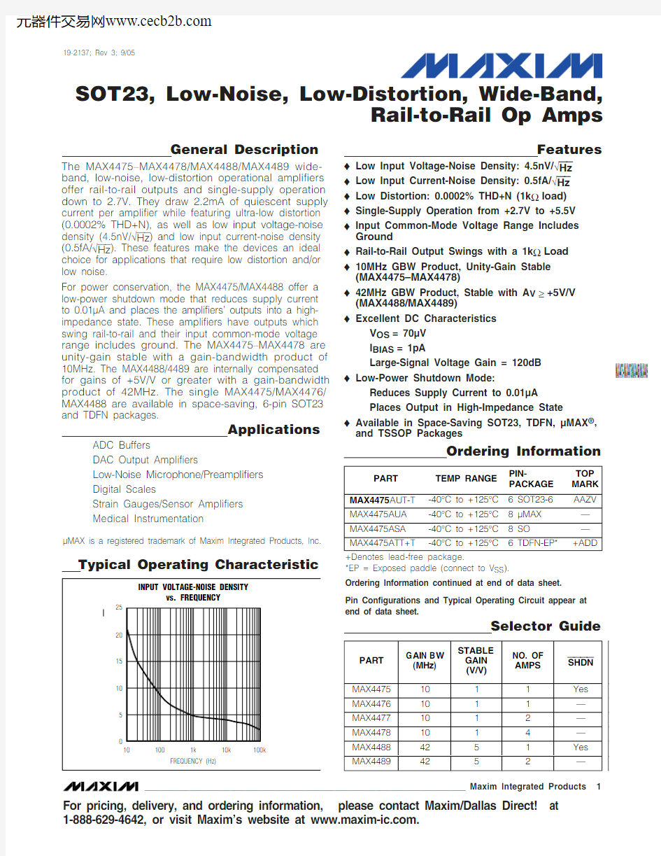
The MAX4475–MAX4478/MAX4488/MAX4489 wide-band, low-noise, low-distortion operational amplifiers offer rail-to-rail outputs and single-supply operation down to 2.7V. They draw 2.2mA of quiescent supply current per amplifier while featuring ultra-low distortion (0.0002% THD+N), as well as low input voltage-noise density (4.5nV/√Hz ) and low input current-noise density (0.5fA/√Hz ). These features make the devices an ideal choice for applications that require low distortion and/or low noise.
For power conservation, the MAX4475/MAX4488 offer a low-power shutdown mode that reduces supply current to 0.01μA and places the amplifiers’ outputs into a high-impedance state. These amplifiers have outputs which swing rail-to-rail and their input common-mode voltage range includes ground. The MAX4475–MAX4478 are unity-gain stable with a gain-bandwidth product of 10MHz. The MAX4488/4489 are internally compensated for gains of +5V/V or greater with a gain-bandwidth product of 42MHz. The single MAX4475/MAX4476/MAX4488 are available in space-saving, 6-pin SOT23and TDFN packages.
Applications
ADC Buffers
DAC Output Amplifiers
Low-Noise Microphone/Preamplifiers Digital Scales
Strain Gauges/Sensor Amplifiers Medical Instrumentation
Features
?Low Input Voltage-Noise Density: 4.5nV/√Hz ?Low Input Current-Noise Density: 0.5fA/√Hz ?Low Distortion: 0.0002% THD+N (1k ?load)?Single-Supply Operation from +2.7V to +5.5V ?Input Common-Mode Voltage Range Includes Ground
?Rail-to-Rail Output Swings with a 1k ?Load ?10MHz GBW Product, Unity-Gain Stable (MAX4475–MAX4478)
?42MHz GBW Product, Stable with A V ≥+5V/V (MAX4488/MAX4489)
?
Excellent DC Characteristics V OS = 70μV I BIAS = 1pA
Large-Signal Voltage Gain = 120dB ?
Low-Power Shutdown Mode:
Reduces Supply Current to 0.01μA Places Output in High-Impedance State
?
Available in Space-Saving SOT23, TDFN, μMAX ?,and TSSOP Packages
MAX4475–MAX4478/MAX4488/MAX4489
SOT23, Low-Noise, Low-Distortion, Wide-Band,
Rail-to-Rail Op Amps
Selector Guide
19-2137; Rev 3; 9/05
For pricing, delivery, and ordering information,please contact Maxim/Dallas Direct!at 1-888-629-4642, or visit Maxim’s website at https://www.360docs.net/doc/601710992.html,.
Ordering Information continued at end of data sheet.*EP = Exposed paddle (connect to V SS ).
Pin Configurations and Typical Operating Circuit appear at end of data sheet.
25
20
10
5
010
1k 10k
100
100k
INPUT VOLTAGE-NOISE DENSITY
vs. FREQUENCY
M A X 4475 t o c 20
FREQUENCY (Hz)
15
V I N E Q U I V A L E N T I N P U T N O I S E V O L T A G E (n V /√H z )
Typical Operating Characteristic
μMAX is a registered trademark of Maxim Integrated Products, Inc.
M A X 4475–M A X 4478/M A X 4488/M A X 4489
Rail-to-Rail Op Amps 2_______________________________________________________________________________________
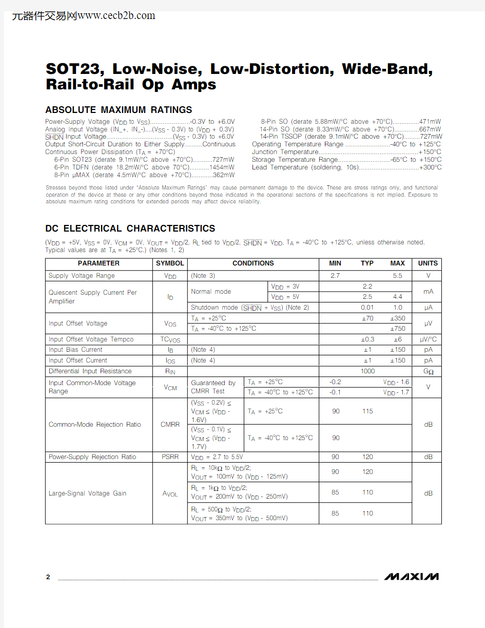
ABSOLUTE MAXIMUM RATINGS
DC ELECTRICAL CHARACTERISTICS
(V DD = +5V, V SS = 0V, V CM = 0V, V OUT = V DD /2, R L tied to V DD /2, SHDN = V DD , T A = -40°C to +125°C, unless otherwise noted.Typical values are at T
= +25°C.) (Notes 1, 2)
Stresses beyond those listed under “Absolute Maximum Ratings” may cause permanent damage to the device. These are stress ratings only, and functional operation of the device at these or any other conditions beyond those indicated in the operational sections of the specifications is not implied. Exposure to absolute maximum rating conditions for extended periods may affect device reliability.
Power-Supply Voltage (V DD to V SS )......................-0.3V to +6.0V Analog Input Voltage (IN_+, IN_-)....(V SS - 0.3V) to (V DD + 0.3V)SHDN Input Voltage....................................(V SS - 0.3V) to +6.0V Output Short-Circuit Duration to Either Supply..........Continuous Continuous Power Dissipation (T A = +70°C)
6-Pin SOT23 (derate 9.1mW/°C above +70°C)...........727mW 6-Pin TDFN (derate 18.2mW/°C above 70°C)...........1454mW 8-Pin μMAX (derate 4.5mW/°C above +70°C)............362mW
8-Pin SO (derate 5.88mW/°C above +70°C)...............471mW 14-Pin SO (derate 8.33mW/°C above +70°C)..............667mW 14-Pin TSSOP (derate 9.1mW/°C above +70°C).........727mW Operating Temperature Range .........................-40°C to +125°C Junction Temperature......................................................+150°C Storage Temperature Range.............................-65°C to +150°C Lead Temperature (soldering, 10s).................................+300°C
MAX4475–MAX4478/MAX4488/MAX4489
Rail-to-Rail Op Amps
DC ELECTRICAL CHARACTERISTICS (continued)
(V DD = +5V, V SS = 0V, V CM = 0V, V OUT = V DD /2, R L tied to V DD /2, SHDN = V DD , T A = -40°C to +125°C, unless otherwise noted.
42108612141618-50-30-20-40-1001020304050
INPUT OFFSET VOLTAGE DISTRIBUTION
V OS (μV)
P E R C E N T A G E O F U N I T S (%
)
-250
-100-150-2000-5020015010050250-50
-250255075100125OFFSET VOLTAGE vs. TEMPERATURE
TEMPERATURE (°C)I N P U T O F F S E T V O L T A G E (μV )
1030
20
40
50
-0.5 1.50.5 2.5 3.5 4.5
INPUT OFFSET VOLTAGE
vs. INPUT COMMON-MODE VOLTAGE
INPUT COMMON-MODE VOLTAGE (V)
I N P U T O F F S E T V O L T A G E (μV )
Typical Operating Characteristics
(V DD = +5V, V SS = 0V, V CM = 0V, V OUT = V DD /2, R L tied to V DD /2, input noise floor of test equipment =10nV/√Hz for all distortion measurements, T A = +25°C, unless otherwise noted.)
M A X 4475–M A X 4478/M A X 4488/M A X 4489
Rail-to-Rail Op Amps 4_______________________________________________________________________________________
Note 1:All devices are 100% tested at T A = +25°C. Limits over temperature are guaranteed by design.Note 2:SHDN is available on the MAX4475/MAX4488 only.Note 3:Guaranteed by the PSRR test.Note 4:Guaranteed by design.
Note 5:
Full-power bandwidth for unity-gain stable devices (MAX4475–MAX4478) is measured in a closed-loop gain of +2V/V to accommodate the input voltage range, V OUT = 4V P-P .
Note 6:Lowpass-filter bandwidth is 22kHz for f = 1kHz and 80kHz for f = 20kHz. Noise floor of test equipment = 10nV/√Hz .
AC ELECTRICAL CHARACTERISTICS (continued)
(V = +5V, V = 0V, V = 0V, V = V /2, R tied to V /2, SHDN = V , T = +25°C.)
Typical Operating Characteristics (continued)
(V DD = +5V, V SS = 0V, V CM = 0V, V OUT = V DD /2, R L tied to V DD /2, input noise floor of test equipment =10nV/√Hz for all distortion measurements, T A = +25°C, unless otherwise noted.)
MAX4475–MAX4478/MAX4488/MAX4489
Rail-to-Rail Op Amps
_______________________________________________________________________________________5
00.05
0.10
0.15
0.200.25
4
5
2
3
1
6
7
8
9
10
OUTPUT VOLTAGE vs. OUTPUT LOAD CURRENT
OUTPUT LOAD CURRENT (mA)
O U T P U T V O L T A G E (V )
2010
40306050
70-50
25
-25
50
75
100
125
OUTPUT VOLTAGE SWING (V OH )
vs. TEMPERATURE
TEMPERATURE (°C)
V D D - V O H (m V )
020
104030605070
-50
25
-25
50
75
100
125
OUTPUT VOLTAGE SWING (V OL )
vs. TEMPERATURE
TEMPERATURE (°C)
V O L (m V )
50
607080901001101201300
50
100
150
200
250LARGE-SIGNAL VOLTAGE GAIN vs. OUTPUT VOLTAGE SWING
V OUT SWING FROM EITHER SUPPLY (mV)A V (d B )
50
607080901001101201300
50
100
150
200
250
LARGE-SIGNAL VOLTAGE GAIN vs. OUTPUT VOLTAGE SWING
V OUT SWING FROM EITHER SUPPLY (mV)A V (d B )
50
60708090100110120130
50
100
150
200
250
LARGE-SIGNAL VOLTAGE GAIN vs. OUTPUT VOLTAGE SWING
V OUT SWING FROM EITHER SUPPLY (mV)
A V (d
B )
50
607080901001101201300
50
100
150
200
250
LARGE-SIGNAL VOLTAGE GAIN vs. OUTPUT VOLTAGE SWING
V OUT SWING FROM EITHER SUPPLY (mV)A V (d B )
50
70601009080
130120110140-50
25
-25
50
75
100
125
LARGE-SIGNAL VOLTAGE GAIN
vs. TEMPERATURE
TEMPERATURE (°C)
A V O L (d
B )
1.00.5
2.01.52.5
3.0
-50
25
50
-25
75
100
125
SUPPLY CURRENT vs. TEMPERATURE
TEMPERATURE (°C)
S U P P L Y C U R R E N T (m A )
M A X 4475–M A X 4478/M A X 4488/M A X 4489
Rail-to-Rail Op Amps 6_______________________________________________________________________________________
Typical Operating Characteristics (continued)
(V DD = +5V, V SS = 0V, V CM = 0V, V OUT = V DD /2, R L tied to V DD /2, input noise floor of test equipment =10nV/√Hz for all distortion measurements, T A = +25°C, unless otherwise noted.)
01.00.52.01.52.53.0
2.5
3.5
4.0
3.0
4.5
5.0
5.5SUPPLY CURRENT vs. SUPPLY VOLTAGE
SUPPLY VOLTAGE (V)S U P P L Y C U R R E N T (m A )
1.00.5
2.01.52.5
3.0021345
SUPPLY CURRENT vs. OUTPUT VOLTAGE
M A X 4475 t o c 14
OUTPUT VOLTAGE (V)
S U P P L Y C U R R E N T (m A )
V DD = 5V
V DD = 3V
-20
-15
-10-505101520
2.5
3.5
3.0
4.0
4.5
5.0
5.5
INPUT OFFSET VOLTAGE vs. SUPPLY VOLTAGE
M A X 4475 t o c 15
SUPPLY VOLTAGE (V)
I N P U T O F F S E T V O L T A G E (μV )
MAX4475–MAX4478
GAIN AND PHASE vs. FREQUENCY
INPUT FREQUENCY (Hz)
100
100k
1M
10M
1k
10k
100M
G A I N (d B )
60-40
-30-20-1001020504030
P H A S E (d e g r e e s )180-144
-108-72-36036
14410872
MAX4488/MAX4489
GAIN AND PHASE vs. FREQUENCY
INPUT FREQUENCY (Hz)
100
100k 1M 10M
1k
10k 100M
G A I N (d B )
60-40
-30-20-1001020
504030-180P H A S E (d e g r e e s )
180-144
-108-72
-36036144108721000100,000
-130
-10-20
-30-40-50-60-70-80-90-100-110-1200
0.0010.1
10MAX4475–MAX4478
POWER-SUPPLY REJECTION RATIO
vs. FREQUENCY
FREQUENCY (kHz)
P S R R (d B )
1000
100
10
1
0.10.01
11001k 1010k
OUTPUT IMPEDANCE vs. FREQUENCY
FREQUENCY (Hz)
O U T P U T I M P E D A N C E (?)
MAX4475–MAX4478/MAX4488/MAX4489
Rail-to-Rail Op Amps
_______________________________________________________________________________________7
25
2010
5
10
1k 10k
100
100k
INPUT VOLTAGE-NOISE DENSITY
vs. FREQUENCY
M A X 4475 t o c 20
FREQUENCY (Hz)
15
V I N E Q U I V A L E N T I N P U T N O I S E V O L T A G E (n V /H z )
1s/div
0.1Hz TO 10Hz P-P NOISE
V DD = 3V OR 5V
V P-P NOISE = 260nV P-P
MAX4475
TOTAL HARMONIC DISTORTION PLUS NOISE
OUTPUT VOLTAGE (V P-P )
T H D + N (%)
10
0.0001
0.001
0.01
0.1
10
2
1
3
4
MAX4488/MAX4489
TOTAL HARMONIC DISTORTION PLUS NOISE
OUTPUT VOLTAGE (V P-P )
2
1
3
T H D + N (%)
10
0.00001
0.00010.0010.0110.1
0.01
0.0001
10k 20k
MAX4488/MAX4489
TOTAL HARMONIC DISTORTION FREQUENCY (Hz)
T H D + N (%)
0.001
5k
15k
0.01
0.001
20k
MAX4475–MAX4478
TOTAL HARMONIC DISTORTION PLUS NOISE
FREQUENCY (Hz)
T H D + N (%)
5k
10k
15k 1
0.0001
5k
15k
20k
MAX4488/MAX4489
TOTAL HARMONIC DISTORTION PLUS NOISE
0.001
0.010.1FREQUENCY (Hz)
T H D + N (%)
10k Typical Operating Characteristics (continued)
(V DD = +5V, V SS = 0V, V CM = 0V, V OUT = V DD /2, R L tied to V DD /2, input noise floor of test equipment =10nV/√Hz for all distortion measurements, T A = +25°C, unless otherwise noted.)
1μs/div
MAX4475–MAX4478
LARGE-SIGNAL PULSE RESPONSE
V DD = 3V, R L = 10k ?, C L = 100pF V IN = 2V
0.5V MAX4475 toc27
2.5V
4μs/div
MAX4475–MAX4478
SMALL-SIGNAL PULSE RESPONSE
V DD = 3V, R L = 10k ?, C L = 100pF V IN = 100mV PULSE
0.5V
MAX4475 toc28
0.6V
20mV/div
M A X 4475–M A X 4478/M A X 4488/M A X 4489
Rail-to-Rail Op Amps Typical Operating Characteristics (continued)
(V DD = +5V, V SS = 0V, V CM = 0V, V OUT = V DD /2, R L tied to V DD /2, input noise floor of test equipment =10nV/√Hz for all distortion measurements, T A = +25°C, unless otherwise noted.)
1μs/div
MAX4488/MAX4489
LARGE-SIGNAL PULSE RESPONSE
V DD = 3V, R L = 10k ?, C L = 50pF V IN = 20mV PULSE, A V = +5V/V
MAX4475 toc29V OUT
200mV/div
1μs/div
MAX4488/MAX4489
SMALL-SIGNAL PULSE RESPONSE
V DD = 3V, R L = 10k ?, C L = 50pF V IN = 20mV PULSE, A V = +5V/V
MAX4475 toc30
V OUT 50mV/div
1.6V 1.5V
-20-90
10
1000
100
100k
100M
10M MAX4477/MAX4478/MAX4489CROSSTALK vs. FREQUENCY
-60-50-40-30M A X 4475 t o c 31
FREQUENCY (Hz)
C R O S S T A L K (d B )
10k 1M
-70-80
Detailed Description
The MAX4475–MAX4478/MAX4488/MAX4489 single-supply operational amplifiers feature ultra-low noise and distortion. Their low distortion and low noise make them ideal for use as preamplifiers in wide dynamic-range applications, such as 16-bit analog-to-digital converters (see Typical Operating Circuit ). Their high-input impedance and low noise are also useful for sig-nal conditioning of high-impedance sources, such as piezoelectric transducers.
These devices have true rail-to-rail ouput operation,drive loads as low as 1k ?while maintining DC accura-cy, and can drive capactive loads up to 200pF without oscillation. The input common-mode voltage range extends from (V DD - 1.6V) to 200mV below the negative rail. The push-pull output stage maintains excellent DC characteristics, while delivering up to ±5mA of current.The MAX4475–MAX4478 are unity-gain stable, while the MAX4488/MAX4489 have a higher slew rate and are stable for gains ≥5V/V. The MAX4475/MAX4488feature a low-power shutdown mode, which reduces the supply current to 0.01μA and disables the outputs.
Low Distortion
Many factors can affect the noise and distortion that the device contributes to the input signal. The following guidelines offer valuable information on the impact of design choices on Total Harmonic Distortion (THD).Choosing proper feedback and gain resistor values for a particular application can be a very important factor in reducing THD. In general, the smaller the closed-loop gain, the smaller the THD generated, especially when driving heavy resistive loads. The THD of the part normally increases at approximately 20dB per decade,as a function of frequency. Operating the device near or above the full-power bandwidth significantly degrades distortion.
Referencing the load to either supply also improves the part’s distortion performance, because only one of the MOSFETs of the push-pull output stage drives the out-put. Referencing the load to midsupply increases the part’s distortion for a given load and feedback setting.(See the Total Harmonic Distortion vs. Frequency graph in the Typical Operating Characteristics .)
For gains ≥5V/V, the decompensated devices MAX4488/MAX4489 deliver the best distortion perfor-mance, since they have a higher slew rate and provide a higher amount of loop gain for a given closed-loop gain setting. Capacitive loads below 100pF do not sig-nificantly affect distortion results. Distortion perfor-mance is relatively constant over supply voltages.
MAX4475–MAX4478/MAX4488/MAX4489
Rail-to-Rail Op Amps
_______________________________________________________________________________________9
V 100mV/div
V 100mV/div
A V = +2
R F = R G = 100k ?
2μs/div
Figure 1. Adding Feed-Forward Compensation
Figure 2a. Pulse Response with No Feed-Forward Compensation
V OUT
100mV/div
V IN
100mV/div
A V = +2
R F = R G = 100k ?
2μs/div
M A X 4475–M A X 4478/M A X 4488/M A X 4489
Rail-to-Rail Op Amps 10______________________________________________________________________________________
Low Noise
The amplifier’s input-referred noise-voltage density is dominated by flicker noise at lower frequencies, and by thermal noise at higher frequencies. Because the ther-mal noise contribution is affected by the parallel combi-nation of the feedback resistive network (R F || R G ,Figure 1), these resistors should be reduced in cases where the system bandwidth is large and thermal noise is dominant. This noise contribution factor decreases,however, with increasing gain settings.
For example, the input noise-voltage density of the cir-cuit with R F = 100k ?, R G = 11k ?(A V = +5V/V) is e n = 14nV/√Hz , e n can be reduced to 6nV/√Hz by choosing R F = 10k ?, R G = 1.1k ?(A V = +5V/V), at the expense of greater current consumption and potentially higher distortion. For a gain of 100V/V with R F = 100k ?,R G = 1.1k ?, the e n is still a low 6nV/√Hz .
Using a Feed-Forward Compensation
Capacitor, C Z
The amplifier’s input capacitance is 10pF. If the resis-tance seen by the inverting input is large (feedback network), this can introduce a pole within the amplifier’s bandwidth resulting in reduced phase https://www.360docs.net/doc/601710992.html,pensate the reduced phase margin by introducing a feed-forward capacitor (C Z ) between the inverting input and the output (Figure 1). This effectively cancels the pole from the inverting input of the amplifier.Choose the value of C Z as follows:
C Z = 10 x (R F / R G ) [pF]
In the unity-gain stable MAX4475–MAX4478, the use of a proper C Z is most important for A V = +2V/V, and A V = -1V/V. In the decompensated MAX4488/MAX4489, C Z is most important for A V = +10V/V.Figures 2a and 2b show transient response both with and without C Z .
Using a slightly smaller C Z than suggested by the for-mula above achieves a higher bandwidth at the expense of reduced phase and gain margin. As a gen-eral guideline, consider using C Z for cases where R G ||R F is greater than 20k ?(MAX4475–MAX4478) or greater than 5k ?(MAX4488/MAX4489).
Applications Information
The MAX4475–MAX4478/MAX4488/MAX4489 combine good driving capability with ground-sensing input and rail-to-rail output operation. With their low distortion and low noise, they are ideal for use in ADC buffers, med-ical instrumentation systems and other noise-sensitive applications.
Ground-Sensing and Rail-to-Rail Outputs
The common-mode input range of these devices extends below ground, and offers excellent common-mode rejection. These devices are guaranteed not to undergo phase reversal when the input is overdriven (Figure 3).
Figure 4 showcases the true rail-to-rail output operation of the amplifier, configured with A V = 5V/V. The output swings to within 8mV of the supplies with a 10k ?load,making the devices ideal in low-supply voltage applica-tions.
Power Supplies and Layout
The MAX4475–MAX4478/MAX4488/MAX4489 operate from a single +2.7V to +5.5V power supply or from dual supplies of ±1.35V to ±2.75V. For single-supply opera-tion, bypass the power supply with a 0.1μF ceramic
V OUT 2V/div
V IN 2V/div
0V
A V = +1V DD = +5V R L = 10k ?
40μs/div
V 1V/div
20μs/div
Figure 3. Overdriven Input Showing No Phase Reversal
Figure 4. Rail-to-Rail Output Operation
MAX4475–MAX4478/MAX4488/MAX4489
Rail-to-Rail Op Amps
______________________________________________________________________________________11
capacitor placed close to the V DD pin. If operating from dual supplies, bypass each supply to ground.
Good layout improves performance by decreasing the amount of stray capacitance and noise at the op amp’s inputs and output. To decrease stray capacitance, min-imize PC board trace lengths and resistor leads, and place external components close to the op amp’s pins.
Typical Application Circuit
The Typical Application Circuit shows the single MAX4475 configured as an output buffer for the MAX5541 16-bit DAC. Because the MAX5541 has an unbuffered voltage output, the input bias current of the op amp used must be less than 6nA to maintain 16-bit accuracy. The MAX4475 has an input bias current of only 150pA (max), virtually eliminating this as a source
of error. In addition, the MAX4475 has excellent open-loop gain and common-mode rejection, making this an excellent ouput buffer amplifier.
DC-Accurate Lowpass Filter
The MAX4475–MAX4478/MAX4488/MAX4489 offer a unique combination of low noise, wide bandwidth, and high gain, making them an excellent choice for active filters up to 1MHz. The Typical Operating Circuit shows the dual MAX4477 configured as a 5th order Chebyschev filter with a cutoff frequency of 100kHz.The circuit is implemented in the Sallen-Key topology,
making this a DC-accurate filter.
Pin Configurations
M A X 4475–M A X 4478/M A X 4488/M A X 4489
12______________________________________________________________________________________
Rail-to-Rail Op Amps
Ordering Information (continued)Chip Information
MAX4475–MAX4478/MAX4488/MAX4489Rail-to-Rail Op Amps
MAX4475/MAX4476 TRANSISTOR COUNT: 1095 Array MAX4477 TRANSISTOR COUNT: 2132
MAX4478 TRANSISTOR COUNT: 4244
MAX4488 TRANSISTOR COUNT: 1095
MAX4489 TRANSISTOR COUNT: 2132
PROCESS: BiCMOS
+Denotes lead-free package.
*EP = Exposed paddle (connect to V SS).
______________________________________________________________________________________13
M A X 4475–M A X 4478/M A X 4488/M A X 4489
Rail-to-Rail Op Amps 14______________________________________________________________________________________
Package Information
(The package drawing(s) in this data sheet may not reflect the most current specifications. For the latest package outline information,go to https://www.360docs.net/doc/601710992.html,/packages .)
MAX4475–MAX4478/MAX4488/MAX4489
Rail-to-Rail Op Amps
15
Package Information (continued)
(The package drawing(s) in this data sheet may not reflect the most current specifications. For the latest package outline information,go to https://www.360docs.net/doc/601710992.html,/packages .)
M A X 4475–M A X 4478/M A X 4488/M A X 4489
Rail-to-Rail Op Amps 16______________________________________________________________________________________
Package Information (continued)
(The package drawing(s) in this data sheet may not reflect the most current specifications. For the latest package outline information,go to https://www.360docs.net/doc/601710992.html,/packages .)
MAX4475–MAX4478/MAX4488/MAX4489
Rail-to-Rail Op Amps
Maxim cannot assume responsibility for use of any circuitry other than circuitry entirely embodied in a Maxim product. No circuit patent licenses are implied. Maxim reserves the right to change the circuitry and specifications without notice at any time.
Maxim Integrated Products, 120 San Gabriel Drive, Sunnyvale, CA 94086 408-737-7600 ____________________17?2005 Maxim Integrated Products
Printed USA
is a registered trademark of Maxim Integrated Products, Inc.
Package Information (continued)
(The package drawing(s) in this data sheet may not reflect the most current specifications. For the latest package outline information,go to https://www.360docs.net/doc/601710992.html,/packages .)