11-SILICON-LIGHT A EUROPEAN FP7 PROJECT AIMING AT HIGH EFFICIENCY THIN FILM SILICON

SILICON-LIGHT: A EUROPEAN FP7 PROJECT AIMING AT HIGH EFFICIENCY THIN FILM SILICON
SOLAR CELLS ON FOIL
W. Soppe*1, F-J Haug2, P. Couty3, M. Duchamp4, W. Schipper5, J. Krc6, G. Sanchez7, K. Leitner8, Q. Wang9.
*Corresponding author, phone +31 (224) 56 4761, e-mail: soppe@ecn.nl
1 ECN Solar Energy, P.O. Box 1, 1755 ZG Petten, The Netherlands;
2 Ecole Polytechnique Federale de Lausanne (EPFL),
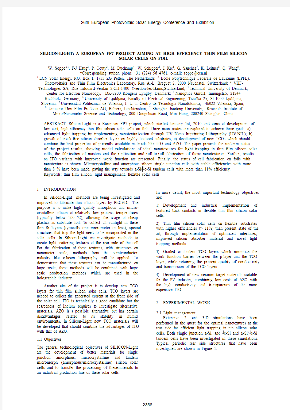
Photovoltaics and Thin Film Electronics Laboratory, Rue A.-L. Breguet 2, 2000 Neuchatel, Switzerland; 3 VHF-Technologies SA, Rue Edouard-Verdan 2,CH-1400 Yverdon-les-Bains,Switzerland; 4 Technical University of Denmark, Center for Electron Nanoscopy, DK-2800 Kongens Lyngby, Denmark; 5 Nanoptics GmbH, Innungstr.5, 21244 Buchholz, Germany; 6 University of Ljubljana, Faculty of Electrical Engineering, Tr?a?ka 25, SI-1000 Ljubljana, Slovenia. 7 Universidad Politécnica de Valencia, I. U. I. Centro de Tecnología Nanofotónica, 46022 Valencia, Spain;
8 Umicore Thin Film Products AG, Balzers, Liechtenstein; 9 Shanghai Jiaotong University, Research Institute of
Micro/Nanometer Science and Technology, 800 Dongchuan Road, Min Hang, 200240 Shanghai, China.
ABSTRACT: Silicon-Light is a European FP7 project, which started January 1st, 2010 and aims at development of low cost, high-efficiency thin film silicon solar cells on foil. Three main routes are explored to achieve these goals: a) advanced light trapping by implementing nanotexturization through UV Nano Imprinting Lithography (UV-NIL); b) growth of crack-free silicon absorber layers on highly textured substrates; c) development of new TCOs which should combine the best properties of presently available materials like ITO and AZO. The paper presents the midterm status of the project results, showing model calculations of ideal nanotextures for light trapping in thin film silicon solar cells; the fabrication of masters and the replication and roll-to-roll fabrication of these nanotextures. Further, results on ITO variants with improved work function are presented. Finally, the status of cell fabrication on foils with nanotexture is shown. Microcrystalline and amorphous silicon single junction cells with stable efficiencies with more than 8 % have been made, paving the way towards a-Si/c-Si tandem cells with more than 11% efficiency.
Keywords: thin film silicon, light management, flexible solar cells
1 INTRODUCTION
In Silicon-Light methods are being investigated and improved to fabricate thin silicon layers by PECVD. The purpose is to make high quality amorphous and micro-crystalline silicon at relatively low process temperatures (typically below 200 oC), allowing the usage of cheap plastics as substrate foil. To collect all sunlight in these thin Si layers (typically one micrometer or less), special structures that trap the light need to be incorporated in the solar cells. In Silicon-Light we investigate methods to create light-scattering textures at the rear side of the cell. For the fabrication of these textures, with structures on nanometer scale, methods from the semiconductor industry like e-beam lithography will be applied. To demonstrate that these textures can be manufactured on large scale, these methods will be combined with large scale production methods which are used in the holographic industry.
Another aim of the project is to develop new TCO layers for thin film silicon solar cells. TCO layers are needed to collect the generated current at the front side of the solar cell. ITO is technically a good candidate but the scarceness of Indium requires to investigate alternative materials. AZO is a possible alternative but has certain disadvantages related to its stability in humid environments. In Silicon-Light new TCO materials will be developed that should combine the advantages of ITO with that of AZO.
1.1 Objectives
The general technological objectives of SILICON-Light are the development of better materials for single junction amorphous, microcrystalline and tandem micromorph (amorphous/microcrystalline) silicon solar cells and to transfer the processing of these materials to an industrial production line of these solar cells. In more detail, the most important technology objectives are:
1) Development and industrial implementation of textured back contacts in flexible thin film silicon solar cells,
2) Thin film silicon solar cells on flexible substrates with higher efficiencies (> 11%) than present state of the art, through implementation of optimized interfaces, improved silicon absorber material and novel light trapping methods.
3) Graded or tandem TCO layers which minimize the work function barrier between the p-layer and the TCO layer, while retaining the present quality of conductivity and transmission of the TCO layers.
4) Development of new ceramic target materials suitable for the PV industry, combining low costs of AZO with the high conductivity and transparency of the more expensive ITO.
2 EXPERIMENTAL WORK
2.1 Light management
Extensive 2- and 3-D simulations have been performed in the quest for the optimal nanotextures at the rear side for efficient light trapping in nip silicon solar cells. Both single junction a-Si, and c-Si and a-Si/c-Si tandem cells have been investigated in these simulations. Typical periodic rear side structures that have been investigated are shown in Figure 1.
Figure 1: Examples of analysed periodic textures: (a) rectangular, (b) triangular, (c) sinusoidal, and (d) U-like. The period (P) and height (h) parameters are also indicated.
The simulations show that periodic textures which are introduced by the substrate at the rear side and are transferred through conformal growth to the subsequent layers can increase the generated current in the solar cells (a-Si and c-Si) with at least 30% if the right period/height combinations are chosen [1]. It seems that light trapping capabilities of triangular, rectangular and sinusoidal structures are quite similar. In practice, however, conformal and defect-free growth of silicon layers on these structures is not straightforward and therefore is also subject of research in Silicon-Light.
2.2 Growth of nip Si solar cells on periodically textured
substrates
One of the tasks in the project is to explore the limits of conformal growth of layers on textured substrates. For this purpose silicon masters were made with extreme high aspect ratios, by e-beam lithography. These masters (or Ni replicas) were used to imprint a UV-hardening lacquer that was applied on the substrate, consisting of steel or plastic foil. After UV-hardening, a Ag/ZnO back reflector was sputtered, followed by c-Si nip deposition by PECVD and a sputtered ITO layer. In Fig. 2 an example of a nip stack on a texture with an extreme aspect ratio is shown. This texture consists of rectangular pillars with width of about 250 nm, and a height and period of about 750 nm.
It is clear that, for this extreme texture, the growth of the cell stack is far from conformal. This already starts with the Ag/ZnO layers (light-gray) and becomes worse for the c-Si layers (dark gray), which build up large voids at the periodic boundaries.
For application in solar cells, more rounded textures, like sinusoidal structures, are required but the fabrication of such structures by e-beam lithography is quite a challenge. Nonetheless, we have been able to fabricate first examples of such structures, as to be seen in Fig 3.
Figure 3: examples of rounded textures made by combination of reactive ion etching, e-beam lithography and plasma assisted deposition.
2.3 TCO development
In Silicon-Light we focus on sputtering as deposition technology for TCOs. The work TCO in the project has two major topics: 1) development of new TCOs which should combine the best properties of e.g. ITO and AZO. This is an elaborate process and first results are expected to arrive in the second half of the project. 2) Enhancing the V oc of a-Si (top) cells by increasing the work function of the top TCO. Commonly used TCOs like ITO, FTO or AZO are n-type semiconductors, creating a p-n junction at the interface with the p-layer. Because of the much higher carrier density in TCO, the band bending is restricted entirely to the p-layer, making this interface effectively a Schottky type junction. A high work function of the TCO should reduce the potential losses associated with this Schottky barrier.
We have investigated the work function of ITO films with different compositions deposited by DC sputtering. The work function has been determined by an ex-situ Kelvin probe under nitrogen atmosphere. Figure 3 shows that the addition of oxygen can increase the work function significantly. Among the different compositions it appears that the work function depends also on the In/Sn ratio in the target: lower Sn content generally yields higher values. Further details and a discussion of electrical and optical properties of the films with different In 2O 3-Sn02 compositions can be found in [2].
Figure 2: cross sectional SEM image of an c-Si nip
cell on a texture with extreme aspect ratio. ITO nip Si Ag/ZnO lacquer- pillars
Figure 4: The work function of ITO as a function of addition of oxygen to the sputtering process; for targets of various In/Sn ratios.
We incorporated the ITO films onto amorphous n-i-p solar cells. Figure 5 shows and example of the 90/10 composition for the case of flat and textured cells. We attribute the gain in V oc with oxygen partial pressure to the corresponding increase in work function shown in Figure4.
Figure 5: V oc of a-Si nip cells with ITO sputtered under various oxygen partial pressures. The figure shows results of cells made on both textured and flat substrates.
2.4 Cell results
Besides the investigation of TCOs with higher work functions, we also explored the usage of p-nc-SiOx window layer. Both should contribute to higher V oc of a-Si cells, with the additional effect of increasing the total V oc of a-Si/c-Si tandem cells. In Figure 6 we show cell parameters obtained for various compositions of these window layers. Maximum values of 935 mV have been achieved for a-Si nip solar cells [3].
Figure 6: Cell parameters of a-Si cells with p-SiOx window layers with various oxygen condentrations.
Cells with the p-type SiO x layer were incorporated into micromorph tandem cells. Figure 7 shows that the the EQE of the top cell benefits from the high transparency of this high bandgap window layer. The cells with two different types of back reflector exceed initial efficiencies of 10%.
Figure 7: External quantum efficiencies of tandem cells on two different substrates, with relatively thin absorbers of 1.3 μm and 200 nm for the microcrystalline bottom and the amorphous top cell, respectively.
2.5 Upscaling and industrial implementation
Implementation of lab-scale solutions in industrial (pilot) lines is one of the most important goals of the project. For the application of periodic texturization, we develop methods derived from the holographic industry to achieve this goal. Small Si masters (typically 5×5 mm 2) are replicated and stitched to create large shims which can be used for roll-to-roll nano-imprinting in UV
W o r k f u n c t i o n (e V )
Oxygen partial pressure (%)
Oxygen partial pressure
O p e n c i r c u i t v o l t a g e [V
]
E Q E
Wavelength (nm)
hardening lacquer on foil on industrial scale. In Figure 7
an example of such texturization on steel foil is shown.
3 DISCUSSION AND OUTLOOK
The project Silicon-Light is running now for more than one year and many important targets are still to be achieved. We made, however, important progress in determining and fabricating ideal rear side textures for nip a-Si and c-Si solar cells on foil and we have developed technologies to upscale this texturization method for mass production. The next step will be to fabricate shims with the ideal periodic structures for a-Si and c-Si cells and to implement these textures in industrial production of thin film silicon solar cells.
In the second half of the project we will also harvest climate chamber test results of new TCO layers that have been developed in the project. These results should point us towards (sputtered) TCO materials which combine the low material costs of AZO with the good electronic properties and climate stability of ITO.
The present status of cell efficiencies in the consortium is that for small areas a-Si/c-Si nip cells on foil with efficiencies of almost 10 % have been made. These cell efficiencies have been reached using random textures for light trapping. Through application of optimized periodic textures and improved a-Si top cells with increased Voc, we should be able to reach one of the final targets of the project: thin film silicon solar cells on foil with stabilized efficiencies of more than 11%. ACKNOWLEDGEMENTS
This work was funded by the European FP7 project Silicon-Light (GA No. 241277)
REFERENCES
[1] B. Lipov?ek, M. Cvek, A. ?ampa, J. Kr?, M. Topi?,
Presented at the 25th European Photovoltaic Solar
Energy Conference and Exhibition, 6-10 September 2010, Valencia, Spain
[2] Franz-Jozef Haug et al, “Improvement of the open
circuit voltage by modifying the work-function of the transparent front electrode in amorphous n-i-p solar cells”, submitted to Progress in Photovoltaics [3] R.Biron, C. Pahud, F.-J. Haug, J. Escarré, K.
S?derstr?m, C. Ballif, Window layer with p doped silicon oxide for high V oc thin-film silicon n-i-p solar cells, submitted to Journal of Applied Physics
Figure 8: Periodic texture on steel foil made by roll-to-roll nano-imprinting.