203d6
NCP1203
PWM Current-Mode Controller for Universal Off-Line Supplies Featuring Standby and Short Circuit Protection
Housed in SOIC?8 or PDIP?8 package, the NCP1203 represents a major leap toward ultra?compact Switchmode Power Supplies and represents an excellent candidate to replace the UC384X devices. Due to its proprietary SMARTMOS Very High Voltage Technology, the circuit allows the implementation of complete off?line AC?DC adapters, battery charger and a high?power SMPS with few external components.
With an internal structure operating at a fixed 40 kHz, 60 kHz or 100 kHz switching frequency, the controller features a high?voltage startup FET which ensures a clean and loss?less startup sequence. Its current?mode control naturally provides good audio?susceptibility and inherent pulse?by?pulse control.
When the current setpoint falls below a given value, e.g. the output power demand diminishes, the IC automatically enters the so?called skip cycle mode and provides improved efficiency at light loads while offering excellent performance in standby conditions. Because this occurs at a user adjustable low peak current, no acoustic noise takes place.
The NCP1203 also includes an efficient protective circuitry which, in presence of an output over load condition, disables the output pulses while the device enters a safe burst mode, trying to restart. Once the default has gone, the device auto?recovers. Finally, a temperature shutdown with hysteresis helps building safe and robust power supplies.
Features Pb?Free Packages are Available High?Voltage Startup Current Source Auto?Recovery Internal Output Short?Circuit Protection Extremely Low No?Load Standby Power Current?Mode with Adjustable Skip?Cycle Capability Internal Leading Edge Blanking 250 mA Peak Current Capability Internally Fixed Frequency at 40 kHz, 60 kHz and 100 kHz Direct Optocoupler Connection Undervoltage Lockout at 7.8 V Typical SPICE Models Available for TRANsient and AC Analysis Pin to Pin Compatible with NCP1200
Applications AC?DC Adapters for Notebooks, etc. Offline Battery Chargers Auxiliary Power Supplies (USB, Appliances, TVs, etc.) https://www.360docs.net/doc/6f4259784.html,
MARKING
DIAGRAMS
SOIC?8 8
xxxxxx 8
D1, D2 SUFFIX ALYW
CASE 751 1
1
8
PDIP?8 xxxxxxxxx
N SUFFIX AWL 8
YYWW
CASE 626
1
1
xx = Specific Device Code
A
= Assembly Location WL, L = Wafer Lot Y, YY = Year
W, WW = Work Week
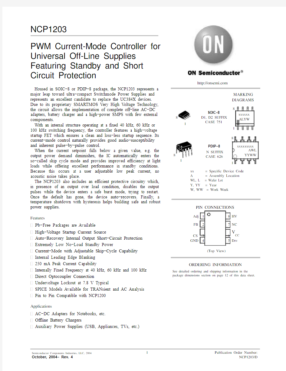
PIN CONNECTIONS
Adj 1 8 HV FB 2 7 NC CS 3 6 V
CC GND 4
5 Drv
(Top View)
ORDERING INFORMATION
See detailed ordering and shipping information in the
package dimensions section on page 12 of this data sheet.
NCP1203
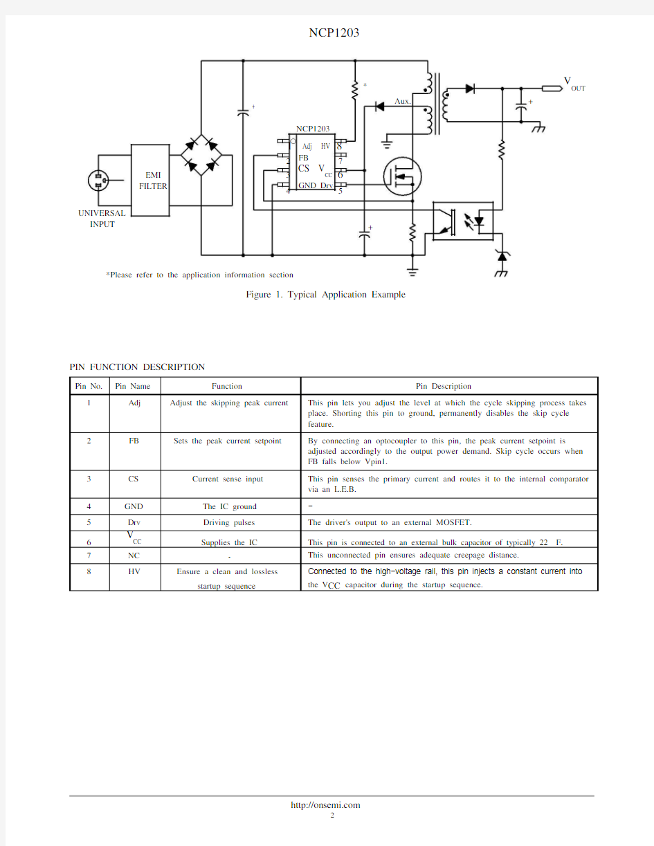
*
V
OUT
+
Aux.
+
NCP1203
1 Adj HV 8
2 FB
7
EMI 3 CS V
CC 6
FILTER
4 GND Drv
5
UNIVERSAL
INPUT
+
*Please refer to the application information section
Figure 1. Typical Application Example
PIN FUNCTION DESCRIPTION
NCP1203
Adj HV 18
HV CURRENT
SOURCE
80 k
1.2 V SKIP CYCLE
NC
FB COMPARATOR
+
UVLO HIGH AND LOW
2-7
INTERNAL V CC INTERNAL REGULATOR
24 k
CURRENT
Q FLIP?FLOP SENSE V CC
250 ns40?60?100 kHz SET DCmax = 80%
Q OVERLOAD
36 L.E.B.CLOCK MANAGEMENT
RESET
20 k57 k+
-
GROUND V
REF
Drv
4 1 V±250 mA5
+25 k
?
Figure 2. Internal Circuit Architecture
MAXIMUM RATINGS
limit values (not normal operating conditions) and are not valid simultaneously. If these limits are exceeded, device functional operation is not implied, damage may occur and reliability may be affected.
NCP1203
ELECTRICAL CHARACTERISTICS (For typical values T J= 25?C, for min/max values T J= 0?C to +125?C, Max T J=
Supply Section (All frequency versions, otherwise noted)
Drive Output
1.Max value at T J = 0?C.
2.Maximum value @ T J = 25?C, please see characterization curves.
3.Pin 5 loaded by 1 nF.
NCP1203
V C C (o n ) T H R E S H O L D (V )
14.0 13.8 13.6 13.4 13.2 13.0 12.8
12.6
12.4 12.2
?25
25 50 75 100 125
TEMPERATURE (?C)
V C C (m i n ) L E V E L (V )
8.4
8.2 8.0 7.8 7.6
7.4
7.2
?25 0 25 50 75 100 125 TEMPERATURE (?C)
Figure 3. V CC(on) Threshold versus
Figure 4. V CC(min) Level versus Temperature
Temperature
( A ) 1000
(m A )
2.0
100 kHz
950
C O N S U M P T I O N 900 C O N S U M P T I O N 1.8
850
800
100 kHz
60 kHz
1.6
750
60 kHz
700 1.4 C U R R E N T 1 n F L O A D
650 40 kHz
600
1.2
, 550
,
40 kHz
C C
C
C
I 500
I 1.0
?25
25
50
75
100
125
?25
25
50
75
100
125
TEMPERATURE (?C) TEMPERATURE (?C)
Figure 5. I C Current Consumption (No Load)
Figure 6. I CC Consumption (Loaded by 1 nF)
versus Temperature versus Temperature
H V C U R R E N T S O U R C E (m A )
( A )
V
6=
C
C
V @ C
C
I
TEMPERATURE (?C)
TEMPERATURE (?C)
Figure 7. HV Current Source at V CC = 10 V
Figure 8. I C Consumption at V CC = 6 V
versus Temperature
versus Temperature