23-Thin Film Silicon Emitters for Crystalline Silicon Solar Cells, epitaxial, amorphous or microcrys
THIN FILM SILICON EMITTERS FOR CRYSTALLINE SILICON SOLAR CELLS,
EPITAXIAL, AMORPHOUS OR MICROCRYSTALLINE ? - A SIMULATION STUDY
R.Stangl*, A.Froitzheim, W.Fuhs
Hahn-Meitner-Institut Berlin, Abt. Silizium Photovoltaik, Kekuléstr. 5, D-12489 Berlin *corresponding author: Dr. Rolf Stangl, Tel: +49/30/67053-312, Fax: ~333, e-mail: stangl@hmi.de ABSTRACT: The performance of solar cells which consist of thin-film silicon emitters of the type epi-Si(n), a-Si(n)/a-Si(i) or μc-Si(n)/a-Si(i) grown on a high quality p-type silicon wafer, is investigated by numerical computer simulation. The influence of the emitter/wafer interface state density, of the front contact surface recombination velocity and of the front contact barrier height on the IV-characteristics of the solar cells is examined. It is shown that applying a TCO as a front contact material, severe degradation of the solar cell performance is to be expected in case of an epi(n) and an a-Si(n)/a-Si(i) emitter due to emitter depletion and reduction of the internal field within the c-Si absorber. It is shown that a μc-Si(n)/a-Si(i) emitter offers some advantages: (1) The cell is almost insensitive to the TCO/emitter contact, and (2) its higher doping efficiency leads to higher short circuit currents and to a better suppression of the emitter/wafer interface recombination.
KEYWORDS: c-Si (1), Si-films (2), heterojunction (3)
1.INTRODUCTION
Silicon solar cells with thin-film emitters deposited at low temperature from the gas phase onto Si-wafers offer an interesting technological alternative to conventional crystalline silicon solar cell technology with diffused p/n junctions. Such emitters can be realized by epitaxially grown silicon films (epi-Si) [1,2], microcrystalline (μc-Si) [2] or amorphous silicon (a-Si) [3,4]. Processing is comparatively simple and does not require high temperature steps. The most successful route so far has been the amorphous Si emitter technology which has led to 20.7 % efficiency in the laboratory and which is about to be industrialized by Sanyo [4]. The performance of these type of solar cells critically depend on the successful suppression of the emitter/wafer interface recombination.
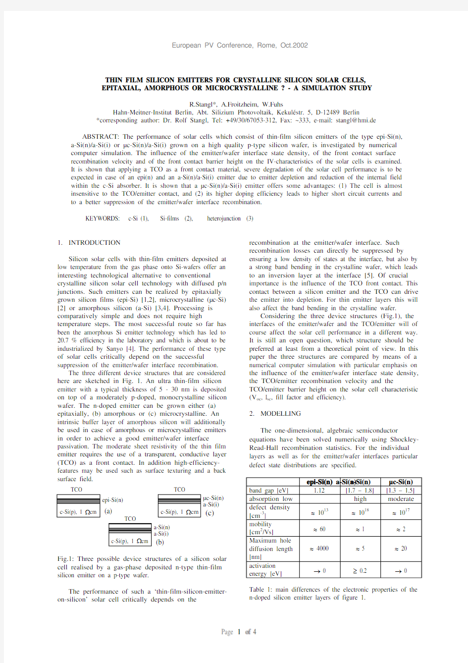
The three different device structures that are considered here are sketched in Fig. 1. An ultra thin-film silicon emitter with a typical thickness of 5 - 30 nm is deposited on top of a moderately p-doped, monocrystalline silicon wafer. The n-doped emitter can be grown either (a) epitaxially, (b) amorphous or (c) microcrystalline. An intrinsic buffer layer of amorphous silicon will additionally be used in case of amorphous or microcrystalline emitters in order to achieve a good emitter/wafer interface passivation. The moderate sheet resistivity of the thin film emitter requires the use of a transparent, conductive layer (TCO) as a front contact. In addition high-efficiency-features may be used such as surface texturing and a back surface field.
Fig.1: Three possible device structures of a silicon solar cell realised by a gas-phase deposited n-type thin-film silicon emitter on a p-type wafer.
The performance of such a ‘thin-film-silicon-emitter-on-silicon’ solar cell critically depends on the recombination at the emitter/wafer interface. Such recombination losses can directly be suppressed by ensuring a low density of states at the interface, but also by
a strong band bending in the crystalline wafer, which leads
to an inversion layer at the interface [5]. Of crucial importance is the influence of the TCO front contact. This
contact between a silicon emitter and the TCO can drive
the emitter into depletion. For thin emitter layers this will
also affect the band bending in the crystalline wafer.
Considering the three device structures (Fig.1), the interfaces of the emitter/wafer and the TCO/emitter will of
course affect the solar cell performance in a different way.
It is still an open question, which structure should be preferred at least from a theoretical point of view. In this
paper the three structures are compared by means of a numerical computer simulation with particular emphasis on
the influence of the emitter/wafer interface state density,
the TCO/emitter recombination velocity and the
TCO/emitter barrier height on the solar cell characteristic
(V
2.MODELLING
The one-dimensional, algebraic semiconductor equations have been solved numerically using Shockley-
Read-Hall recombination statistics. For the individual
layers as well as for the emitter/wafer interfaces particular
defect state distributions are specified.
epi-Si(n)
epi-Si(n) a-Si(n)
a-Si(n) μc-Si(n) oc
, I sc, fill factor and efficiency).
band gap [eV] 1.12 [1.7 – 1.8] [1.3 – 1.5] absorption low high
moderate defect density
[cm-3] ≈ 10
13≈ 1018≈ 1017
mobility
[cm2/Vs] ≈ 60 ≈ 1 ≈ 2
Maximum hole
diffusion length
[nm]
≈ 4000 ≈ 5 ≈ 20
activation
energy [eV] → 0 ≥ 0.2 → 0
Table 1: main differences of the electronic properties of the
n-doped silicon emitter layers of figure 1.
72.1=In order to compare the three different device structures of Fig. 1 the total emitter thickness of epi-Si(n), a-Si(n)/a-Si(i) or μc-Si(n)/a-Si(i) is kept constant at 10 nm if not stated otherwise. If there is an intrinsic buffer layer, the thickness of the intrinsic layer is assumed to be equal to the thickness of the doped layer (5 nm if not stated otherwise). The TCO front contact is modelled by specifying the TCO/emitter surface recombination velocity front and the TCO/emitter barrier height front . A reflection and absorption loss of 20% of the incident solar radiation is assumed, which is a typical value of flat substrates (no surface texturing) together with a TCO thickness of 80 nm. If not stated otherwise, there is no back surface field.
S φFor the crystalline c-Si(p) absorber, a doping concentration of and a constant defect state distribution of was assumed. This corresponds to a high quality FZ wafer (1 ?cm) with a minority carrier diffusion length of , a value which is larger than the wafer thickness of 300 μm.
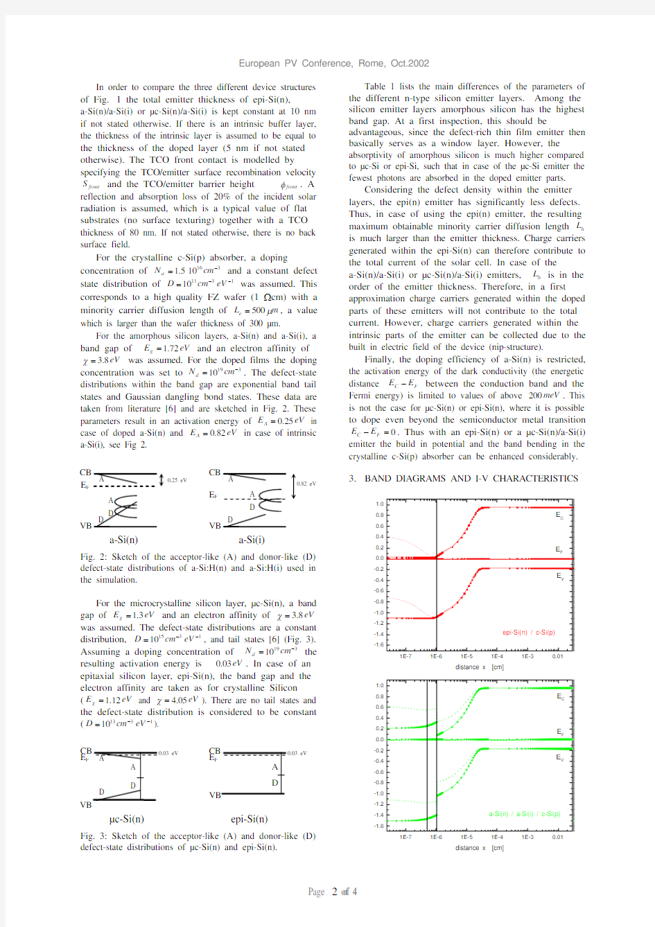
31610 5.1?=cm N a 1311 10??=eV cm D m L e μ 500=For the amorphous silicon layers, a-Si(n) and a-Si(i), a band gap of g and an electron affinity of eV E eV 8.3=χ was assumed. For the doped films the doping concentration was set to . The defect-state distributions within the band gap are exponential band tail states and Gaussian dangling bond states. These data are taken from literature [6] and are sketched in Fig. 2. These parameters result in an activation energy of in case of doped a-Si(n) and in case of intrinsic a-Si(i), see Fig 2.
31910 ?=cm N d eV E A 25.0=eV E A 82.0=
Fig. 2: Sketch of the acceptor-like (A) and donor-like (D) defect-state distributions of a-Si:H(n) and a-Si:H(i) used in the simulation.
For the microcrystalline silicon layer, μc-Si(n), a band gap of and an electron affinity of eV E g 3.1=eV 8.3=χ was assumed. The defect-state distributions are a constant distribution, , and tail states [6] (Fig. 3). Assuming a doping concentration of the resulting activation energy is . In case of an epitaxial silicon layer, epi-Si(n), the band gap and the electron affinity are taken as for crystalline Silicon ( and 1315 10??=eV cm D 31910?=cm N d eV 03.0eV E g 12.1=eV 05.4=χ). There are no tail states and the defect-state distribution is considered to be constant (1).
313 10??=eV cm D
Fig. 3: Sketch of the acceptor-like (A) and donor-like (D) defect-state distributions of μc-Si(n) and epi-Si(n). Table 1 lists the main differences of the parameters of the different n-type silicon emitter layers. Among the silicon emitter layers amorphous silicon has the highest band gap. At a first inspection, this should be advantageous, since the defect-rich thin film emitter then basically serves as a window layer. However, the absorptivity of amorphous silicon is much higher compared to μc-Si or epi-Si, such that in case of the μc-Si emitter the fewest photons are absorbed in the doped emitter parts.
Considering the defect density within the emitter layers, the epi(n) emitter has significantly less defects. Thus, in case of using the epi(n) emitter, the resulting maximum obtainable minority carrier diffusion length h is much larger than the emitter thickness. Charge carriers generated within the epi-Si(n) can therefore contribute to the total current of the solar cell. In case of the a-Si(n)/a-Si(i) or μc-Si(n)/a-Si(i) emitters, h is in the order of the emitter thickness. Therefore, in a first approximation charge carriers generated within the doped parts of these emitters will not contribute to the total current. However, charge carriers generated within the intrinsic parts of the emitter can be collected due to the built in electric field of the device (nip-structure).
L L Finally, the doping efficiency of a-Si(n) is restricted, the activation energy of the dark conductivity (the energetic distance F C between the conduction band and the Fermi energy) is limited to values of above . This is not the case for μc-Si(n) or epi-Si(n), where it is possible to dope even beyond the semiconductor metal transition . Thus with an epi-Si(n) or a μc-Si(n)/a-Si(i) emitter the build in potential and the band bending in the crystalline c-Si(p) absorber can be enhanced considerably.
E E ?meV 2000=?
F C E E
3. BAND DIAGRAMS AND I-V CHARACTERISTICS
-1.6
-1.4-1.2-1.0-0.8-0.6-0.4-0.20.00.20.40.6
0.81.0
e n e r g y [e V ]
distance x [cm]
1E-7
1E-6
1E-5
1E-4
1E-3
0.01
-1.6
-1.4-1.2
-1.0-0.8-0.6-0.4-0.20.00.2
0.40.60.8
1.0 e n e r g y [e V ]
distance x [cm]
CB A
0.25 eV
E F
0.82 eV
A E F D D
VB
a-Si(n) a-Si(i)
E CB 0.03 eV
μc-Si(n) A
D
D VB
F E CB 0.03 eV
A A D
VB
F
epi-Si(n)
1E-7
1E-6
1E-5
1E-4
1E-3
0.01
-1.6
-1.4-1.2-1.0-0.8-0.6-0.4-0.20.00.2
0.40.60.81.0
e n e r g y [e V ]
distance x [cm]
Fig. 4: Band profiles of the three different device structures. With respect to the TCO/emitter front contact, the band diagrams are calculated under zero barrier height (flatband conditions, straight lines) and assuming a barrier height of 0.4 eV (emitter depletion, dotted lines). The position is given in logarithmic scale, the TCO contact is on the left at x=0 cm, the Fermi energy was set to 0 eV on the energetic scale.
Fig.4 displays the resulting band profiles for the three device structures. In a first approximation, additional interface defects at the emitter/wafer interface have been neglected. Further assumptions are flat band conditions () and a high recombination velocity (S eV front 0=φfront = 107 cm/s) at the TCO/emitter interface. Also shown is the influence of a positive front contact barrier height of , which drives the emitter into depletion. eV front 4.0=φ
c u r r e n t
d
e n s i t y [m A /c m 2
]
voltage [V]
Fig. 5: Simulated I-V curves of ‘thin-film-silicon- emitter-on-p-doped silicon’ solar cells with epi-Si(n), μc-Si(n)/a-Si(i) and a-Si(n)/a-Si(i) emitters on flat substrates (reflection loss of 20 %) and without back surface field. The curves are calculated for zero barrier height (flatband conditions, straight lines) and for a barrier height of 0.4 eV (emitter depletion, dotted lines) at the TCO/emitter front contact.
Fig. 5 displays the simulated I-V characteristics under illumination with AM 1.5 light. The resulting cell efficiencies exceed 16 % for all device structures. If high efficiency features were taken into account including a back surface field and only 3 % reflection loss the resulting efficiencies would exceed 21 %.
Four characteristic features are observed which remain, even if the defect density at the emitter/wafer interface and/or the front contact barrier height at the TCO/emitter interface is varied: (1) The solar cell efficiency is always highest for the μc-Si(n)/a-Si(i) emitter. (2) Under variation of the front contact barrier height the IV-characteristic does not change significantly in case of the μc-Si(n)/a-Si(i) emitter, whereas the solar cell efficiency degrades significantly for higher barrier heights in case of the epi-(n) and a-Si(n)/a-Si(i) emitters. (3) The short-circuit current decreases in the sequence from epi-Si(n) to μc-Si(n)/a-Si(i) and to a-Si(n)/a-Si(i). (4) The open-circuit voltage is significantly reduced for the epi-Si(n) emitter. The physical origin of this features will now be examined in more detail.
The reason for the trend in the decrease of the short-circuit current is simple: Most photons absorbed in the epi-Si(n) emitter will contribute to the short-circuit current, whereas the doped parts of the other two emitters are electrically dead in first approximation. Due to the higher built-in-potential of the μc-Si(n)/a-Si(i) emitter compared to the a-Si(n)/a-Si(i) emitter more charge carriers generated in the emitter will be collected in case of the μc-Si(n)/a-Si(i) emitter. In order to explain the other three characteristic features mentioned above, the influence of the emitter/wafer interface and of the TCO/emitter interface on the solar cell performance has to be discussed in more detail for all three emitter types.
4. EMITTER/WAFER INTERFACE STATE DENSITY
Interface states at the emitter/wafer interface will significantly reduce the open-circuit voltage of the solar cell (Fig. 6). A constant interface state distribution throughout the c-Si band gap has been used for simulation. The reduction in open-circuit voltage is due to additional interface recombination and can be partially suppressed by ensuring a strong band bending in the crystalline c-Si(p) absorber, as shown in [5], [7] for an a-Si(n)/a-Si(i) emitter. In any case, it is essential to passivate the emitter/wafer interface in a way that defect densities not larger than N trap = 1012 cm -2 are achieved (see Fig. 6). This appears possible making use of the excellent passivation that can be achieved with an a-Si(i) buffer layer [8].
1E10
1E11
1E12
1E13
1E14
1E15
o p e n c i r c u i t v o l t a g e V O C [V ]
emitter/wafer interface state density N trap [cm -2
]
Fig. 6: Dependence of the open-circuit voltage V OC on the emitter/wafer interface state density for epi-Si(n), μc-Si(n)/a-Si(i) and a-Si(n)/a-Si(i) emitters.
TCO/EMITTER SURFACE RECOMBINATION VELOCITY
Good surface passivation of the TCO/emitter surface is only necessary in case of the epi-Si(n) emitter (see Fig. 7). If the front surface recombination velocity is reduced from S front = 107 cm/s to 103 cm/s, a higher open-circuit voltage
can be obtained only in case of the epi-Si(n) emitter. This is due to the fact that the doped parts of the μc-Si(n)/a-Si(i) and the a-Si(n)/a-Si(i) emitters are electrically dead especially close to the TCO/emitter interface. The short-circuit current and fill factor remain essentially unchanged for all emitter types.
10
10010001000010000010000001E7
o p e n c i r c u i t v o l t a g e V O C [V ]
TCO/emitter surface recombination velocity S front [cm/s]
Fig. 7: Dependence of the open-circuit voltage V OC on the TCO/emitter surface recombination velocity for epi-Si(n), μc-Si(n)/a-Si(i) and a-Si(n)/a-Si(i) emitters.
5. CO/EMITTER BARRIER HEIGHT
T
According to Andersons model, the TCO/emitter contact will always drive the emitter into depletion [7]. This has also been investigated experimentally in case of the TCO/a-Si(n) contact [9]. According to this work the TCO/emitter front contact barrier height is expected to be somewhere in the range 0.2 – 0.4 eV depending on the value of the TCO work function and the type of contact.
e f f i c i e n c y [%]
TCO/emitter barrier height φfront [eV]
(n)/a-Si(i) and a-Si(n)/a-Si(i) emitters.
to the decrease in s order to minimize absorption losses in the emitter layers.
6. ONCLUSION
d of charg
e carriers, which are absorbed within the emitter.
[1] a), 61. [2] mmonte,
[3] , J.H.Werner,
[4] i, S.Kiyama, Proc. 20th IEEE PVSEC [5] r, W.Fuhs, Proc. 17th
[6] lls, Kluwer [7]
oc. 29th IEEE PVSEC (2002, New [8] Proc. 29 IEEE
[9] t, W.Fuhs, Proc. 17th EUR PVSEC, (2001, Munich).
Fig. 8: Dependence of the solar cell efficiency on the TCO/emitter barrier height of epi-Si(n), μc-Si
Again, for the μc-Si(n)/a-Si(i) emitter, the solar cell efficiency remains approximately unaffected by the TCO/emitter barrier height (see Fig. 8). With an a-Si(n)/a-Si(i) emitter, mainly the fill factor but also the open-circuit voltage decreases. For the epi-Si(n) emitter there is a slight decrease of the open-circuit voltage and also of the short-circuit current. This leads olar cell efficiency as shown in Fig. 8.
If the doped part of the emitter is thick enough, the free carriers of the emitter will be sufficient to shield the electric field imposed by the TCO/emitter front contact barrier height. This will only affect the solar cell performance in case of the epi-Si(n) emitter, since the doped parts of the μc-Si(n)/a-Si(i) and the a-Si(n)/a-Si(i) emitters are electrically dead. However, if the emitter is sufficiently thin, additional carriers from the absorber and recharged defects from the emitter have to be used in order to shield the electric field. This will considerably alter the band bending in the crystalline c-Si(p) absorber of the solar cell, and lead to a strong decrease of the fill factor and the open-circuit voltage. With an emitter thickness of nm 10, this critical value for the thickness has already been reached in case of the a-Si(n)/a-Si(i) emitter, but not in case of the epi-Si(n) or the μc-Si(n)/a-Si(i) emitters (see Fig.4 for comparison). The reason for this is the limitation of the doping efficiency of a-Si(n). Therefore, for reasonably thin emitter layers in the range of 3 – 30 nm, only the μc-Si(n)/a-Si(i) emitter is insensitive to the TCO/emitter barrier height. Note that a reasonably thin emitter is required for good solar cell performance in
C
The simulation study leads to detailed insight into the physical background and limitations of ‘thin-film-silicon-emitter-on-p-doped silicon’ solar cells using gas-phase deposited emitters of the type epi-Si(n), μc-Si(n)/a-Si(i) and a-Si(n)/a-Si(i). It turns out hat excellent emitter/wafer interface passivation which leads to defect densities of less than N trap = 1012 cm -2 is of crucial importance. With the exception of the μc-Si(n)/a-Si(i) emitter, a positive TCO/emitter barrier height, which is to be expected using a TCO/thin film silicon contact, severely degrades the solar cell performance. In particular for the epi-Si(n) emitter the TCO/emitter surface recombination velocity has to be
controlled (S front ≤ 104
cm/s). This simulation study suggests that the μc-Si(n)/a-Si(i) emitter may have some advantages over the other choices: (1) This emitter is insensitive to the TCO/emitter front contact and (2) the high doping efficiency of μc-Si(n) leads to a stronger band bending in the absorber. The latter may result in a pronounced reduction of the emitter/absorber interface recombination and also to a higher yiel REFERENCES
K.Lips, J.Platen, S.Christiansen, I.Sieber, L.Elstner,
W.Fuhs, Proc.28th IEEE PVSEC (2000, Alask R.Rizzoli, E.Centurioni, J.Pla, C.Su A.Migliori, A.Desalvo, F.Zignani,
J.Non-Cryst.Solids, 299-302 (2002) 1203. N.Jensen, R.M.Hausner, R.B.Bergmann U.Rau, Prog.Photovolt., 10, (2002), 1. H.Sakata, T.Nakai, T.Baba, M.Taguchi, S.Tsuge,
K.Uchihash (2000), 7. R.Stangl, A.Froitzheim, L.Elstne EUR PVSEC, (2001, Munich).
R.Schropp, M.Zeman, Amorphous and
Microcrystalline Silicon Solar Ce Academic Publishers (1998). A.Froitzheim, R.Stangl, L.Elstner, M.Schmidt,W.Fuhs, Pr Orleans).
S.Dauwe, J.Schmidt, R.Hetzel, th PVSEC (2002, New Orleans).
M.Schmidt, A.Froitzheim, R.Stangl, L.Elstner,
K.Kliefoth, W.Füssel, M.Schmid
玻璃钢制作工艺
精心整理 玻璃钢制作工艺流程 首先在制作好的模具清理表面的垃圾灰尘,打好8#蜡,刷上一层“33#胶衣”的东西,表面光滑,就是这个胶衣的效果,等它干了后,就开始用调配好的玻璃钢树脂和玻璃纤维毡开始“积层”。(其中调配玻璃钢树脂是根据其产品的强度和耐火程度来调配,还要添加一些固化剂,钴水之类的)。玻璃钢第一层积完,等它干了后,再用纤维布继续往下积层,一般强度的:纤维布积4到5层就足够,积的过程是积1到2层就要等干一次大约大半个小时。积层:是一边用刷子蘸玻璃钢树脂涂在就起模,来的。 然一、生产准备工序 设备、工装、工具等生产装备明细: 1.玻璃钢模具 2.铲刀 3.毛刷
4.吹尘枪 5.干净毛巾 6.海绵 7.8#黄蜡 8.树脂 9.玻璃纤维 10.胶衣 11. A. B. C. D.应用铲 .清 E. 5--20 匀, F. 干净, A. 工使用面。 B.在用干净毛巾进行擦拭蜡层作业时,应将保留在模具面上的蜡层彻底清除干净并将模具抛光亮,以免多次在模具面上积蜡造成蜡层擦拭不掉形成蜡垢,从而导致模具哑光和影响产品脱模和表面效果。 二.涂刷胶衣层工序 设备工装工具等生产装备明细
1.玻璃钢模具 2.毛刷 3.水瓢 4.胶衣 5.固化剂 6.温度计 生产加工工艺 A. B. C.. D. E. 执行。 A. B. C. 三.定型铲泡工序 设备工装工具等生产装备明细: 1.玻璃钢模具 2.玻璃纤维腻子 3.固化剂 4.刮板或灰刀
5.毛刷 6.水瓢 7.02#玻璃纤维布 8.191#树脂 9.铲刀或刀片 10.60#--240#砂布 生产加工工艺: A. B. , C. 02# D. 具面. A. B. C. 四.增强层制作工序 设备工装工具等生产装备明细: 1.玻璃钢模具 2.毛刷 3.水瓢 4.191#树脂
玻璃工艺品的制作方法
玻璃工艺品的制作方法 玻璃主要成份是矽砂、苏打灰、碳酸钠、碳酸钾、石灰及铝土、铅丹等,种类很多。一般主要成份为钠玻璃属之;钾玻璃,制瓶玻璃属之;铅玻璃,仪器玻璃属之。新竹地区的矽石出产于关西一带,但近年来铁份含量偏高,品质稍差,所以大多仍由澳洲及马来西亚进口。首先先矽砂、石灰、苏打灰等放入坩锅窑中,在一千四百五十摄氏度的高温下十六小时,待混合融解成浓稠液体后,臵于模具上,使之成形,再经十二小时徐冷后加式处理。期间施以喷沙、添色、嵌入金箔、磨花、雕刻、药水浸泡等装饰技巧。又在烧制时使用各种金属发色剂,制作出来的玻璃刚具有不同的颜色。 玻璃艺吕的成形法: 玻璃一般玻璃原料燃烧溶解后都形成液体粘稠液,要使其冷却成形,大都采用型吹法,使用各种材质的模型,如木材、粘土、金属等预先制成所需要的型器,把融化的玻璃液倒入模型内,待冷却后再将模型打开即成,一般用于吹玻璃无法制成的器具,大部分的工厂都采用此种方法,可以大量生产。 另一种为吹气成型法,即吹玻璃,就是取出适量的玻璃溶液,放于铁吹管的一端,一面吹气,一面旋转,并以熟练的技法,使用剪刀或钳子,使其成型。 常用技法 冷工制作法 1.彩绘以彩绘颜料,在室温下于玻璃物表面描绘图画,有些需加热固定,有些则不需。过程中也可以加上金箔、银箔熔成的金属颜料,称为饰金彩绘。 2.釉彩是一种需要再加温的彩绘声绘色的技法,在玻璃物表面,以釉彩颜料绘制图样,然后再臵入熔炉加温固定颜料,避免剥落。 3.镶嵌以有凹槽之铅条为线框架,组合成千上万片的彩色玻璃板的技法,需绘制小型平面图,根据平面图绘制等尺寸的草图,确定每一种颜色的造型与尺寸,正确切割玻璃板,以铅线熔焊成大块面镜。 4.版画无须加温的冷作,利用喷砂或磨刻的技法,将图刻印在玻璃板上,加以制版,以版画机或滚筒上色,在棉纸或水彩纸上压制成版画。 5.浮雕在双层或多层颜色套料的玻璃,浮雕出立体图案透露出底色,形成浮雕效果。 6.切割运用切割轮,在玻璃物上切割纹饰、块面,线条等装饰,或大面切割成造型,有时双色套料玻璃,因表现内外不同的颜色的特殊效果。 7.磨刻以钻石或金属雕刻,或雕刻笔等雕刻工具在玻璃表面画线装饰花纹与图样的技法,因使用工具的不同,可分为轮刻、点刻、平刻等种技法。 8.酸蚀在玻璃板绘制图形、勾勒线条,再经化学酸剂分阶段蚀出深浅不同的图案。 9.喷砂先以胶带粘满整个玻璃物,在以刻刀镀刻去掉图案不要的部分,臵入喷砂机,运用金刚砂的高喷射力,在玻璃上做出雾状效果。 10.研磨以旋转轮盘为研磨台,混合水与金刚砂,磨平刨光玻璃作品。 11.刨光以旋转皮轮为平台,将玻璃至于其上,磨光刨光大块平面。
新译林牛津小学英语六年级上册江苏省省优质公开课赛课 Unit 7 Protect the Earth
Unit 7 Protect the Earth (Story time) (江苏省优质课评比教案) Step1: Pre-reading 1.Lead-in T: Good morning, boys and girls. Ss: Good morning, Miss Zheng. T: I’m very happy to be your teacher today. I hope we can enjoy this lesson. OK? Ss: OK. T: Thank you. As you kno w I’m from… Ss: Yancheng. T: Yes. It is a very beautiful city. There are some rare wild animals in Yancheng. Can you guess what are they? Ss: They are… (展示丹顶鹤和麋鹿的图片问学生) T: Look, They are red-crowned cranes and milu deers. They live happily in Yancheng. Today I bring you a short story about an animal. Look, what’s this? S: It’s a bird. T: Yes. Let’s watch the cartoon. After watching it, please tell me: What can you see in the cartoon? T: What can you see in the cartoon? S: I can see a river? T: Is the river clean? S: No, it’s dirty. …… T: What can you feel about the cartoon? S: … T: Yes. There are so many bad things. Who did these bad things? Ss: People. T: What do you want to say to these people? Ss: … T: Yes. We should protect the Earth, right? Ss: Yes. T: So t oday we’re going to learn Unit 7 Protect the Earth. (揭题,带领学生读课题)
玻璃生产工艺流程图
玻璃生产工艺流程图 玻璃是如何生产出来的呢?这个问题对于专家来说可能很简单,但是对于普通的消费者来说可能还是有了解的兴趣的,今天,我们和中华包装瓶网的小编一起去简要的了解一下。玻璃的生产工艺包括:配料、熔制、成形、退火等工序。分别介绍如下: 1.配料,按照设计好的料方单,将各种原料称量后在一混料机内混合均匀。玻璃的主要原料有:石英砂、石灰石、长石、纯碱、硼酸等。 2.熔制,将配好的原料经过高温加热,形成均匀的无气泡的玻璃液。这是一个很复杂的物理、化学反应过程。玻璃的熔制在熔窑内进行。熔窑主要有两种类型:一种是坩埚窑,玻璃料盛在坩埚内,在坩埚外面加热。小的坩埚窑只放一个坩埚,大的可多到20个坩埚。坩埚窑是间隙式生产的,现在仅有光学玻璃和颜色玻璃采用坩埚窑生产。另一种是池窑,玻璃料在窑池内熔制,明火在玻璃液面上部加热。玻璃的熔制温度大多在1300~1600゜C。大多数用火焰加热,也有少量用电流加热的,称为电熔窑。现在,池窑都是连续生产的,小的池窑可以是几个米,大的可以大到400多米。 3.成形,是将熔制好的玻璃液转变成具有固定形状的固体制品。成形必须在一定温度范围内才能进行,这是一个冷却过程,玻璃首先由粘性液态转变为可塑态,再转变成脆性固态。成形方法可分为人工成形和机械成形两大类。 A.人工成形。又有(1)吹制,用一根镍铬合金吹管,挑一团玻璃在模具中边转边吹。主要用来成形玻璃泡、瓶、球(划眼镜片用)等。(2)拉制,在吹成小泡后,另一工人用顶盘粘住,二人边吹边拉主要用来制造玻璃管或棒。(3)压制,挑一团玻璃,用剪刀剪下使它掉入凹模中,再用凸模一压。主要用来成形杯、盘等。(4)自由成形,挑料后用钳子、剪刀、镊子等工具直接制成工艺品。 B.机械成形。因为人工成形劳动强度大,温度高,条件差,所以,除自由成形外,大部分已被机械成形所取代。机械成形除了压制、吹制、拉制外,还有(1)压延法,用来生产厚的平板玻璃、刻花玻璃、夹金属丝玻璃等。(2)浇铸法,生产光学玻璃。(3)离心浇铸法,用于制造大直径的玻璃管、器皿和大容量的反应锅。这是将玻璃熔体注入高速旋转的模子中,由于离心力使玻璃紧贴到模子壁上,旋转继续进行直到玻璃硬化为止。(4)烧结法,用于生产泡沫玻璃。它是在玻璃粉末中加入发泡剂,在有盖的金属模具中加热,玻璃在加热过程中形成很多闭口气泡这是一种很好的绝热、隔音材料。此外,平板玻璃的成形有垂直引上法、平拉法和浮法。浮法是让玻璃液流漂浮在熔融金属(锡)表面上形成平板玻璃的方法,其主要优点是玻璃质量高(平整、光洁),拉引速度快,产量大。 4.退火,玻璃在成形过成中经受了激烈的温度变化和形状变化,这种变化在玻璃中留下了热应力。这种热应力会降低玻璃制品的强度和热稳定性。如果直接冷却,很可能在冷却过程中或以后的存放、运输和使用过程中自行破裂(俗称玻
新译林牛津小学英语六年级上册优质公开课赛课教案 6A Unit8 Chinese New Year period2
U8 Grammar & Fun time 教学目标: 掌握一般将来时的句式结构,能用一般将来时谈论自己的节日安排。 教学重难点: 1、句型be going to …的用法。 2、介词in 、at在节日名称前的用法区别。 教学过程: Step 1 Revision 1、Say the words and phrases.映示课文插图,说出相应单词及 词组。 2、T:What is Su Hai going to do ? Guess!根据香港和大陆人的 节日习俗有所不同,来猜测苏洋的节日安排。 3、T: Chinese New Year is a popular holiday in China. What are you going to do this Chinese New Year ? I’m going to …(板书) 4、Practice in each group of four .指名学生提问:What is he/she
going to do ? He/She is going to …What are they going to do ? They are going to … Step 2 Grammar time 1、T: Let’s read the sentences. 呈现Grammar time中的句子,以问答形式朗读。 2、生试总结一般将来时的句式特点。 3、教师总结。 ⑴一般将来时表示在将来某一时间将要发生的动作或存在的状态,也可表示将来某一段时间内经常发生的动作或存在的状态。 ⑵结构:be going to + 动词原形 What is he going to do at Chinese New Year ? He is going to watch a lion dance . What are you going to do on Chinese New Year’s Eve ? We’re going to have a big dinner . 3、Practice . ⑴我打算明天打扫我的房间。 I ____ going to____ my bedroom tomorrow. ⑵他这个周末准备去拜访他的祖父母。
玻璃制作工艺流程
材质 玻璃器皿多用钠钙硅酸盐玻璃做成。无色透明的器皿,玻璃中的含铁量一般低于%。在玻璃原料中加入着色剂,可制得有色玻璃;加入乳浊剂,制得乳浊玻璃(见玻璃制造)。 制造琢磨车刻的高级艺术器皿如高脚杯、香水瓶、果盆等多采用钾铅硅酸盐玻璃,又称铅晶质玻璃。这种玻璃含PbO,具有高折射率和色散,磨刻棱面时格外光亮,高比重,敲击时发清脆声响。 含PbO30%以上的为全铅晶质玻璃,含PbO24~30%为中铅晶质玻璃,含PbO18%以下为低铅晶质玻璃。 另外还有含BaO的钡晶质玻璃。 煮食器皿如咖啡壶等制品采用耐热硼硅酸盐玻璃,其热膨胀系数低,耐温度急变性强。 成型 将按玻璃成分配合的粉料和熟料投入坩埚窑或池窑(见玻璃熔窑)中熔制,熔化后,澄清成均匀无气泡、无结石、无条纹的玻璃液,再冷却至适应相应成型方法要求的粘度范围,进行各种成型操作。 吹制成型 有人工和机械吹制成型两种方式。人工成型时,手持吹管从坩埚内或池窑取料口处挑料,在铁模或木模中吹成器形。光滑圆形制品用转吹法;表面有凸凹图案花纹或形状不成圆形的制品用静吹法。先挑无色料吹成小泡,再用小泡挑颜色料或乳浊料吹成器形的称为套料吹制。用颜色易熔料粒沾在乳浊套料上,各色自然熔流,可吹成自然景器皿;在颜色料上沾带状乳浊料,可吹成拉丝器皿。机械成型用于吹制大批量制品。吹制机受料后自动合铁模吹成器形,脱模后去除帽口即成器皿。还可采用压-吹成型,先将料冲成小泡(雏形),再继续吹制成器形。它比单纯用吹制机吹制效率高,质量好。 压制成型 人工成型时,人工挑料剪入铁模,驱动冲头,压成器形,凝固定型后脱模。机械成型自动化生产,批量大,效率高。压制成型适用于能退出冲头的口大底小器形制品,如杯、盘、烟缸等。 离心成型 受料在旋转的模子内,由于旋转产生的离心力使玻璃展开并紧贴模子,凝固定型后取出。适宜于器壁均匀的大型玻璃器皿的成型。 自由成型 又称无模成型。用人工挑料在窑前反复烘烤修饰或热粘结。由于不与模子接触,玻璃表面光亮,制品形状线条光滑。制成品又称窑玻璃制品。
牛津小学英语公开课
《义务教育课程标准实验教科书?牛津小学英语》6B 第二单元第一教时 河口镇孔堤口小学吕永中 教学内容:牛津小学英语6B 第二单元第一教时Unit 2 More exercise(part A ) 教学目标: 1、能正确地听,说,读,写单词和词组more ,be good at ,slower, player, true, ball game. 2、能正确地听,说,读,写句型Ben runs faster than Jim. Does Jim swim slower than his friends? Yes,he does./ No,he doesn’t. 3、能正确地运用对话中的日常交际用语和三会句型That’s true. Mike runs as fast as Ben. 4、能正确地理解,掌握对话内容并能朗读初步表演对话。 5、能运用本课所学语言进行“体育锻炼”的对话交际。 教学重点: 1、能正确地听,说,读,写句型Ben runs faster than Jim. Does Jim swim slower than his friends? Yes,he does./ No,he doesn’t. 2、能正确理解、掌握对话内容,并能朗读,尝试表演对话。 教学难点: 1、能正确理解、掌握对话内容,并能朗读,尝试表演对话。 2、be good at 和do well in 后面接动名词。 课前准备: 1、教具准备:一套多媒体课件, 练习作业。 2、板书准备:预先写好课题Unit 2 More exercise,贴好表格、表格内的内容贴纸。 教学主流程: Step1 Warming –up. 1. Greetings. T: 用Hello, boys and girls. Do you like sport?I like running. Do you like running?…… 2. Riddles. T: Would you like to play a game? I describe a person, you guess who he is. Now listen carefully: He is a runner. He runs very fast. He is tall. He is a Chinese man. Who is he? S: He is Liu Xiang. T: Yes, what does he like? S: He likes running. He likes to run. T: Yes, he can run fast, so he is good at running. How about you? S: I like playing basketball. T: Do you play well? S: Yes, I do. T: So you are good at basketball. (板书出示:be good at ) T: I am good at singing. Liu Xiang is good at running. S is good at basketball. So we are good at PE. Who are not good at PE?(some students hands up) T: Oh, you should do more exercise. (揭示课题Unit 2 More exercise) Some students are not good at PE. They should do more exercise. And they’ll do better in PE. (板书出示:do more
玻璃生产工艺及生产流程
玻璃生产工艺及生产流程 玻璃生产工艺 1、原料预加工。将块状原料(石英砂、纯碱、石灰石、长石等)粉碎,使潮湿原料干燥,将含铁原料进行除铁处理,以保证玻璃质量。 2、配合料制备。根据产品的不同,配合料的组成略有区别。例如普通浮法玻璃的配合料(按照50公斤计算),需要消耗石英砂33.55公斤、石灰石2.96公斤、白云石8.57公斤、纯碱11.39公斤、芒硝0.55公斤、长石3.45公斤、碳粉0.03公斤。 3、熔制。玻璃配合料在池窑或坩埚窑内进行高温(1550-1600度)加热,使之形成均匀、无气泡并符合成型要求的液态玻璃。 4、成型。将液态玻璃加工成所要求形状的制品,如平板玻璃、各种器皿等。 5、热处理。通过退火、淬火等工艺,消除或产生玻璃内部的应力、分相或晶化,以及改变玻璃的结构状态。 浮法玻璃生产线流程图 通平板玻璃与浮法玻璃的区别 普通平板玻璃与浮法玻璃都是平板玻璃,区别在于生产工艺、品质上不同。
1、生产工艺方面。普通平板玻璃是将原料按一定比例配制,经熔窑高温熔融,通过垂直引上法或平拉法、压延法生产出来的透明无色的平板玻璃。浮法玻璃是将原料按一定比例配制,经熔窑高温熔融,玻璃液从池窑连续流出并浮在金属液面上,摊成厚度均匀平整、经过抛光的玻璃带,冷却硬化后脱离金属液,再经退火切割而成的透明无色平板玻璃。 2、在品质方面。普通平板玻璃按外观质量分为优等品、一等品、合格品三类;按厚度分为2、 3、 4、 5、6mm等厚度。普通玻璃呈现翠绿色,易碎、透明度不高,雨淋暴晒下易老化变形。浮法玻璃按外观质量分为优等品、一等品、合格品三类;按厚度分为2、3、4、5、 6、8、10、12、15、19mm等厚度。浮法玻璃表面平滑无波纹,透视性佳,具有一定韧性。 浮法玻璃的生产工艺 下面以国内普通的日熔化量600吨的生产线为例,介绍浮法玻璃的制造流程。 整个生产线长度约有500米,每天可生产550到600吨的玻璃,也就是相当于3米宽、3毫米厚、长度约25公里的玻璃带。一旦开始生产,便是每天24小时不间断,直到大约8-10年之后才会停炉维修。浮法玻璃是在锡槽中制造。浮 法生产是当今平板玻璃主要的生产方式,其流程可分为以下五个阶段: 1、原料的混成。 浮法玻璃的主要原料成份有:73%的二氧化硅、9%的氧化钙、13%的碳酸钠及4%的镁。这些原料依照比例混合,再加入回收的碎玻璃小颗粒。 2、原料的熔融。 将调配好的原料经过一个混合仓后,再进入一个有5个仓室的窑炉中加热,约1550摄氏度时成为玻璃融液。 3、玻璃成型。 玻璃熔液流入锡槽且浮在熔化的金属锡液之上,此时温度约1000摄氏度。 在锡液上的玻璃熔液形成宽3.66米、厚度介于3mm至19mm的玻璃带。因为 玻璃与锡有极不相同的粘稠性,所以浮在上方的玻璃熔液与下方的锡液不会混合在一起,并且形成非常平整的接触面。 4、玻璃熔液的冷却。
玻璃制作工艺
玻璃 玻璃是非晶无机非金属材料,一般是用多种无机矿物(如石英砂、硼砂、硼酸、重晶石、碳酸钡、石灰石、长石、纯碱等)为主要原料,另外加入少量辅助原料制成的。它的主要成分为二氧化硅和其他氧化物。普通玻璃的化学组成是Na2SiO3、CaSiO3、SiO2或Na2O·CaO·6SiO2等,主要成分是硅酸盐复盐,是一种无规则结构的非晶态固体。广泛应用于建筑物,用来隔风透光,属于混合物。另有混入了某些金属的氧化物或者盐类而显现出颜色的有色玻璃,和通过物理或者化学的方法制得的钢化玻璃等。有时把一些透明的塑料(如聚甲基丙烯酸甲酯)也称作有机玻璃。 玻璃的生产工艺包括:配料、熔制、成形、退火等工序.分别介绍如下: 配料,按照设计好的料方单,将各种原料称量后在一混料机内混合均匀.玻璃的主要原料有:石英砂、石灰石、长石、纯碱、硼酸等. 熔制,将配好的原料经过高温加热,形成均匀的无气泡的玻璃液.这是一个很复杂的物理、化学反应过程.玻璃的熔制在熔窑内进行.熔窑主要有两种类型:一种是坩埚窑,玻璃料盛在坩埚内,在坩埚外面加热.小的坩埚窑只放一个坩埚,大的可多到20个坩埚.坩埚窑是间隙式生产的,现在仅有光学玻璃和颜色玻璃采用坩埚窑生产.另一种是池窑,玻璃料在窑池内熔制,明火在玻璃液面上部加热.玻璃的熔制温度大多在1300~1600゜C.大多数用火焰加热,也有少量用电流加热的,称为电熔窑.现在,池窑都是连续生产的,小的池窑可以是几个米,大的可以大到400多米. 成形,是将熔制好的玻璃液转变成具有固定形状的固体制品.成形必须在一定温度范围内才能进行,这是一个冷却过程,玻璃首先由粘性液态转变为可塑态,再转变成脆性固态.成形方法可分为人工成形和机械成形两大类. A. 人工成形.又有 (1) 吹制,用一根镍铬合金吹管,挑一团玻璃在模具中边转边吹.主要用来成形玻璃泡、瓶、球(划眼镜片用)等.
玻璃加工制作工艺方法及流程
玻璃加工制作工艺方法及流程 1.质量计划目标 (1)所有钢化玻璃均应满足美国ASTMC1048 标准和英国BS6206 标准以及国家《钢化玻璃》(GB/T9963-1998)和《幕墙用钢化玻璃与半钢化玻璃》(GB17841-1999)标准;(2)所有夹层玻璃均应满足澳大利亚AS/NZ2008 标准和英 (GB9962-1999)标准。国BS62006标准以及国家《夹层玻璃》 2.钢化玻璃 (1)加工流程图 切割玻璃磨边倒角 清洗加热至近软化点 包装急速冷却 )钢化玻璃是将普通退火玻璃通过加热到其软化点温度2(经过上述工艺处理后的玻璃,两面吹风急冷后而得到。附近,表面形成了强大均匀的压应力(内部留有等值均匀的张应力)。这种表面压应力可抵御导致玻璃碎的各种张力(如拉伸、弯曲和冲击等),使玻璃机械强度成倍增加。一般钢化.玻璃的表面压力在95MPa 以上,钢化玻璃具有以下特点:机械强度高;机械强度是普通退火玻璃的3 倍左右;
安全性能好:破碎后成钝角小颗粒,对人体不会造成重大伤害; 抗挠强度大:比普通玻璃大3~4 倍; 热稳定性佳:能承受的温差是退火玻璃的2.5~3 倍,最高使用温度接近300OC。 (3)质量控制 主要质量控制项目指标及相关标准序主要质量控制项控制指相关标 -2.0mm3.0mm1钢化玻璃尺寸偏+0.无要22.0mm对角线允许偏孔径和孔位允许1.5mm 3 2.0mm ≤钢化玻璃表面应495MPa95NPa 值按SNB004 标准允许轻爆边边部磨边质量 5 钢化玻璃破碎颗粒≥40 粒≥40 粒6 数钢化玻璃弓形弯曲7 ≤0.1%≤0.5%度≤钢化玻璃破碎颗粒%0.3≤%0.058 数(0.15/300 mm) 钢化玻璃破碎颗粒高于相关国标标9 低于内控数准 (4)生产过程控制 生产过程控制内容及检测
玻璃生产工艺及生产流程
玻璃生产工艺及生产流 程 文件排版存档编号:[UYTR-OUPT28-KBNTL98-UYNN208]
玻璃生产工艺及生产流程 玻璃生产工艺 1、原料预加工。将块状原料(石英砂、纯碱、石灰石、长石等)粉碎,使潮湿原料干燥,将含铁原料进行除铁处理,以保证玻璃质量。 2、配合料制备。根据产品的不同,配合料的组成略有区别。例如普通浮法玻璃的配合料(按照50公斤计算),需要消耗石英砂公斤、石灰石公斤、白云石公斤、纯碱公斤、芒硝公斤、长石公斤、碳粉公斤。 3、熔制。玻璃配合料在池窑或坩埚窑内进行高温(1550-1600度)加热,使之形成均匀、无气泡并符合成型要求的液态玻璃。 4、成型。将液态玻璃加工成所要求形状的制品,如平板玻璃、各种器皿等。 5、热处理。通过退火、淬火等工艺,消除或产生玻璃内部的应力、分相或晶化,以及改变玻璃的结构状态。
浮法玻璃生产线流程图 通平板玻璃与浮法玻璃的区别 普通平板玻璃与浮法玻璃都是平板玻璃,区别在于生产工艺、品质上不同。 1、生产工艺方面。普通平板玻璃是将原料按一定比例配制,经熔窑高温熔融,通过垂直引上法或平拉法、压延法生产出来的透明无色的平板玻璃。浮法玻璃是将原料按一定比例配制,经熔窑高温熔融,玻璃液从池窑连续流出并浮在金属液面上,摊成厚度均匀平整、经过抛光的玻璃带,冷却硬化后脱离金属液,再经退火切割而成的透明无色平板玻璃。 2、在品质方面。普通平板玻璃按外观质量分为优等品、一等品、合格品三类;按厚度分为2、 3、 4、 5、6mm等厚度。普通玻璃呈现翠绿色,易碎、透明度不高,雨淋暴晒下易老化变形。浮法玻璃按外观质量分为优等品、一等品、合格品三类;按厚度分为2、3、4、5、 6、8、10、12、15、19mm等厚度。浮法玻璃表面平滑无波纹,透视性佳,具有一定韧性。
玻璃工艺流程
玻璃是如何生产出来的呢?这个问题对于专家来说可能很简单,但是对于普通的消费者来说可能还是有了解的兴趣的,今天,我们和中华包装瓶网的小编一起去简要的了解一下。玻璃的生产工艺包括:配料、熔制、成形、退火等工序。分别介绍如下: 1.配料,按照设计好的料方单,将各种原料称量后在一混料机内混合均匀。玻璃的主要原料有:石英砂、石灰石、长石、纯碱、硼酸等。 2.熔制,将配好的原料经过高温加热,形成均匀的无气泡的玻璃液。这是一个很复杂的物理、化学反应过程。玻璃的熔制在熔窑内进行。熔窑主要有两种类型:一种是坩埚窑,玻璃料盛在坩埚内,在坩埚外面加热。小的坩埚窑只放一个坩埚,大的可多到20个坩埚。坩埚窑是间隙式生产的,现在仅有光学玻璃和颜色玻璃采用坩埚窑生产。另一种是池窑,玻璃料在窑池内熔制,明火在玻璃液面上部加热。玻璃的熔制温度大多在1300~1600゜C。大多数用火焰加热,也有少量用电流加热的,称为电熔窑。现在,池窑都是连续生产的,小的池窑可以是几个米,大的可以大到400多米。 3.成形,是将熔制好的玻璃液转变成具有固定形状的固体制品。成形必须在一定温度范围内才能进行,这是一个冷却过程,玻璃首先由粘性液态转变为可塑态,再转变成脆性固态。成形方法可分为人工成形和机械成形两大类。 A.人工成形。又有(1)吹制,用一根镍铬合金吹管,挑一团玻璃在模具中边转边吹。主要用来成形玻璃泡、瓶、球(划眼镜片用)等。(2)拉制,在吹成小泡后,另一工人用顶盘粘住,二人边吹边拉主要用来制造玻璃管或棒。(3)压制,挑一团玻璃,用剪刀剪下使它掉入凹模中,再用凸模一压。主要用来成形杯、盘等。(4)自由成形,挑料后用钳子、剪刀、镊子等工具直接制成工艺品。 B.机械成形。因为人工成形劳动强度大,温度高,条件差,所以,除自由成形外,大部分已被机械成形所取代。机械成形除了压制、吹制、拉制外,还有(1)压延法,用来生产厚的平板玻璃、刻花玻璃、夹金属丝玻璃等。(2)浇铸法,生产光学玻璃。(3)离心浇铸法,用于制造大直径的玻璃管、器皿和大容量的反应锅。这是将玻璃熔体注入高速旋转的模子中,由于离心力使玻璃紧贴到模子壁上,旋转继续进行直到玻璃硬化为止。(4)烧结法,用于生产泡沫玻璃。它是在玻璃粉末中加入发泡剂,在有盖的金属模具中加热,玻璃在加热过程中形成很多闭口气泡这是一种很好的绝热、隔音材料。此外,平板玻璃的成形有垂直引上法、平拉法和浮法。浮法是让玻璃液流漂浮在熔融金属(锡)表面上形成平板玻璃的方法,其主要优点是玻璃质量高(平整、光洁),拉引速度快,产量大。 4.退火,玻璃在成形过成中经受了激烈的温度变化和形状变化,这种变化在玻璃中留下了热应力。这种热应力会降低玻璃制品的强度和热稳定性。如果直接冷却,很可能在冷却过程中或以后的存放、运输和使用过程中自行破裂(俗称玻璃的冷爆)。为了消除冷爆现象,玻璃制品在成形后必须进行退火。退火就是在某一温度范围内保温或缓慢降温一段时间以消除或减少玻璃中热应力到允许值。 此外,某些玻璃制品为了增加其强度,可进行刚化处理。包括:物理刚化(淬火),用于较厚的玻璃杯、桌面玻璃、汽车挡风玻璃等;和化学刚化(离子交换),用于手表表蒙玻璃、航空玻璃等。刚化的原理是在玻璃表面层产生压应力,以增加其强度。
玻璃制作工艺及流程
玻璃 一:原料及配制 (1) 二:熔料 (2) 三.玻璃成型 (2) 四.烧边 (2) 五,褪火 (2) 六,检查后进入后段加工,如贴花纸或蒙砂等。 (3) 七:玻璃产品容易出现的问题: (3) 一:原料及配制 主要原料有,石英砂(sio2),纯碱(Na2CO3),方解石(CaO),石灰石(CaCO3), 硼化合物(B2O3),碳酸钡(BaCO3)。 辅助原料:橙色剂,着色剂,乳浊。助熔。 在配方上,各厂商要依据具体的产品而定,作出适当的调整。在原料中加入适理的氧化锌可增加产品的韧性,在原料中加入适量的有色物质可能使产品着色,如加入氧化铜,产品呈绿色或海蓝色:加入氧华钴着色;加入硒粉呈红色,加入的量影响色的深浅。 在配料中一般允许20%的干净回收料,回收料不宜过多,否则产品易出现粒状,突起。汽泡等。 在配料入炉前,必须将所有料混合在一起,充分搅拌均匀。
二:熔料 混合料加入熔炉中,进行高温熔化,炉内温度依不同的产品而定,一般都在1200-1600度左右,燃料有重油。电力等。 熔炉一般有坩锅和池窑两种,一般的坩锅只有一个口,进料与出料都在此口,池窑则可能进料与出料口分开(视工厂规模),这种只有一个口的炉常要在晚上进行加料,然后密闭,一般新加入的料要熔化8个小时方可使用,所以加料是不可以随时进行的,往往等到料已用完后再加,故一般一个缸的料可用一天,约600-900升。 三.玻璃成型 请参考视频:U:\Engineers\KK Wang\Factory visit 一般的成型方法有吹制(机吹,人工吹),压制,离心旋转,烧制(辅助作用)。 玻璃模具一般采用生铁铸件。模具质量的好坏也会影响产品品质,因为有的铁质有砂子,则出来的产品就粗糙,有凸粒,在高温下,易脱铁屑而沾在产品上。 一般的模具都有几个排气孔,排气孔很少,一般不影响产品的成型效果,排气效果好的模具,产品的图案,字母则较清晰,模合缝的大小也会影响产品利角的轻重,模具必须预热后方可使用,否则刚产出的产品易破裂。 熔化的料入模具有自动进料与人工操作两种自动进料,每种产品生产前都调好进料量,而人工操作则完全靠工人的经验了,所以人工操作时,量的多少是很重要的,量太多易使边太厚。太少,则可能产品不完整,因人工剪料控制的问题,易出现产品边避和底的厚薄以及产品轻重不一致等问题。 吹制产品靠气压而成,所以与气压的大小有很大的关系,气压太大,可能出现底部薄,口部厚,气压太小,则口部可能太薄或根本吹不到,口部却缺少了。一般的吹制产品有瓶类,罐类。 压制是通过内模压入外模,把玻璃料挤压成型。两模间的空隙影响产品的厚薄,而内模是通过气压来控制的,所以气压太大可能减少两模上下的空隙,使产品底变薄:若气压太小,则相反。一般直筒的杯壮都采用压制,但如产品比较高且边要求较薄,则一般用吹,而这种产品最薄处在中部,所以中部易破。 离心旋转,用模具安装在电动机上,通过模具一定的转速把料甩开成型。电动转速太小,可能甩不开,而使产品不完整,转速太大,可能把料甩出去了或料全甩到上部,使上端厚,底部薄,一般盘壮物采用此方法。 产品出模后需要用钳夹出来,若钳生锈,则可能使产品上沾有锈班,无法清除,所以必须保证钳的干净无锈,一般用玻璃水去擦试,或采用无锈材质的钳。 一般的产品到此时就可进行后段工序—烧边,但有些产品无法用一种模成型,而需要再熔接,熔接必须在产品刚出模时就进行,并且要熔接的另一部分必须是刚挑出的熔化的料,这样才能熔接好,否则易接不牢或炸裂产品。 四.烧边 产品刚出模,一般的口部都不圆滑,而要用高温将之烧圆滑,多用火力。 五,褪火 产品出模后温度很高约500-600度,若这样自然冷却,则会炸爆,故要采用褪火设备使温度慢慢降低。褪火设备是一个顶部和两侧封闭的输送带形状,一般长10几米,宽1米左右,共有几个不同的温度带,初段温一般与出模产品的温度一样,即500-600度,然后逐渐减低,末温一般是60度左右,褪火时
新译林牛津小学英语优质公开课赛课精品教案 5A Unit7 At weekends 课时教案
新译林牛津小学英语优质公开课赛课精品教案5A Unit7 At weekends 课时教案 Unit7 At weekends 单元教材分析: 本单元谈论的话题是周末活动,教师可以结合学生用书四年级下册Unit2 After school和五年级上册unit4 Hobbies的内容,综合呈现语言知识。教师可以和学生一起复习有关课外活动和业余爱好的词汇,作为导入或巩固活动。涉及的周末活动有上网和远方家人聊天、放风筝、看电影、野餐等,教师可以在教学中利用挂图、照片或多媒体呈现一些孩子周末活动的情景,也可以要求学生课前准备一张家庭周末活动的照片。 教学目标: 1. 能听懂、会说、会读单词:at weekends, grandparents, play with, very much, chat, Internet, go to the cinema, a lot, come out, get out. 2. 能听懂、会说、会读、会写单词:visit, often, always, sometimes, there. 3. 能听懂、会说、会读、会写句型与日常用语:What do you do at weekends? I always\usually\often\sometimes . . . 4. 能熟练运用本单元所学句型及频率副词谈论周末活动。 5. 知道字母s在单词中的读音。 教学重点: 1. 句型:What do you do at weekends? I always\usually\often\sometimes . . . 2. 词汇:at weekends, grandparents, play with, very much, chat, Internet, go to the cinema, a lot, come out, get out. 3. 语音:字母s在单词中的读音。 教学难点: 1. 句型:What do you do at weekends? I always\usually\often\sometimes . . .的使用。 2. 词汇:always,usually,often和sometimes频率副词的区别及正确用法。
超薄玻璃的制备工艺
超薄玻璃的制备工艺 学生姓名:王鑫林 学生学号: 201311101079 院(系):材料工程学院 年级专业:2013材料科学与工程3班指导教师:李亮副教授
目录 0 引言 (3) 1 超薄玻璃原片的制备方法 (4) 1.1 浮法 (4) 1.2 溢流下拉法 (4) 1.3 垂直引上法 (4) 2 超薄玻璃原片的钢化 (4) 2.1 物理钢化 (PhysicalStrengthening) (5) 2.2 化学钢化 (ChemicalStrengthening) (5) 2.2.1 离子交换的温度和时间 (5) 2.2.2 添加剂 (6) 2.2.3 玻璃表面损伤 (6) 2.3 层压法 (Laminating) (6) 3 最新发展现状一柔性玻璃 (7) 4 结语 (7) 参考文献: (8)
超薄玻璃的制备工艺 摘要:随着平板技术的飞速发展,世界市场对超薄玻璃的需求巨大。超薄玻璃 原片的制备方法主要有浮法、溢流下拉法和垂直引上法等,本文分别介绍了各制备方法的工艺过程、特点和发展现状。化学钢化能显著提高超薄玻璃的力学性能,因此开展超薄玻璃化学钢化的研究具有重要的理论和实际意义。最后详细阐述了最新超薄玻璃一柔性 玻璃的研究、应用的最新进展。 关键词:超薄玻璃、化学钢化、力学性能、柔性玻璃 0 引言 当今世界玻璃制造商们在开发玻璃新技术方面,均向节能、环保、信息、生物等领域发展[1]。随着世界高科技产业的不断发展,国际市场对超薄玻璃的需求正日益上升,尤其是平板显示器和手机用超薄玻璃基板。Display Search公司预测,未来市场对平板显示器用超薄玻璃基片的需求平均每年将以20%的速度增长。平板显示器要求重量轻、体积小、便于携带,这使得超薄玻璃成为不可缺少的基片材料。所谓超薄玻璃是相对普通平板玻璃厚度而言的,一般厚度在3 mm以下为薄玻璃,而厚度在1. 5 mm以下称之为超薄玻璃。厚度小于 0.5mm 的超薄玻璃具有良好的挠性;而厚度小于 0.1mm的超薄玻璃具有可弯曲性能,又可称为柔性玻璃。 然而超薄化也带来了显而易见的弊端,那就是力学强度的降低。在降低重量、减小体积的同时,杂质、缺陷以及任何降低玻璃强度的负面因素都会被放大。比如:一个小小的裂纹或缺陷对于普通厚度的玻璃来说只是表面上一个微不足道的瑕疵,但相对于超薄玻璃来说,同样大小的裂纹却可能已经深入玻璃内部,对其强度造成无法忽视的破坏。这直接造成了超薄玻璃在抗折强度、表面硬度等力学性能指标上明显落后于普通的平板玻璃,这给超薄玻璃的实际应用带来了巨大的阻碍。 从上世纪60年代Kistler开始,通过不懈的研究人们发现通过化学钢化(即离子交换)的方法,超薄玻璃的力学性能可以得到质的提高。经过化学钢化后的超薄玻璃在: (1)电子信息产业平板显示器用基板玻璃;(2)钟表蒙面玻璃、仪器及汽车仪表玻璃、工业相象全息制版玻璃、照相机盖板玻璃; (3)太阳能发电用基板玻璃、太阳能电池保护罩板玻璃; (4)复印机、传真机及各类编码器用玻璃; (5)显微镜、医用玻璃; (6)工业材料配合料用鳞片玻璃等六大工业领域具有非凡的经济、科研价值。本文综述了超薄玻璃化学钢化的原理、影响因素、研究进展以及一系列可实用的加速离子交换速度的方法。
玻璃纤维的生产工艺及流程
玻璃纤维的生产工艺及流程 玻璃纤维的生产工艺及流程2010-12-26 18:47玻璃纤维(简称玻纤)是采用各色废旧玻璃经过成套玻纤设备的一系列加工而成的玻纤半成品,其性质和用途十分广泛,其细度为0.03mm-0.06mm为0.07mmg,产品细如丝,软如棉、抗拉力强、颜色银白、无毒无味、耐酸、耐碱、耐腐蚀、耐高温,绝缘性能好,广泛用于建材、石油、化工绝缘材料特别是发展玻璃钢的主要材料。 (一)原材料选用及清洗。 1、原材料的选择各种废旧玻璃,片径不少3 cm但有机、水银、茶色和高温玻璃例外。 2、原材料的清洗:将选择好的材料放在水泥池或别的容器内放入净水,用铁铣或扫把来回搅和清洗,把玻璃表面上的泥沙清洗干净后,然后再捞到第二个池内重新清洗一次,一定要把泥沙洗掉,尔后再捞到一底部有漏洞的铁筛或别的容器内将水流尽,方可使用。 3、如玻璃表面有油污,用温水加4%的烧碱洗净方可使用。 4、如纯平板玻璃2 MM以下加2%的硼砂。 (二)生产专用设备。 1、化纤生产专用设备一台 2、设备另部件:电动机:0.5-0.80KV。80-1450转/分钟四级。交流接触器:80A以上一只。三号按扭开关:一只 小刀闸:15A电度表:三相25A可配互感器电流:控制开关:100 A以上活洛皮带、保安器、电线20-26,铝芯、钢芯二种。 50 50 4.30 30角铁数米轴、轴承、轴座205只滚筒铁皮、皮带轮四只3、所备工具:喷灯一只,汽油、酒精喷灯均可使用,最好使用煤油喷灯安全可靠。自制,35mm铁夹子自制,手把必须绝缘。绝缘勺:一把长35mm抽丝钳:一把长 用于挑玻璃液和调整坩埚内温度之用,手把必须绝缘。钢锯条一根:10牙20牙均可,下丝用。 以上抽丝钳和绝钓子均在铁炉中打制。电极板:30 30CM数个,弹黄钢为宜。 电钳一把,耐压500 V电笔一只起子:6、8、10各把 (三)机械、电路的安装及使用方法:说明安装电丝和电器。 1、机械安装:根据图纸尺寸规格要求安装机械,机架离地面高度为1.6--1.7 M 为宜,坩埚架必须安置在集中的中心度位置,坩埚架必须放平,坩埚至集中糟的距离为38-40公分,滚筒离地面的距离为40,滚筒到坩埚顶部的距离80左右,坩埚到排丝的倾斜度为25-30度。 2、按照图纸及设备用电说明:(包括电压、消耗功率等),按照每台机组耗电量的说明,选用电线的截面积大小、功率。再接在各个配电电器部份内,接头一定要接牢。 3、电路的使用说明:从你所用的电表内输入线15A闸刀纳入的电线就是电机所用的电源,电动机与抽丝机的单槽皮带是A型活路皮带。抽丝机的电压0.5-0.8 KW。从80A的输出三线,接入三线,直接接入倒顺开关,其中二线进入倒顺开关,
钢化玻璃的生产工艺
第一章绪论 1.1钢化玻璃的概述 所谓钢化玻璃就是平板玻璃经过加热——淬冷或其他方法处理后在其表面形成压应力层,以提高玻璃的机械强度和耐热冲击强度,且当其破损时,形成颗粒状碎片以减少致命危险的一种安全玻璃。 钢化玻璃其实是一种预应力玻璃,为提高玻璃的强度,通常使用化学或物理的方法,在玻璃表面形成压应力,玻璃承受外力时首先抵消表层应力,从而提高了承载能力,增强玻璃自身的抗风压性、寒暑性、冲击性等。对于 (1)钢化玻璃强度高。其抗压强度可达125MPa 钢化玻璃,它还有很多的有点: 以上,比普通玻璃大4-5倍。(2)抗冲击强度也很高。0.8Kg的钢球从1.2m 米刚度落下,玻璃可保持完好。(3)钢化玻璃的弹性比普通玻璃大得多,一块1200mm×350mm×6mm的钢化玻璃,受力后可发生达100mm的弯曲挠度,当外力撤除后,仍能回复原状,而普通玻璃弯曲变形只能有几毫米。(4)热稳定性好。在手急冷急热时,不易发生炸裂是钢化玻璃的又一特点。这是由于钢化玻璃的压应力可抵消一部分因急冷急热产生的拉应力之故。钢 (5)化玻璃耐热冲击,最大安全工作温度为288℃,能承受204℃的温度变化。 安全性提高。钢化玻璃受强力破碎后,迅速呈现微小钝角颗粒,从而最大限度低保证人身安全。 然而钢化玻璃也有缺点:(1)钢化后的玻璃不能再进行切削和加工,只能在钢化前就对玻璃进行加工至需要的形状,在进行钢化处理。(2)钢化玻璃强度虽然比普通玻璃强,但是钢化玻璃在温度变化大时有自爆(自己破裂)的可能性,而普通玻璃不存在自爆的可能性。(3)钢化玻璃的表面会存在凹凸不平的现象,有轻微的厚度变薄,变薄的原因是因为玻璃在热熔软化后,在经过强风力使其快速冷却,使其玻璃内部晶体间隙变小,压力变大,所以玻璃在钢化后比在钢化前要薄。一般情况下,4-6mm的玻璃经钢化后变薄0.2-0.8mm,8-20mm的玻璃经钢化后变薄0.9-1.8mm。具体程度要根据设备来决定,这也是钢化玻璃不能做镜面的原因。