STD1NK60
1/15
February 2006
STD1NK60 - STD1NK60-1
STQ1HNK60R - STN1HNK60
N-CHANNEL 600V - 8? - 1A DPAK/TO-92/IPAK/SOT-223
SuperMESH? MOSFET
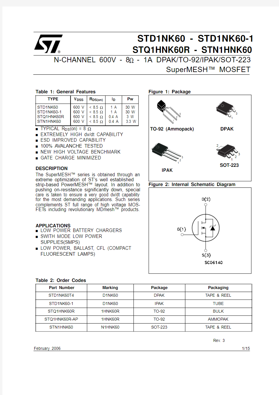
Table 1: General Features
■TYPICAL R DS (on) = 8 ?
■EXTREMELY HIGH dv/dt CAPABILITY ■ESD IMPROVED CAPABILITY ■100% AVALANCHE TESTED
■NEW HIGH VOLTAGE BENCHMARK ■
GATE CHARGE MINIMIZED
DESCRIPTION
The SuperMESH? series is obtained through an extreme optimization of ST’s well established strip-based PowerMESH? layout. In addition to pushing on-resistance significantly down, special care is taken to ensure a very good dv/dt capability for the most demanding applications. Such series complements ST full range of high voltage MOS-FET s including revolutionary MDmesh? products.APPLICATIONS
■LOW POWER BATTERY CHARGERS ■SWITH MODE LOW POWER SUPPLIES(SMPS)
■LOW POWER, BALLAST, CFL (COMPACT FLUORESCENT LAMPS)
Table 2: Order Codes
TYPE V DSS R DS(on)I D Pw STD1NK60STD1NK60-1STQ1HNK60R STN1HNK60
600 V 600 V 600 V 600 V
< 8.5 ?< 8.5 ?< 8.5 ?< 8.5 ?
1 A 1 A 0.4 A 0.4 A
30 W 30 W 3 W 3.3 W
2
1
TO-92 (Ammopack)Part Number Marking Package Packaging STD1NK60T4D1NK60DPAK TAPE & REEL
STD1NK60-1D1NK60IPAK TUBE STQ1HNK60R 1HNK60R TO-92BULK STQ1HNK60R-AP 1HNK60R TO-92AMMOPAK STN1HNK60
N1HNK60
SOT-223
TAPE & REEL
Rev. 3
STD1NK60 - STD1NK60-1 - STQ1HNK60R - STN1HNK60
2/15
Table 3: Absolute Maximum ratings
( ) Pulse width limited by safe operating area
(1) I SD ≤1.0A, di/dt ≤100A/μs, V DD ≤ V (BR)DSS , T j ≤ T JMAX.
Table 4: Thermal Data
(#) When mounted on FR-4 board of 1 in , 2oz Cu, t < 10 sec
Table 5: Avalanche Characteristics
ELECTRICAL CHARACTERISTICS (T CASE =25°C UNLESS OTHERWISE SPECIFIED)Table 6: On/Off
Symbol Parameter
Value
Unit DPAK / IPAK
TO-92
SOT-223
V DS Drain-source Voltage (V GS = 0)600V V DGR Drain-gate Voltage (R GS = 20 k ?)600V V GS Gate- source Voltage
± 30V
I D Drain Current (continuous) at T C = 25°C 1.00.40.4A I D Drain Current (continuous) at T C = 100°C 0.630.250.25A I DM ( )Drain Current (pulsed)4 1.6 1.6A P TOT Total Dissipation at T C = 25°C 303 3.3W Derating Factor
0.24
0.0250.025
W/°C dv/dt (1)Peak Diode Recovery voltage slope 3V/ns T j T stg
Operating Junction Temperature Storage Temperature
-55 to 150
°C
DPAK/IPAK
TO-92SOT-223
Unit Rthj-case Thermal Resistance Junction-case Max 4.16----°C/W Rthj-amb Thermal Resistance Junction-ambient Max 10012037.87 (#)
°C/W Rthj-lead
Thermal Resistance Junction-lead Max --40
--°C/W T l
Maximum Lead Temperature For Soldering Purpose
275
260
°C
Symbol Parameter
Max Value
Unit I AR Avalanche Current, Repetitive or Not-Repetitive (pulse width limited by T j max)
1A E AS
Single Pulse Avalanche Energy
(starting T j = 25 °C, I D = I AR , V DD = 50 V)
25
mJ
Symbol Parameter
Test Conditions
Min.Typ.
Max.
Unit V (BR)DSS Drain-source
Breakdown Voltage I D = 1mA, V GS = 0
600
V I DSS Zero Gate Voltage
Drain Current (V GS = 0)V DS = Max Rating
V DS = Max Rating, T C = 125 °C 150μA μA I GSS Gate-body Leakage Current (V DS = 0)V GS = ± 30V
±100nA V GS(th)Gate Threshold Voltage V DS = V GS , I D = 250 μA 2.25
3 3.7V R DS(on)
Static Drain-source On Resistance
V GS = 10V, I D = 0.5 A
8
8.5
?
3/15
STD1NK60 - STD1NK60-1 - STQ1HNK60R - STN1HNK60
ELECTRICAL CHARACTERISTICS (CONTINUED)Table 7: Dynamic
Table 8: Source Drain Diode
(1) Pulsed: Pulse duration = 300 μs, duty cycle 1.5 %.(2) Pulse width limited by safe operating area.
Symbol Parameter
Test Conditions
Min.
Typ.Max.
Unit g fs (1)Forward Transconductance V DS = 15 V , I D = 0.5 A 1S C iss C oss C rss Input Capacitance Output Capacitance
Reverse Transfer Capacitance V DS = 25V, f = 1 MHz, V GS = 0
15623.53.8pF pF pF t d(on)t r t d(off)t r Turn-on Delay Time Rise Time
Turn-off Delay Time Fall Time
V DD = 300 V, I D = 0.5 A,R G = 4.7 ?, V GS = 10 V
(Resistive Load see, Figure 21)
6.551925ns ns ns ns Q g Q gs Q gd
Total Gate Charge Gate-Source Charge Gate-Drain Charge
V DD = 480V, I D = 1 A,V GS = 10V, R G = 4.7 ?(see, Figure 23)
71.13.7
10nC nC nC
Symbol Parameter
Test Conditions
Min.
Typ.
Max.Unit I SD I SDM (2)Source-drain Current
Source-drain Current (pulsed)14A A V SD (1)Forward On Voltage I SD = 1.0 A, V GS = 0 1.6
V t rr Q rr I RRM Reverse Recovery Time Reverse Recovery Charge Reverse Recovery Current I SD = 1.0 A, di/dt = 100 A/μs V DD = 25V, T j = 25°C
(see test circuit, Figure 22)1402403.3ns μC A t rr Q rr I RRM
Reverse Recovery Time Reverse Recovery Charge Reverse Recovery Current
I SD = 1.0 A, di/dt = 100 A/μs V DD = 25V, T j = 150°C (see test circuit, Figure 22)
2293773.3
ns μC A
STD1NK60 - STD1NK60-1 - STQ1HNK60R - STN1HNK60
4/15
Figure 3: .Safe Operating Area For SOT-223
Figure 6: Thermal Impedance For SOT-223
5/15
STD1NK60 - STD1NK60-1 - STQ1HNK60R - STN1HNK60
Figure 9: Output Characteristics
Figure 12: Transfer Characteristics
STD1NK60 - STD1NK60-1 - STQ1HNK60R - STN1HNK60
6/15
Figure 15: Normalized Gate Thereshold Volt-
tics
Figure 18: Normalized On Resistance vs Tem-
DSS
STD1NK60 - STD1NK60-1 - STQ1HNK60R - STN1HNK60
Figure 21: Switching Times Test Circuit For Resistive Load
Figure 22: Test Circuit For Inductive Load Switching and Diode Recovery Times Figure 23: Gate Charge Test Circuit
7/15
STD1NK60 - STD1NK60-1 - STQ1HNK60R - STN1HNK60
8/15
STD1NK60 - STD1NK60-1 - STQ1HNK60R - STN1HNK60
9/15
STD1NK60 - STD1NK60-1 - STQ1HNK60R - STN1HNK60
10/15
STD1NK60 - STD1NK60-1 - STQ1HNK60R - STN1HNK60
11/15
STD1NK60 - STD1NK60-1 - STQ1HNK60R - STN1HNK60
12/15
13/15
STD1NK60 - STD1NK60-1 - STQ1HNK60R - STN1HNK60
TAPE AND REEL SHIPMENT
DPAK FOOTPRINT
DIM.mm inch MIN.
MAX.MIN.
MAX.A 330
12.992
B 1.50.059
C 12.813.20.5040.520
D 20.20.795G 16.418.40.6450.724N 50
1.968
T
22.40.881
BASE QTY BULK QTY 2500
2500REEL MECHANICAL DATA
DIM.mm inch MIN.MAX.MIN.
MAX.
A0 6.87
0.2670.275B010.410.60.4090.417
B112.10.476
D 1.5 1.60.0590.063D1 1.50.059
E 1.65 1.850.0650.073
F 7.47.60.2910.299K0 2.55 2.750.1000.108P0 3.9 4.10.1530.161P17.98.10.3110.319P2 1.9 2.1
0.0750.082R
40
1.574
W
15.7
16.3
0.618
0.641
TAPE MECHANICAL DATA
All dimensions are in millimeters
STD1NK60 - STD1NK60-1 - STQ1HNK60R - STN1HNK60
Table 9: Revision History
Date Revision Description of Changes 22-Nov-20042Added SOT-223 Package and new stylesheet
14-Feb-20063Modified marking on Table 2
14/15
STD1NK60 - STD1NK60-1 - STQ1HNK60R - STN1HNK60 Information furnished is believed to be accurate and reliable. However, STMicroelectronics assumes no responsibility for the consequences of use of such information nor for any infringement of patents or other rights of third parties which may result from its use. No license is granted
by implication or otherwise under any patent or patent rights of STMicroelectronics. Specifications mentioned in this publication are subject to change without notice. This publication supersedes and replaces all information previously supplied. STMicroelectronics products are not
authorized for use as critical components in life support devices or systems without express written approval of STMicroelectronics.
The ST logo is a registered trademark of STMicroelectronics
All other names are the property of their respective owners
? 2006 STMicroelectronics - All Rights Reserved
STMicroelectronics group of companies
Australia - Belgium - Brazil - Canada - China - Czech Republic - Finland - France - Germany - Hong Kong - India - Israel - Italy - Japan - Malaysia - Malta - Morocco - Singapore - Spain - Sweden - Switzerland - United Kingdom - United States of America
https://www.360docs.net/doc/618387463.html,
15/15
This datasheet has been downloaded from:
https://www.360docs.net/doc/618387463.html,
Free Download
Daily Updated Database
100% Free Datasheet Search Site
100% Free IC Replacement Search Site
Convenient Electronic Dictionary
Fast Search System
https://www.360docs.net/doc/618387463.html,
All Datasheets Cannot Be Modified Without Permission
Copyright ? Each Manufacturing Company