DTS6420规格书(最新版)

N-Channel 60-V (D-S) MOSFET
FEATURES
?Halogen-free According to IEC 61249-2-21Available
?TrenchFET ? Power MOSFET ?100 % R g Tested ?100 % UIS Tested
APPLICATIONS
?Battery Switch ?DC/DC Converter
PRODUCT SUMMARY
V DS (V)R DS(on) (Ω)I D (A)a
Q g (Typ.)60
0.078 at V GS = 10 V 3.4 2.1 nC
0.089 at V GS = 4.5 V
3.1
Notes:
a.Based on T C = 25 °C.
b.Surface Mounted on 1" x 1" FR4 board.
c.t = 5 s.
d.Maximum under Steady State conditions is 120 °C/W.
ABSOLUTE MAXIMUM RATINGS T A = 25 °C, unless otherwise noted
Parameter
Symbol Limit Unit Drain-Source Voltage V DS 60V
Gate-Source Voltage
V GS
± 20Continuous Drain Current (T J = 150 °C)T C = 25 °C I D 3.4A
T C = 70 °C 1.9T A = 25 °C 3.1b, c T A = 70 °C
1.8b, c Pulsed Drain Current
I DM 7Continuous Source-Drain Diode Current T C = 25 °C I S 1.49T A = 25 °C 0.91b, c
Avalanche Current
L = 0.1 mH I AS 6Single-Pulse Avalanche Energy E AS 1.8mJ Maximum Power Dissipation
T C = 25 °C P D 1.66W T C = 70 °C 1.06T A = 25 °C 1.09b, c T A = 70 °C 0.7b, c Operating Junction and Storage T emperature Range
T J , T stg
- 55 to 150
°C
THERMAL RESISTANCE RATINGS
Parameter Symbol
Typical Maximum Unit Maximum Junction-to-Ambient b, d
≤ 5 s R thJA 90115°C/W
Maximum Junction-to-Foot (Drain)Steady State R thJF 60
75
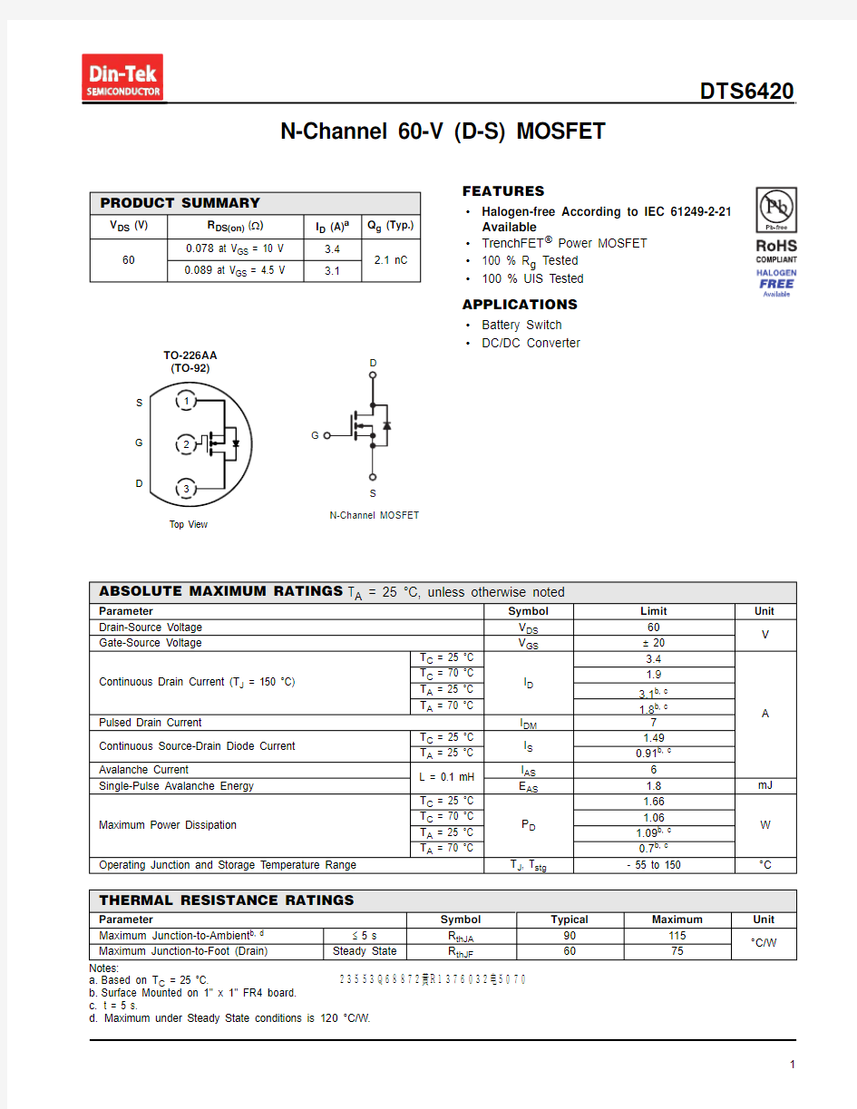
TO-226AA Top View
S
D
G
23553Q68872黄R1376032电5070
Notes:
a.Pulse test; pulse width ≤ 300 μs, duty cycle ≤ 2 %.
b.Guaranteed by design, not subject to production testing.
Stresses beyond those listed under “Absolute Maximum Ratings” may cause permanent damage to the device. These are stress ratings only, and functional operation of the device at these or any other conditions beyond those indicated in the operational sections of the specifications is not implied. Exposure to absolute maximum rating conditions for extended periods may affect device reliability.
MOSFET SPECIFICATIONS T J = 25 °C, unless otherwise noted
Parameter Symbol Test Conditions
Min.Typ.Max.Unit
Static
Drain-Source Breakdown Voltage V DS V DS = 0 V , I D = 250 μA
60
V V DS Temperature Coefficient ΔV DS /T J I D = 250 μA 55mV/°C V GS(th) T emperature Coefficient ΔV GS(th)/T J - 5
Gate-Source Threshold Voltage V GS(th) V DS = V GS , I D = 250 μA 13V Gate-Source Leakage
I GSS V DS = 0 V, V GS = ± 20 V ± 100nA Zero Gate Voltage Drain Current I DSS V DS = 60 V , V GS = 0 V 1μA V DS = 60 V, V GS = 0 V , T J = 55 °C
10
On-State Drain Current a
I D(on)V DS ≥ 5 V, V GS = 10 V 8
A Drain-Source On-State Resistance a R DS(on)V GS = 10 V , I D = 1.9 A 0.0750.078ΩV GS = 4.5 V , I D = 1.7 A 0.0860.089
Forward T ransconductance a g fs
V DS = 15V , I D = 1.9 A
5
S
Dynamic b
Input Capacitance C iss V DS = 30 V , V GS = 0 V , f = 1 MHz 180pF
Output Capacitance
C oss 22Reverse Transfer Capacitance C rss 13Total Gate Charge Q g V DS = 30 V , V GS = 10 V , I
D = 1.9 A 4.2 6.1nC V DS = 30 V, V GS = 4.5 V, I D = 1.9 A
2.1
3.2
Gate-Source Charge Q gs 0.7Gate-Drain Charge Q gd 1Gate Resistance R g f = 1 MHz
0.6
2.2 5.1Ω
Turn-On Delay Time t d(on) V DD = 30 V, R L = 20 Ω
I D ? 1.5 A, V GEN = 10 V , R G = 1 Ω
46ns Rise Time
t r 1015Turn-Off Delay Time t d(off) 1015Fall Time
t f 710.5Turn-On Delay Time t d(on) V DD = 30 V, R L = 20 Ω
I D = 1.5 A, V GEN = 4.5 V , R G = 1 Ω1523ns Rise Time
t r 1624Turn-Off Delay Time t d(off) 1117Fall Time
t f
11
17
Drain-Source Body Diode Characteristics Continuous Source-Drain Diode Current I S T C = 25 °C
2.19A Pulse Diode Forward Current a I SM 7Body Diode Voltage
V SD I S = 1.5 A
0.8 1.2V Body Diode Reverse Recovery Time t rr I F = 1.5 A, dI/dt = 100 A/μs, T J = 25 °C
1523ns Body Diode Reverse Recovery Charge Q rr 1015
nC Reverse Recovery Fall Time t a 12ns
Reverse Recovery Rise Time
t b
3
Output Characteristics Transfer Characteristics
On-Resistance vs. Junction Temperature
Threshold Voltage Single Pulse Power
Safe Operating Area
TYPICAL CHARACTERISTICS 25°C, unless otherwise noted
*The power dissipation P D is based on T J(max.) = 150 °C, using junction-to-case thermal resistance, and is more useful in settling the upper dissipation limit for cases where additional heatsinking is used. It is used to determine the current rating, when this rating falls below the package limit.
Current Derating*
Power Derating, Junction-to-Case
Power Derating, Junction-to-Ambient
THERMAL RATINGS (T A = 25 °C, unless otherwise noted)
Normalized Thermal Transient Impedance, Junction-to-Ambient
Normalized Thermal Transient Impedance, Junction-to-Foot
Mechanical Dimensions
TO-92
Dimensions in Millimeters