2SB1260-Q-TN3-B中文资料
UNISONIC TECHNOLOGIES CO., LTD
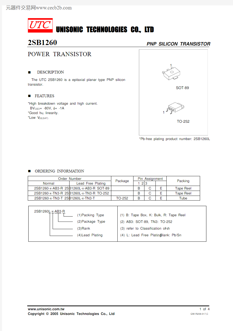
2SB1260
PNP SILICON TRANSISTOR
POWER TRANSISTOR
DESCRIPTION
The UTC 2SB1260 is a epitaxial planar type PNP silicon transistor.
FEATURES
*High breakdown voltage and high current. BV CEO = -80V, I C = -1A *Good h FE linearity. *Low V CE(SAT)
*Pb-free plating product number: 2SB1260L
ORDERING INFORMATION
Order Number Pin Assignment
Normal Lead Free Plating Package 1 2 3
Packing
2SB1260-x-AB3-R 2SB1260L-x-AB3-R SOT-89 B C E Tape Reel 2SB1260-x-TN3-R 2SB1260L-x-TN3-R TO-252 B C E Tape Reel 2SB1260-x-TN3-T 2SB1260L-x-TN3-T TO-252 B C E Tube
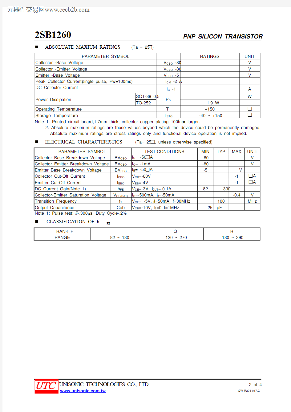
ABSOLUATE MAXIUM RATINGS (Ta = 25 )
PARAMETER SYMBOL RATINGS UNIT
Collector -Base Voltage V CBO -80 V Collector -Emitter Voltage V CEO -80 V Emitter -Base Voltage V EBO -5 V Peak Collector Current (single pulse, Pw=100ms) I CM -2 A DC Collector Current I C -1 A SOT-89 0.5 W
Power Dissipation
TO-252 P D
1.9 W
Operating Temperature T J +150
Storage Temperature
T STG -40 ~ +150
Note 1. Printed circuit board,1.7mm thick, collector copper plating 100mm 2 or larger.
2. Absolute maximum ratings are those values beyond which the device could be permanently damaged. Absolute maximum ratings are stress ratings only and functional device operation is not implied.
ELECTRICAL CHARACTERISTICS (Ta= 25 , unless otherwise specified)
PARAMETER SYMBOL
TEST CONDITIONS MIN TYP MAX UNIT Collector Base Breakdown Voltage BV CBO I C = -50 A -80 V Collector Emitter Breakdown Voltage BV CEO I C = -1mA -80 V
Emitter Base Breakdown Voltage BV EBO I E = -50 A
-5 V
Collector Cut-Off Current I CBO V CB =-60V -1 A Emitter Cut-Off Current I EBO V EB =-4V -1
A DC Current Gain(Note 1) h FE V CE =-3V, I OUT =-0.1A 82 390
Collector-Emitter Saturation Voltage V CE(SAT)I C =-500mA, I B =-50mA -0.4 V Transition Frequency f T V CE = -5V, I E =50mA, f=30MHz 100 MHz Output Capacitance Cob V CB =-10V, I E =0, f=1MHz 25 pF
Note 1: Pulse test: P W <300μs, Duty Cycle<2%
CLASSIFICATION OF h FE
RANK P Q R
RANGE 82 ~ 180 120 ~ 270 180 ~ 390
■
TYPICAL CHARACTERICS
Base to Emitter Voltage, V BE (V)
Grounded Emitter Propagation
Characteristics
C o l l e c t o r
C u r r e n t , I c (m
A )
Collector Current, Ic(mA)
DC Current Gain vs . Collector
D C C u r r e n t G a i n , h F E
Collector to Emitter Voltage, V CE (V)
Grounded Emitter Output
Characteristics
C o l l e c t o r C u r r e n t , I
c (m A )
Emitter Current , I E (mA)
Collector-emitter Saturation Voltage
C o l l e c t o r S a t u r a t i o n V o l t a g e , V C E (S A T ) ( V )
Collector to Base Voltage, V CB (V)
Collector Output Capacitance vs.
C o l l e c t o r O u t p u t C a p a c i t a n c e , C o b (p F )
Collector Current , Ic(mA)
T r a n s i t i o n F r e q u e n c y , f T (M H z )
Gain Bandwidth Product vs. Emitter
Current
TYPICAL CHARACTERICS(Cont.)
Collector to Emitter Voltage, V CE (V)
Safe Operating Area
C o l l e c t o r C u r r e n t , I c (A
)
Emitter To Base Voltage, V EB (V)Emitter Input Capacitance vs. Emitter-Base Voltage
E m i t t e r I n p u t C a p a c i t a n c e , C i b (p
F )