CS42888-DQZR中文资料

Copyright ? Cirrus Logic, Inc. 2006
(All Rights Reserved)
AUGUST '06
DS717F1
108 dB, 192 kHz 4-In, 8-Out CODEC
FEATURES
Four 24-bit A/D, Eight 24-bit D/A Converters ADC Dynamic Range
–105 dB Differential –102 dB Single-Ended DAC Dynamic Range
–108 dB Differential –105 dB Single-Ended ADC/DAC THD+N
–-98 dB Differential –
-95 dB Single-Ended
Compatible with Industry-Standard Time
Division Multiplexed (TDM) Serial Interface
System Sampling Rates up to 192 kHz Programmable ADC High-Pass Filter for DC
Offset Calibration
Logarithmic Digital Volume Control I2C ? & SPI ? Host Control Port
Supports Logic Levels Between 5V and 1.8V Popguard ? Technology GENERAL DESCRIPTION
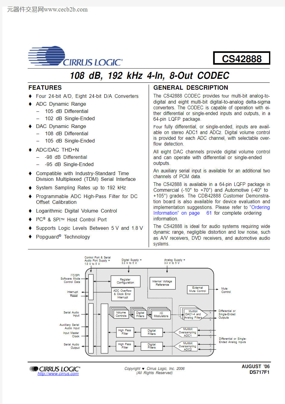
The CS42888 CODEC provides four multi-bit analog-to-digital and eight multi-bit digital-to-analog delta-sigma converters. The CODEC is capable of operation with ei-ther differential or single-ended inputs and outputs, in a 64-pin LQFP package.
Four fully differential, or single-ended, inputs are avail-able on stereo ADC1 and ADC 2. Digital volume control
is provided for each ADC channel, with selectable over-flow detection.
All eight DAC channels provide digital volume control and can operate with differential or single-ended outputs.
An auxiliary serial input is available for an additional two channels of PCM data.
The CS42888 is available in a 64-pin LQFP package in Commercial (-10° to +70°) and Automotive (-40° to +105°) grades. The CDB42888 Customer Demonstra-tion board is also available for device evaluation and implementation suggestions. Please refer to “Ordering Information” on page 61 for complete ordering information.
The CS42888 is ideal for audio systems requiring wide dynamic range, negligible distortion and low noise, such as A/V receivers, DVD receivers, and automotive audio systems.
CS42888
CS42888 TABLE OF CONTENTS
1. PIN DESCRIPTIONS (6)
1.1 Digital I/O Pin Characteristics (8)
2. TYPICAL CONNECTION DIAGRAM (9)
3. CHARACTERISTICS AND SPECIFICATIONS (10)
RECOMMENDED OPERATING CONDITIONS (10)
ABSOLUTE MAXIMUM RATINGS (10)
ANALOG INPUT CHARACTERISTICS (COMMERCIAL) (11)
ANALOG INPUT CHARACTERISTICS (AUTOMOTIVE) (12)
ADC DIGITAL FILTER CHARACTERISTICS (13)
ANALOG OUTPUT CHARACTERISTICS (COMMERCIAL) (14)
ANALOG OUTPUT CHARACTERISTICS (AUTOMOTIVE) (15)
COMBINED DAC INTERPOLATION & ON-CHIP ANALOG FILTER RESPONSE (17)
SWITCHING SPECIFICATIONS - ADC/DAC PORT (18)
SWITCHING CHARACTERISTICS - AUX PORT (20)
SWITCHING SPECIFICATIONS - CONTROL PORT - I2C MODE (21)
SWITCHING SPECIFICATIONS - CONTROL PORT - SPI FORMAT (22)
DC ELECTRICAL CHARACTERISTICS (23)
DIGITAL INTERFACE SPECIFICATIONS & CHARACTERISTICS (23)
4. APPLICATIONS (24)
4.1 Overview (24)
4.2 Analog Inputs (24)
4.2.1 Line-Level Inputs (24)
4.2.2 High-Pass Filter and DC Offset Calibration (25)
4.3 Analog Outputs (25)
4.3.1 Initialization (25)
4.3.2 Output Transient Control (27)
4.3.3 Popguard (27)
4.3.3.1 Power-Up (27)
4.3.3.2 Power-Down (27)
4.3.4 Mute Control (27)
4.3.5 Line-Level Outputs and Filtering (28)
4.3.6 Digital Volume Control (28)
4.3.7 De-Emphasis Filter (28)
4.4 System Clocking (29)
4.5 CODEC Digital Interface Formats (30)
4.5.1 I2S (31)
4.5.2 Left-Justified (31)
4.5.3 Right-Justified (31)
4.5.4 OLM #1 (31)
4.5.5 OLM #2 (32)
4.5.6 TDM (32)
4.5.7 I/O Channel Allocation (33)
4.6 AUX Port Digital Interface Formats (33)
4.6.1 I2S (33)
4.6.2 Left-Justified (33)
4.7 Control Port Description and Timing (33)
4.7.1 SPI Mode (34)
4.7.2 I2C Mode (34)
4.8 Interrupts (36)
4.9 Recommended Power-Up Sequence (36)
4.10 Reset and Power-Up (36)
4.11 Power Supply, Grounding, and PCB Layout (36)
CS42888
5. REGISTER QUICK REFERENCE (38)
6. REGISTER DESCRIPTION (40)
6.1 Memory Address Pointer (MAP) (40)
6.1.1 Increment (INCR) (40)
6.1.2 Memory Address Pointer (MAP[6:0]) (40)
6.2 Chip I.D. and Revision Register (Address 01h) (Read Only) (40)
6.2.1 Chip I.D. (CHIP_ID[3:0]) (40)
6.2.2 Chip Revision (REV_ID[3:0]) (40)
6.3 Power Control (Address 02h) (41)
6.3.1 Power Down ADC Pairs (PDN_ADCX) (41)
6.3.2 Power Down DAC Pairs (PDN_DACX) (41)
6.3.3 Power Down (PDN) (41)
6.4 Functional Mode (Address 03h) (42)
6.4.1 DAC Functional Mode (DAC_FM[1:0]) (42)
6.4.2 ADC Functional Mode (ADC_FM[1:0]) (42)
6.4.3 MCLK Frequency (MFREQ[2:0]) (42)
6.5 Interface Formats (Address 04h) (43)
6.5.1 Freeze Controls (FREEZE) (43)
6.5.2 Auxiliary Digital Interface Format (AUX_DIF) (43)
6.5.3 DAC Digital Interface Format (DAC_DIF[2:0]) (43)
6.5.4 ADC Digital Interface Format (ADC_DIF[2:0]) (44)
6.6 ADC Control & DAC De-Emphasis (Address 05h) (44)
6.6.1 ADC1-2 High-Pass Filter Freeze (ADC1-2_HPF FREEZE) (44)
6.6.2 DAC De-Emphasis Control (DAC_DEM) (45)
6.6.3 ADC1 Single-Ended Mode (ADC1 SINGLE) (45)
6.6.4 ADC2 Single-Ended Mode (ADC2 SINGLE) (45)
6.7 Transition Control (Address 06h) (45)
6.7.1 Single Volume Control (DAC_SNGVOL, ADC_SNGVOL) (45)
6.7.2 Soft Ramp and Zero Cross Control (ADC_SZC[1:0], DAC_SZC[1:0]) (46)
6.7.3 Auto-Mute (AMUTE) (46)
6.7.4 Mute ADC Serial Port (MUTE ADC_SP) (47)
6.8 DAC Channel Mute (Address 07h) (47)
6.8.1 Independent Channel Mute (AOUTX_MUTE) (47)
6.9 AOUTX Volume Control (Addresses 08h- 0Fh) (47)
6.9.1 Volume Control (AOUTX_VOL[7:0]) (47)
6.10 DAC Channel Invert (Address 10h) (48)
6.10.1 Invert Signal Polarity (INV_AOUTX) (48)
6.11 AINX Volume Control (Address 11h-14h) (48)
6.11.1 AINX Volume Control (AINX_VOL[7:0]) (48)
6.12 ADC Channel Invert (Address 17h) (48)
6.12.1 Invert Signal Polarity (INV_AINX) (49)
6.13 When enabled, these bits will invert the signal polarity of their respective channels.Status Control
(Address 18h) (49)
6.13.1 Interrupt Pin Control (INT[1:0]) (49)
6.14 Status (Address 19h) (Read Only) (49)
6.14.1 DAC CLOCK ERROR (DAC_CLK ERROR) (49)
6.14.2 ADC CLOCK ERROR (ADC_CLK ERROR) (50)
6.14.3 ADC Overflow (ADCX_OVFL) (50)
6.15 Status Mask (Address 1Ah) (50)
6.16 MUTEC Pin Control (Address 1Bh) (50)
6.17 MUTEC Polarity Select (MCPOLARITY) (50)
6.18 MUTE CONTROL ACTIVE (MUTEC ACTIVE) (50)
7. EXTERNAL FILTERS (51)
7.1 ADC Input Filter (51)
CS42888
7.1.1 Passive Input Filter (52)
7.1.2 Passive Input Filter w/Attenuation (52)
7.2 DAC Output Filter (53)
8. ADC FILTER PLOTS (54)
9. DAC FILTER PLOTS (56)
10. PARAMETER DEFINITIONS (58)
11. REFERENCES (59)
12. PACKAGE INFORMATION (60)
12.1 Thermal Characteristics (60)
13. ORDERING INFORMATION (61)
14. REVISION HISTORY (61)
LIST OF FIGURES
Figure 1.Typical Connection Diagram (9)
Figure 2.Output Test Circuit for Maximum Load (16)
Figure 3.Maximum Loading (16)
Figure 4.Serial Audio Interface Slave Mode Timing (18)
Figure 5.TDM Serial Audio Interface Timing (18)
Figure 6.Serial Audio Interface Master Mode Timing (19)
Figure 7.Serial Audio Interface Slave Mode Timing (20)
Figure 8.Control Port Timing - I2C Format (21)
Figure 9.Control Port Timing - SPI Format (22)
Figure 10.Full-Scale Input (25)
Figure 11.Audio Output Initialization Flow Chart (26)
Figure 12.Full-Scale Output (28)
Figure 13.De-Emphasis Curve (29)
Figure 14.I2S Format (31)
Figure 15.Left-Justified Format (31)
Figure 16.Right-Justified Format (31)
Figure 17.One-Line Mode #1 Format (31)
Figure 18.One-Line Mode #2 Format (32)
Figure 19.TDM Format (32)
Figure 20.AUX I2S Format (33)
Figure 21.AUX Left-Justified Format (33)
Figure 22.Control Port Timing in SPI Mode (34)
Figure 23.Control Port Timing, I2C Write (35)
Figure 24.Control Port Timing, I2C Read (35)
Figure 25.Single-to-Differential Active Input Filter (51)
Figure 26.Single-Ended Active Input Filter (51)
Figure 27.Passive Input Filter (52)
Figure 28.Passive Input Filter w/Attenuation (52)
Figure 29.Active Analog Output Filter (53)
Figure 30.Passive Analog Output Filter (53)
Figure 31.SSM Stopband Rejection (54)
Figure 32.SSM Transition Band (54)
Figure 33.SSM Transition Band (Detail) (54)
Figure 34.SSM Passband Ripple (54)
Figure 35.DSM Stopband Rejection (54)
Figure 36.DSM Transition Band (54)
Figure 37.DSM Transition Band (Detail) (55)
Figure 38.DSM Passband Ripple (55)
Figure 39.QSM Stopband Rejection (55)
Figure 40.QSM Transition Band (55)
CS42888 Figure 41.QSM Transition Band (Detail) (55)
Figure 42.QSM Passband Ripple (55)
Figure 43.SSM Stopband Rejection (56)
Figure 44.SSM Transition Band (56)
Figure 45.SSM Transition Band (detail) (56)
Figure 46.SSM Passband Ripple (56)
Figure 47.DSM Stopband Rejection (56)
Figure 48.DSM Transition Band (56)
Figure 49.DSM Transition Band (detail) (57)
Figure 50.DSM Passband Ripple (57)
Figure 51.QSM Stopband Rejection (57)
Figure 52.QSM Transition Band (57)
Figure 53.QSM Transition Band (detail) (57)
Figure 54.QSM Passband Ripple (57)
LIST OF TABLES
Table 1. I/O Power Rails (8)
Table 2. Single-Speed Mode Common Frequencies (29)
Table 3. Double-Speed Mode Common Frequencies (29)
Table 4. Quad-Speed Mode Common Frequencies (29)
Table 5. I2S, LJ, RJ Clock Ratios (30)
Table 6. OLM#1 Clock Ratios (30)
Table 7. OLM#2 Clock Ratios (30)
Table 8. TDM Clock Ratios (30)
Table 9. Serial Audio Interface Channel Allocations (33)
Table 10. MCLK Frequency Settings for I2S, Left and Right Justified Interface Formats (42)
Table 12. DAC Digital Interface Formats (43)
Table 11. MCLK Frequency Settings for TDM & OLM Interface Formats (43)
Table 13. ADC Digital Interface Formats (44)
Table 14. Example AOUT Volume Settings (47)
Table 15. Example AIN Volume Settings (48)
CS42888 1.PIN DESCRIPTIONS
Pin Name#Pin Description
AD0/CS1Address Bit [0]/ Chip Select (Input) - Chip address bit in I2C Mode. Control signal used to select the chip in SPI Mode.
AD1/CDIN2Address Bit [1]/ SPI Data Input (Input) - Chip address bit in I2C Mode. Input for SPI data.
RST3Reset (Input) - The device enters a low power mode and all internal registers are reset to their default settings when low.
VLC4Control Port Power (Input) - Determines the required signal level for the control port. See “Dig-ital I/O Pin Characteristics” on page8.
ADC_LRCK5ADC Left/Right Clock (Input/Output) - Determines which channel, Left or Right, is currently active on the ADC serial audio data line. Signals the start of a new TDM frame in the TDM digital interface format.
VD6, 24Digital Power (Input) - Positive terminal of the power supply for the digital section. DGND7, 23 62Digital Ground (Input) - Ground terminal of the power supply for the digital section.
VLS8Serial Port Interface Power (Input) - Determines the required signal level for the serial inter-faces. See “Digital I/O Pin Characteristics” on page8.
ADC_SCLK9ADC Serial Clock(Input/Output) - Serial clock for the ADC serial audio interface. Input fre-quency must be 256xFs in the TDM digital interface format.
MCLK10Master Clock (Input) - Clock source for the delta-sigma modulators and digital filters.
TSTO11Test Out - This pin is an output used for test purposes only. This pin must be not be connected to any external trace or other connection.
ADC_SDOUT1 ADC_SDOUT213
12
Serial Audio Data Output (Output) - Outputs for two’s complement serial audio data.
CS42888
DAC_SDIN1 DAC_SDIN2 DAC_SDIN3 DAC_SDIN417
16
15
14
DAC Serial Audio Data Input (Input) - Input for two’s complement serial audio data.
DAC_SCLK18DAC Serial Clock(Input/Output) - Serial clock for the DAC serial audio interface. Input fre-quency must be 256xFs in the TDM digital interface format.
DAC_LRCK19DAC Left/Right Clock (Input/Output) - Determines which channel, Left or Right, is currently active on the DAC serial audio data line. Signals the start of a new TDM frame in the TDM digital interface format.
AUX_LRCK20Auxiliary Left/Right Clock (Output) - Determines which channel, Left or Right, is currently active on the Auxiliary serial audio data line. Derived from the ADC serial port and equals Fs.
AUX_SCLK21Auxiliary Serial Clock(Output) - Serial clock for the Auxiliary serial audio interface.
AUX_SDIN22Auxiliary Serial Input (Input) - Provides an additional serial input for two’s complement serial audio data. Used only in the TDM digital interface format.
AOUT1 +,-AOUT2 +,-AOUT3 +,-AOUT4 +,-AOUT5 +,-AOUT6 +,-AOUT7 +,-AOUT8 +,-26, 25
27, 28
30, 29
31, 32
34, 33
36, 37
38, 39
40, 41
Differential Analog Output (Output) - The full-scale analog output level is specified in the Ana-log Characteristics table. Each leg of the differential outputs may also be used single-ended.
MUTEC35Mute Control (Output) - Used as a control for external mute circuits to prevent the clicks and pops that can occur in any single supply system.
AGND42, 56Analog Ground (Input) - Ground reference for the analog section.
VQ43Quiescent Voltage (Output) - Filter connection for internal quiescent reference voltage.
VA44, 53Analog Power (Input) - Positive power supply for the analog section. See “Digital I/O Pin Char-acteristics” on page8.
AIN1 +,-AIN2 +,-AIN3 +,-AIN4 +,-46, 45
48, 47
50, 49
52, 51
Differential Analog Input (Input) - Signals are presented differentially or single-ended to the Delta-Sigma modulators. The full-scale input level is specified in the Analog Characteristics specification table.
FILT+_DAC54Positive Voltage Reference (Output) - Positive reference voltage for the internal sampling cir-cuits of the DAC.
FILT+_ADC55Positive Voltage Reference (Output) - Positive reference voltage for the internal sampling cir-cuits of the ADC.
TSTN 57, 58
59, 60
Test In - This pin is an input used for test purposes only. It must be tied to ground for normal operation.
INT61Interrupt (Output) - Signals either an ADC overflow condition has occurred in one or more of the ADC inputs, or a clocking error has occurred in the DAC/ADC as specified in the Interrupt regis-ter.
SCL/CCLK63Serial Control Port Clock (Input) - Serial clock for the control port interface.
SDA/CDOUT64Serial Control Data I/O (Input/Output) - Input/Output for I2C data. Output for SPI data.
CS42888 1.1Digital I/O Pin Characteristics
Various pins on the CS42888 are powered from separate power supply rails. The logic level for each input should adhere to the corresponding power rail and should not exceed the maximum ratings.
Power
Rail
Pin Name I/O Driver Receiver VLC RST Input- 1.8 V - 5.0 V, CMOS SCL/CCLK Input- 1.8 V - 5.0 V, CMOS, with Hysteresis
SDA/CDOUT Input/
Output
1.8 V - 5.0 V, CMOS/Open Drain 1.8 V - 5.0 V, CMOS, with Hysteresis
AD0/CS Input- 1.8 V - 5.0 V, CMOS
AD1/CDIN Input- 1.8 V - 5.0 V, CMOS INT Output 1.8 V - 5.0 V, CMOS/Open Drain-
VLS MCLK Input- 1.8 V - 5.0 V, CMOS
ADC_LRCK Input/
Output
1.8 V - 5.0 V, CMOS 1.8 V - 5.0 V, CMOS
ADC_SCLK Input/
Output
1.8 V - 5.0 V, CMOS 1.8 V - 5.0 V, CMOS
ADC_SDOUT1-2Input/
Output
1.8 V - 5.0 V, CMOS-
DAC_LRCK Input/
Output
1.8 V - 5.0 V, CMOS 1.8 V - 5.0 V, CMOS
DAC_SCLK Input/
Output
1.8 V - 5.0 V, CMOS 1.8 V - 5.0 V, CMOS
DAC_SDIN1-4Input- 1.8 V - 5.0 V, CMOS AUX_LRCK Output 1.8 V - 5.0 V, CMOS-
AUX_SCLK Output 1.8 V - 5.0 V, CMOS-
AUX_SDIN Input- 1.8 V - 5.0 V, CMOS VA MUTEC Output 3.3 V - 5.0 V, CMOS-
Table 1. I/O Power Rails
CS42888 2. TYPICAL CONNECTION DIAGRAM
Figure 1. Typical Connection Diagram
CS42888
3.CHARACTERISTICS AND SPECIFICATIONS RECOMMENDED OPERATING CONDITIONS
(AGND=DGND=0 V, all voltages with respect to ground.)
ABSOLUTE MAXIMUM RATINGS
(AGND = DGND = 0 V; all voltages with respect to ground.)
WARNING:Operation at or beyond these limits may result in permanent damage to the device. Normal operation
is not guaranteed at these extremes.Notes:
1.Typical Analog input/output performance will slightly degrade at VA = 3.3 V.
2.The ADC_SDOUT may not meet timing requirements in TDM, Double-Speed Mode.
3.Any pin except supplies. Transient currents of up to ±100 mA on the analog input pins will not cause
SCR latch-up.4.The maximum over/under voltage is limited by the input current.
Parameters
Symbol Min Max Units DC Power Supply Analog (Note 1)VA
3.14 5.25V Digital
VD 3.14 5.25V Serial Audio Interface (Note 2)VLS 1.71 5.25V Control Port Interface VLC 1.71 5.25V Ambient Temperature
Commercial -CQZ Automotive -DQZ
T A
-10-40
+70+105
°C °C
Parameters
Symbol Min Max Units DC Power Supply
Analog Digital
Serial Port Interface Control Port Interface
VA VD VLS VLC -0.3-0.3-0.3-0.3 6.06.06.06.0V V V V Input Current
(Note 3)I in -±10mA Analog Input Voltage (Note 4)
V IN AGND-0.7VA+0.7V Digital Input Voltage Serial Port Interface (Note 4)
Control Port Interface
V IND-S V IND-C -0.3-0.3VLS+ 0.4VLC+ 0.4V V Ambient Operating Temperature (power applied)
T A -50
+125°C Storage Temperature
T stg
-65
+150
°C
CS42888 ANALOG INPUT CHARACTERISTICS (COMMERCIAL)
(Test Conditions (unless otherwise specified): T A=-10 to +70°C; VD = VLS = VLC = 3.3V±5%, VA = 5V±5%; Full-scale input sine wave: 1 kHz through the active input filter in Figure 25 on page 51 and Figure 26 on page 51; Measurement Bandwidth is 10Hz to 20kHz.)
Differential Single-Ended
Parameter Min Typ Max Min Typ Max Unit Fs=48 kHz, 96 kHz, 192 kHz
Dynamic Range A-weighted
unweighted
40 kHz bandwidth unweighted 99
96
-
105
102
99
-
-
-
96
93
102
99
96
-
-
-
dB
dB
dB
Total Harmonic Distortion + Noise -1dB (Note 5) -20dB
-60dB
40 kHz bandwidth -1 dB -
-
-
-
-98
-82
-42
-90
-92
-
-
-
-
-
-
-
-95
-79
-39
-90
-89
-
-
-
dB
dB
dB
dB
ADC1-2 Interchannel Isolation-90--90-dB DC Accuracy
Interchannel Gain Mismatch-0.1--0.1-dB Gain Drift-±100--±100-ppm/°C Analog Input
Full-Scale Input Voltage 1.06*VA 1.12*VA 1.18*VA0.53*VA0.56*VA0.59*VA Vpp Differential Input Impedance (Note 6)18-----k?Single-Ended Input Impedance (Note 7)---18--k?Common Mode Rejection Ratio (CMRR)-82----dB
CS42888 ANALOG INPUT CHARACTERISTICS (AUTOMOTIVE)
(Test Conditions (unless otherwise specified): T A=-40to+85°C; VD = VLS = VLC = 3.3V±5%, VA = 5V±5%; Full-scale input sine wave: 1 kHz through the active input filter in Figure 25 on page 51 and Figure 26 on page 51; Measurement Bandwidth is 10Hz to 20kHz.)
Notes:
5.Referred to the typical full-scale voltage.
6.Measured between AINx+ and AINx-.
7.Measured between AINxx and AGND.Differential Single-Ended
Parameter Min Typ Max Min Typ Max Unit Fs=48 kHz, 96 kHz, 192 kHz
Dynamic Range A-weighted
unweighted
40 kHz bandwidth unweighted 97
94
-
105
102
99
-
-
-
94
91
-
102
99
96
-
-
-
dB
dB
dB
Total Harmonic Distortion + Noise -1dB (Note 5) -20dB
-60dB
40 kHz bandwidth -1 dB -
-
-
-
-98
-82
-42
-87
-90
-
-
-
-
-
-
-
-95
-79
-39
-87
-87
-
-
-
dB
dB
dB
dB
ADC1-2 Interchannel Isolation-90--90-dB DC Accuracy
Interchannel Gain Mismatch-0.1--0.1-dB Gain Drift-±100--±100-ppm/°C Analog Input
Full-Scale Input Voltage 1.04*VA 1.12*VA 1.20*VA0.52*VA0.56*VA0.60*VA Vpp Differential Input Impedance(Note 6)18-----k?Single-Ended Input Impedance(Note 7)---18--k?Common Mode Rejection Ratio (CMRR)-82----dB
CS42888
ADC DIGITAL FILTER CHARACTERISTICS
Notes:
8.Filter response is guaranteed by design.
9.Response is clock-dependent and will scale with Fs. Note that the response plots (Figures 31to 42) have
been normalized to Fs and can be de-normalized by multiplying the X-axis scale by Fs.
Parameter (Notes 8, 9)
Min
Typ
Max
Unit
Single-Speed Mode (Note 9)Passband (Frequency Response) to -0.1 dB corner
0-0.4896Fs Passband Ripple --0.08dB Stopband
0.5688--Fs Stopband Attenuation 70--dB Total Group Delay
-12/Fs
-s
Double-Speed Mode (Note 9)Passband (Frequency Response) to -0.1 dB corner
0-0.4896Fs Passband Ripple --0.16dB Stopband
0.5604--Fs Stopband Attenuation 69--dB Total Group Delay
-9/Fs
-s
Quad-Speed Mode (Note 9)Passband (Frequency Response) to -0.1 dB corner
0-0.2604Fs Passband Ripple --0.16dB Stopband
0.5000--Fs Stopband Attenuation 60--dB Total Group Delay
-5/Fs
-s
High-Pass Filter Characteristics Frequency Response -3.0 dB -0.13 dB -120--Hz Hz Phase Deviation @ 20Hz
-10-Deg Passband Ripple --0dB Filter Settling Time -105/Fs
s
CS42888 ANALOG OUTPUT CHARACTERISTICS (COMMERCIAL)
(Test Conditions (unless otherwise specified): T A=-10to+70°C; VD = VLS = VLC = 3.3V±5%, VA = 5V±5%; Full-scale 997 Hz output sine wave (see Note 11) into passive filter in Figure 31 on page 54 and active filter in Fig-ure 31 on page 54; Measurement Bandwidth is 10Hz to 20kHz.)
Parameter
Differential
Min Typ Max
Single-Ended
Min Typ Max Unit
Fs = 48 kHz, 96 kHz, 192 kHz Dynamic Range
18 to 24-Bit A-weighted
unweighted 16-Bit A-weighted
unweighted 102
99
-
-
108
105
99
96
-
-
-
-
99
96
-
-
105
102
96
93
-
-
-
-
dB
dB
dB
dB
Total Harmonic Distortion + Noise
18 to 24-Bit0 dB
-20 dB
-60 dB 16-Bit0 dB
-20 dB
-60 dB -
-
-
-
-
-
-98
-85
-45
-93
-76
-36
-92
-
-
-
-
-
-
-
-
-
-
-95
-82
-42
-90
-73
-33
-89
-
-
-
-
-
dB
dB
dB
dB
dB
dB
Interchannel Isolation (1 kHz)-100--100-dB Analog Output
Full-Scale Output 1.235?VA 1.300?VA 1.365?VA0.618?VA0.650?VA0.683?VA Vpp Interchannel Gain Mismatch-0.10.25-0.10.25dB Gain Drift-±100--±100-ppm/°C Output Impedance-100--100-?DC Current draw from an AOUT pin
(Note 10)
--10--10μA AC-Load Resistance (R L)(Note 12)3--3--k?Load Capacitance (C L)(Note 12)--100--100pF
CS42888
ANALOG OUTPUT CHARACTERISTICS (AUTOMOTIVE)
(Test Conditions (unless otherwise specified): T A =-40 to +85°C; VD = VLS = VLC = 3.3V±5%, VA = 5V±5%; Full-scale 997 Hz output sine wave (see Note 11) in Figure 31 on page 54 and Figure 31 on page 54; Measure-ment Bandwidth is 10Hz to 20kHz.)
Notes:
10.Guaranteed by design. The DC current draw represents the allowed current draw from the AOUT pin
due to typical leakage through the electrolytic DC-blocking capacitors.11.One-half LSB of triangular PDF dither is added to data.
12.Guaranteed by design. See Figure 2. R L and C L reflect the recommended minimum resistance and
maximum capacitance required for the internal op-amp's stability and signal integrity. In this circuit to-pology, C L will effectively move the dominant pole of the two-pole amp in the output stage. Increasing this value beyond the recommended 100 pF can cause the internal op-amp to become unstable. See “External Filters” on page 51 for a recommended output filter.
Parameter
Differential
Min Typ Max
Single-Ended
Min Typ Max
Unit
Fs = 48 kHz, 96 kHz, 192 kHz Dynamic Range
18 to 24-Bit A-weighted
unweighted
16-Bit A-weighted
unweighted
10097--108
1059996----9794--1051029693----dB dB dB dB Total Harmonic Distortion + Noise
18 to 24-Bit 0 dB
-20 dB
-60 dB
16-Bit 0 dB
-20 dB
-60 dB
-------98-85-45-93-76-36-90------------95-82-42-90-73-33-87-----dB dB dB dB dB dB Interchannel Isolation (1 kHz)-100
-
-
100
-
dB
Analog Output Full-Scale Output 1.210?VA 1.300?VA 1.392?VA 0.605?VA 0.650?VA 0.696?VA Vpp Interchannel Gain Mismatch -0.10.25-0.10.25dB Gain Drift -±100--±100-ppm/°C Output Impedance -100--100-?DC Current draw from an AOUT pin (Note 10)--10--10μA
AC-Load Resistance (R L ) (Note 12)3--3--k ?Load Capacitance (C L )(Note 12)
-
-100
--100
pF
CS42888
Figure 2. Output Test Circuit for Maximum Load Figure 3. Maximum Loading
CS42888
COMBINED DAC INTERPOLATION & ON-CHIP ANALOG FILTER RESPONSE
Notes:
13.Response is clock-dependent and will scale with Fs. Note that the response plots (Figures 43to 54) have
been normalized to Fs and can be de-normalized by multiplying the X-axis scale by Fs.14.Single- and Double-Speed Mode Measurement Bandwidth is from Stopband to 3 Fs.
Quad-Speed Mode Measurement Bandwidth is from Stopband to 1.34 Fs.15.De-emphasis is only available in Single-Speed Mode.
Parameter (Notes 8, 13)
Min
Typ
Max
Unit
Single-Speed Mode
Passband (Frequency Response)to -0.05dB corner to -3dB corner
00--0.47800.4996Fs Fs Frequency Response 10Hz to 20kHz -0.2-+0.08dB StopBand
0.5465--Fs StopBand Attenuation (Note 14)
50--dB Group Delay
-10/Fs -s
De-emphasis Error (Note 15)
Fs = 32kHz Fs = 44.1 kHz Fs = 48 kHz
------+1.5/+0+0.05/-0.25-0.2/-0.4dB dB dB
Double-Speed Mode
Passband (Frequency Response)to -0.1dB corner to -3dB corner
00--0.46500.4982Fs Fs Frequency Response 10Hz to 20kHz -0.2-+0.7dB StopBand
0.5770--Fs StopBand Attenuation (Note 14)
55--dB Group Delay -5/Fs
-s
Quad-Speed Mode
Passband (Frequency Response)to -0.1dB corner to -3dB corner
00--0.3970.476Fs Fs Frequency Response 10Hz to 20kHz -0.2-+0.05dB StopBand
0.7--Fs StopBand Attenuation (Note 14)
51--dB Group Delay - 2.5/Fs
-s
CS42888
SWITCHING SPECIFICATIONS - ADC/DAC PORT
(Inputs: Logic 0 = DGND, Logic 1 = VLS, ADC_SDOUT C LOAD = 15 pF.)
Parameters (Note 20)
Symbol Min
Max
Units
Slave Mode
RST pin Low Pulse Width (Note 16)
1-ms MCLK Frequency 0.51250MHz MCLK Duty Cycle
(Note 17)
4555%Input Sample Rate (LRCK)
Single-Speed Mode
Double-Speed Mode (Note 18)Quad-Speed Mode (Note 19)
F s F s F s
45010050100200kHz kHz kHz LRCK Duty Cycle 4555%SCLK Duty Cycle 4555%
SCLK High Time t sckh
8-ns SCLK Low Time
t sckl 8-ns LRCK Rising Edge to SCLK Rising Edge
t fss t lcks 5-ns SCLK Rising Edge to LRCK Falling Edge
t fsh 16-ns SCLK Falling Edge to ADC_SDOUT Output Valid t dpd -35ns DAC_SDIN Setup Time Before SCLK Rising Edge t ds 3-ns DAC_SDIN Hold Time After SCLK Rising Edge t dh 5-ns DAC_SDIN Hold Time After SCLK Rising Edge t dh15-ns ADC_SDOUT Hold Time After SCLK Rising Edge t dh210-ns ADC_SDOUT Valid Before SCLK Rising Edge t dval
15-ns Master Mode
Output Sample Rate (LRCK) All Speed Modes F
s -MCLK / 256
kHz LRCK Duty Cycle 4555%SCLK Frequency -64 x Fs MHz SCLK Duty Cycle
4555%LRCK Edge to SCLK Rising Edge t lcks -5ns SCLK Falling Edge to ADC_SDOUT Output Valid t dpd -35ns DAC_SDIN Setup Time Before SCLK Rising Edge t ds 3-ns DAC_SDIN Hold Time After SCLK Rising Edge t dh1
5
-ns
Figure 5. TDM Serial Audio Interface Timing
CS42888 Notes:
16.After powering up the CS42888, RST should be held low after the power supplies and clocks are settled.
17.See Table10 on page42 and Table11 on page43 for suggested MCLK frequencies.
18.When operating in TDM interface format, VLS is limited to nominal 2.5 V to 5.0V operation only.
19.ADC - I2S, Left-Justified, Right-Justified interface formats only. DAC - I2S, Left-Justified, Right-Justified
and Time Division Multiplexed interface formats only.
20.“LRCK” and “SCLK” shall refer to the ADC and DAC left/right clock and serial clock, respectively.
Figure 6. Serial Audio Interface Master Mode Timing
CS42888 SWITCHING CHARACTERISTICS - AUX PORT
(Inputs: Logic 0 = DGND, Logic 1 = VLS.)
Parameters Symbol Min Max Units Master Mode
Output Sample Rate (AUX_LRCK) All Speed Modes F s-ADC_LRCK kHz AUX_SCLK Frequency-64·ADC_LRCK kHz AUX_SCLK Duty Cycle4555% AUX_LRCK Edge to SCLK Rising Edge t lcks-5ns AUX_SDIN Setup Time Before SCLK Rising Edge t ds3-ns
ns
AUX_SDIN Hold Time After SCLK Rising Edge t dh5-