A frequency and bandwidth tunable metamaterial absorber in x-band

A frequency and bandwidth tunable metamaterial absorber in x-band
H. Yuan, B. O. Zhu, and Y. Feng
Citation: Journal of Applied Physics 117, 173103 (2015); doi: 10.1063/1.4919753
View online: https://www.360docs.net/doc/7d16616873.html,/10.1063/1.4919753
View Table of Contents: https://www.360docs.net/doc/7d16616873.html,/content/aip/journal/jap/117/17?ver=pdfcov Published by the AIP Publishing
Articles you may be interested in
Triple-band low frequency ultra-compact metamaterial absorber
J. Appl. Phys. 117, 184503 (2015); 10.1063/1.4920994
Mechanically stretchable and tunable metamaterial absorber
Appl. Phys. Lett. 106, 091907 (2015); 10.1063/1.4914502
Bandwidth enhancement in disordered metamaterial absorbers
Appl. Phys. Lett. 105, 081102 (2014); 10.1063/1.4894181
Analysis of metamaterial absorber in normal and oblique incidence by using interference theory AIP Advances 3, 102118 (2013); 10.1063/1.4826522
Isotropic Mie resonance-based metamaterial perfect absorber
Appl. Phys. Lett. 103, 031910 (2013); 10.1063/1.4813914
A frequency and bandwidth tunable metamaterial absorber in x-band
H.Yuan,B.O.Zhu,a)and Y .Feng
School of Electronic Science and Engineering,Nanjing University,Nanjing 210023,China
(Received 16February 2015;accepted 23April 2015;published online 4May 2015)
Smart control is an attracting and important function for modern electromagnetic wave absorber.This paper presents the design,fabrication,and measurement of a frequency and bandwidth tunable metamaterial absorber (MA)in X-band.The unit cell of the MA consists of a microstrip resonator loaded with the varactors.Simulation and measurement results show that by tuning the bias voltage on the varactors,the peak absorption frequency can be tuned by 0.44GHz with the peak absorption greater than 95%.Field and circuit model analysis is conducted to reveal the work-ing mode and predict the absorbing frequency.After that,by specially designing the bias circuit so as to adjust the bias voltage on neighboring unit cells separately,dual resonance and absorption peaks occur,and the overall absorption bandwidth can thus be tuned conveniently by controlling the difference of the two resonance frequencies.The center absorbing frequency can also be tuned.Simulation and experiment results show that the 75%absorption (à6dB re?ection)bandwidth can be tuned from 0.40GHz to 0.74GHz,which is a two-fold tuning range.This work is believed to
improve the state-of-the-art smart metamaterial absorber.V
C 2015AIP Publishing LLC .[https://www.360docs.net/doc/7d16616873.html,/10.1063/1.4919753]
I.INTRODUCTION
Electromagnetic (EM)wave absorber is a functional ma-terial that absorbs the incident EM energy.Conventional EM absorbers are mainly realized by using materials with high electric loss,e.g.,the Salisbury screen,pyramid shaped foam impregnated with the mixture of carbon and iron,or by using materials with high magnetic polarization loss,e.g.,ferrite tile absorber.1–4
The metamaterial absorber (MA)is another new type of EM absorber proposed recently.5It is normally composed of electrically small unit cells arranged periodically in a two dimensional plane.Each unit cell can be regarded as the res-onant circuit.At resonance,MA exhibits purely effective surface resistance that is matched to the incident EM wave impedance for ef?cient wave absorption.The MA enjoys the features of light weight and low pro?le,but suffers from nar-row and ?xed absorbing frequency bandwidth.6–8
Since MA is realized through arti?cial design of the unit cell structure,one unique advantage of MA is that more functions than absorbing waves can be combined into MA,such as absorbing frequency tuning,9–12absorbing intensity tuning,13polarization independent absorbing,14–16multiple band absorbing,17–20wide incident angle absorber.21,22
Tunable absorbers are particularly useful components in wideband wireless communications systems,including the emerging system of cognitive radio networks and the intelli-gent radar system.During the past years,the tunable absorb-ers reported in literature focus mainly on the frequency tuning.However,bandwidth is also an important factor to tune in applications.23
In this paper,a bandwidth tunable MA in X-band is pre-sented.First,we employ microstrip line resonator to design
an absorbing frequency tunable MA.This approach is advan-tageous in X-band MA design.Then,by independently tun-ing the resonant absorbing frequencies of the unit cells in adjacent columns so as to control the resonant frequency difference,the overall absorbing bandwidth of the proposed MA can be tuned dynamically.The resonant mode of the unit cell is analyzed.Simulation and measurement is carried out to characterize its performance.
II.THE X-BAND FREQENCY TUNABLE MA EMLOYING MICROSTRIP RESONATOR A.Unit cell structure
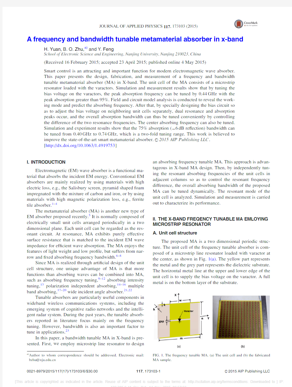
The proposed MA is a two dimensional periodic struc-ture.The unit cell of the frequency tunable absorber is com-posed of a microstrip line resonator loaded with varactor at the center,as shown in Fig.1(a).The yellow part represents the metal and the grey part represents the dielectric substrate.The horizontal metal line at the upper and lower edge of the unit cell is to supply the bias voltage on the varactor.A full metal is on the bottom layer of the
substrate.
FIG.1.The frequency tunable MA.(a)The unit cell and (b)the fabricated MA sample.
a)
Author to whom correspondence should be addressed.Electronic mail:bzhu@https://www.360docs.net/doc/7d16616873.html, 0021-8979/2015/117(17)/173103/6/$30.00V
C 2015AIP Publishing LLC 117,173103-1
JOURNAL OF APPLIED PHYSICS 117,173103
(2015)
Since the MA is a periodic structure,and the unit cell is symmetric with respect to both X and Y axes,the re?ection property for normal wave incidence can be studied by ana-lyzing the single unit cell enclosed by the perfect electric conductor(PEC)-perfect magnetic conductor(PMC)boun-dary condition.The PEC-PMC boundary condition actually constitutes a PEC-PMC waveguide which supports the plane wave as the fundamental mode with zero cut off frequency. The unit cell can be considered as the microstrip resonator loaded at the termination of the waveguide,and the wave-guide works as the feeding line for the resonator.When the unit cell resonates,it exhibits pure resistance to the feeding line,and its total input reactance is zero.By adjusting the size of the microstrip line and the thickness of the substrate, the resonance frequency can be designed.In order to achieve high absorption,the unit cell periodicity should be optimized in order to match the line impedance of the PEC-PMC wave-guide to the circuit impedance of the unit cell.Through tun-ing the bias voltage on the varactor at microstrip resonator center,the junction capacitance of the varactor is changed so that the resonance frequency,i.e.,the absorbing frequency, can be shifted.
B.Working mechanism
Fig.2illustrates the working mechanism.The unit cell can be regarded as two segments of microstrip line with short circuit termination due to the PEC boundary condition.The two segments are coupled through the varactor.Under the excitation of the fundamental mode of the PEC-PMC wave-guide,i.e.,plane wave excitation,the two segments of micro-strip line resonate out of phase,as shown in the Fig.2.Hence, the z component of the electric?eld is zero at YZ plane,so that there is a virtual PEC at that plane.As a result,each seg-ment can be modeled as the resonant circuit illustrated in Fig.
2.At lower frequencies,the varactor is an ordinary variable capacitor as shown in Fig.2(a).In the X-band,the varactor’s parasitic inductance dominates so that the varactor shall be regarded as a tunable inductor as shown in Fig.2(b).On the other hand,short-terminated microstrip line exhibits capaci-tance(inductance)to the varactor when it is longer(shorter) than its quarter guided operation wavelength,Hence,the pro-posed absorber can resonate at both higher and lower frequen-cies.When C varactor?0.9pF,simulation result shows that the ?rst resonance mode is at
3.16GHz,and the second one at 8.58GHz.Fig.2compares the electric?eld distribution of these two modes.As can be seen from the amplitude pro?le of the electric?eld distribution,the microstrip line in the half unit cell is shorter than quarter wavelength at3.16GHz,and longer than quarter wavelength at8.58GHz.The second reso-nant mode is important for high frequency MA design because it allows the moderate size of the unit cell rather than the one too small to be fabricated at high frequencies.
The current distribution on the top and ground metal also demonstrates the difference of the two working modes.A cur-rent strength null is observed near the unit cell center in the second resonant mode shown in Fig.2(b),while such a mini-mum point does not exist in the?rst mode shown in Fig.2(a), verifying that the microstrip line is shorter or longer than the quarter wavelength in the?rst or second mode,respectively. The current directions on the varactor are also different in these two modes relative to the current on the strip,due to the electric length variation of the microstrip resonator.
The resonant and absorbing frequency is predicted by using a little more accurate circuit model including the fringe inductance and capacitance at the gap discontinuity of the microstrip line where the varactor is soldered,as shown in Fig.3(a).The microstrip line exhibits capacitive reactance in X-band,and the varactor has an inductive reactance.L repre-sents the fringe inductance,and C represents the fringe ca-pacitance on the gap.The model’s total impedance Z is calculated as
Z?Z striptiwLt
1
iwC
Z varactor
1
iwC
tZ varactor
(1)
where Z strip is the input impedance of the short-terminated microstrip line and Z varactor is the varactor’s impedance.The resonant absorbing frequency can be obtained by letting the reactance of the total impedance Z equal to0.L,and C are determined by using the simulated resonant frequencies under two different varactor capacitance.
In Figs.3(b)and3(c),we use Eq.(1)to calculate the reso-nant frequencies for various varactor capacitance C varactor or microstrip resonator length n.When C varactor or n is increased, the resonance absorbing frequency decreases monotonously. Good agreement between the calculated results and simulated ones is achieved,which validates Eq.(1).
C.Experiment and simulation results
To verify the performance of the proposed tunable MA, we designed,fabricated,and measured a sample MA board. The metal is copper with the electric conductivity 5.8?107S/m.The optimized geometry dimensions of the unit cell are:m?16mm,n?10mm,w?8mm,h?0.8mm, gap?0.4mm,and k?0.2mm.The thickness of the copper ?lm is0.017mm.The dielectric substrate is FR4with the rel-ative permittivity4.1and loss tangent0.025.The varactor was modeled as the resistor,inductor,and capacitor in series in EM simulation.The varactor capacitance range is from 2.350pF at0V to0.466pF at15V.The varactor parasitic re-sistance is2.5X,and the parasitic inductance is1.1nH.A 210?244mm2sample board consisting of20?14unit cells was fabricated using printing circuit board technology,as shown in Fig.1(b).The SMV1231–011varactor is used in the board.
The experiment was performed in the microwave anechoic chambers.A vector network analyzer(Agilent E8363C)and two horn antennas were used to transmit EM waves onto the sample board and receive the re?ected sig-nals as sketched in Fig.4(a).The distance of the antenna to the sample is around3m.The incident angle is5degree to the normal of the sample.Due to the metallic ground so that EM transmission is zero,we only measured the re?ection coef?cient S11of the sample.The energy absorption can be further calculated as1àj S11j2.
FIG.2.The equivalent circuit model,
the E-?eld distribution at XZ plane,
and the surface current distribution(a)
for the?rst resonance mode at
3.16GHz and(b)for the second reso-
nance mode at8.58GHz.
with different(b)varactor capacitances and(c)microstrip resonator lengths.
When we increase the DC bias voltage from 0.0V to 15.0V,the varactor capacitance becomes smaller,leading to the rise of the absorbing frequency,as shown in Fig.5(a).The maximum re?ection attenuation is above 12dB during the absorbing frequency tuning.When the DC bias voltage is 0.0V,the measured absorption is 98.3%at 8.48GHz with the full width at half magnitude (FWHM)of 5%.As increas-ing the bias voltage,the absorption peak shifts to higher fre-quencies continuously.At 15.0V,the frequency of the peak absorption is 8.92GHz with the absorption rate of 95.2%and the FWHM of 5%.The tuning range of the absorbing fre-quency is 0.44GHz.
The peak absorption rate changes slightly as the peak absorbing frequency varies because we optimized the unit cell for the best absorption rate only at one particular capaci-tance value.The dashed lines in Fig.5(a)show the simulated re?ection at 0.0V and 15.0V for comparison.They differ from the measurement results a little bit.This is mainly due to two reasons.First,the varactor parameters used in simula-tion are measured at the frequency far lower than the X-band,so that the parasitic impedance effect of the diode at high frequency such as X-band is not taken into account.Second,the varactor soldering position may also affect the resonance frequency.However,the agreements are good overall between the experimental results and the simulation ones.The intermediate cases are also simulated,as shown in Fig.5(b).The peak absorption frequency shifts as the bias voltage is adjusted.The smallest capacitance corresponds to the highest bias voltage,and vice versa.
III.THE BANDWIDTH TUNABLE META-ABSORBER A.Unit cell configuration
Based on the frequency tunable MA presented above,we propose a bandwidth tuning mechanism by controlling
the bias voltages on different unit cells separately such that the whole MA will have tunable dual resonances and the overall absorption bandwidth can thus be adjusted and broadened.In addition,the center absorbing frequency can still be tuned if the bias voltages are tuned together.
The unit cell of the bandwidth tunable absorber is shown in Fig.6(a).In this design,bias voltages on the two varactors in adjacent microstrip resonators shown in Fig.6(b)are tuned independently.To do so,a bias network layer is designed as shown in Fig.6(c)and fabricated below the ground plane.Via holes are drilled to electrically connect the metal strips on the top layer and the bias voltage circuit layer.They are insulated from the ground plane.Under normal incidence,there is vir-tual PEC plane penetrating the upper and lower edges of the unit cell,hence placing via holes there does not in?uence the working performance of the absorber.
B.Experiment and simulation results
The optimized geometric dimensions of the bandwidth tunable MA are as follows:a ?16mm,b ?20mm,L 1?6mm,w 1?4.7mm,w 2?0.4mm,w 3?0.2mm,w 4?5.3mm,h 1?h 2?0.8mm.r 1?0.2mm is the radius of the via hole,and r 2?0.4mm is the radius of the hole on the ground where the via penetrates.Copper and FR4dielectric materials were used as the metal and dielectric substrate parts.
The full wave EM simulation based on the ?nite integra-tion technique was performed at the design and optimization stage.The unit cell boundary condition was applied to analyze the single unit cell.The incident wave’s electric ?eld is per-pendicular to the microstrip line gap since the design is polar-ization sensitive.The simulated re?ections are depicted as the dashed curves in Fig.7.When the two varactors are 0.6pF equally in one unit cell,the MA has only one absorbing peak with the narrowest bandwidth.As the right varactor is tuned to 2.35pF (0V)and the left one to 0.466pF (15V),the absorbing peak splits and bandwidth becomes the widest.From the results,we clearly see the bandwidth changing with different varactor capacitance.For the 75%absorption rate (à6dB re?ection),the bandwidth changes from 0.43GHz (10.76–11.19GHz)to 0.72GHz (10.55–11.28GHz),nearly doubling the bandwidth.
When the bandwidth is the widest,it is clear enough to observe the two absorption peaks at 10.78GHz and 11.10GHz in Fig.7,respectively.Fig.8shows the current distribution at these two frequencies.At 10.78GHz,
most
FIG.4.Measurement setup for (a)the frequency tunable MA and (b)the bandwidth tunable
MA.
FIG.5.(a)Measured (solid)and simu-lated (dash),and (b)simulated absorp-tion of the tunable MA at different bias voltage or varactor capacitance for the normal incident EM waves.
currents are distributed in the right resonator with the varac-tor capacitance of 2.35pF.At 11.10GHz,currents are mainly distributed in the left one with the varactor capaci-tance of 0.466pF.
The fabricated bandwidth tunable MA is shown in Figs.6(e)and 6(f).The sample board is 210mm ?202mm,consist-ing of 10?12unit cells.The experiment was performed using the focusing lens antennas measurement system,which is shown in Fig.4(b).The sample was placed at the focus of the two lens antennas,and the free space Transmission-Re?ection-Line calibration was applied to move the reference
plane to the MA’s surface.Two ports S parameters were measured with this setup,but only S 11is meaningful.
The measured re?ection of the bandwidth tunable MA is exhibited in Fig.7.V 1and V 2are the DC bias voltage of the left and right resonators in the unit cell,respectively.Because the left resonator is identical to the right one,we only change the left bias voltage from 0V to 7.5V,and the right one from 15V to 7.5V.When V 1?0V and V 2?15V,the bandwidth of the 75%absorption rate is 0.74GHz (from 10.72GHz to 11.50GHz),which is the widest bandwidth.As V 1increases to 7.5V and V 2decreases to 7.5V,the band-width of the 75%absorption rate narrows to the smallest value 0.34GHz (from 11.03GHz to 11.43GHz).The varia-tion is about two folded.In the measurement,Time Gate Technique is used to reduce multiple interference so that the measured curves in Fig.7are smooth.
The simulated and measured results observed in Fig.7are summarized in Table I .The small difference is due to the para-sitic impedance effect of the diode at high frequency and the varactor soldering position.However,the agreements are good overall between the experiment results and the simulation ones.
IV.SUMMARY
A frequency tunable X-band MA employing microstrip resonator is presented.It works under the second order mode where the varactor behaves as a tunable inductor,and the short terminated microstrip line as a lumped capacitor.This mode allows tunable MA design in high frequency band such as X-band where the parasitic inductance of the varac-tor would dominate.It is shown that the peak absorption frequency can be adjusted by 0.44GHz with the peak absorp-tion greater than 95%.By designing the bias circuit so as to adjust the varactors’capacitance in adjacent columns inde-pendently,a dual resonances MA is achieved.The distance of the two resonance frequencies can be adjusted so that the absorbing bandwidth can be tuned.In addition,the
absorbing
FIG.7.The simulation (dashed)and the experimental (solid)results of the bandwidth tunable MA at different bias voltages for normal incident EM
waves.
FIG.8.The current distributions of the bandwidth tunable MA.(a)At 10.78GHz.(b)At 11.10GHz.
TABLE I.The simulation and experiment results of the 75%absorption bandwidth.
Simulation (GHz)
Experiment (GHz)Narrowest bandwidth 0.430.40The range
10.76–11.19
11.03–11.43
Widest bandwidth 0.730.74The range
10.55–11.28
10.72–11.45
FIG.6.The bandwidth tunable MA.(a)The perspective view.(b)The top view.(c)The bottom view.(d)The side view.(e)The top and (f)the bottom view of the fabricated bandwidth tunable MA board.
frequency tuning is maintained if the bias voltages on differ-ent unit cells are tuned together.Simulation and experiment results show that the bandwidth of the75%absorption rate can be changed from0.40GHz to0.74GHz,which is two-fold https://www.360docs.net/doc/7d16616873.html,pared with the?rst order mode where the varactor exhibits the capacitive reactance,the second order mode is suitable for high frequency MA design where the varactors work as a tunable inductor and the microstrip line part provides the necessary capacitive reactance to meet the resonance condition.However,the frequency tuning range of the second order mode is generally smaller than that of the?rst order mode because of the dispersive effect of both the varactor impedance and microstrip line input impedance. Currently,the proposed design is polarization sensitive.It can be further developed to achieve polarization insensitive EM wave absorbing by using symmetric unit cell structure in the future.21,22Furthermore,the period of the proposed absorber is smaller than the half working wavelength so that the re?ected energy concentrates on the specular direction for oblique incidence.The tunable bandwidth MA can be used in some scienti?c and technological areas,particularly in electronically tunable spatial?lters.This work is believed to improve the state-of-art research of smart metamaterial absorber.
ACKNOWLEDGMENTS
This work was supported by the National Nature Science Foundation of China(Nos.61301017,61371034,60990322, and61101011),and the Key Grant Project of MoE of China (No.313029),and partially supported by the Priority Academic Program Development of Jiangsu Higher Education Institutions(PAPD)and Jiangsu Provincial Key Laboratory of Advanced Manipulating Technique of Electromagnetic Wave.
1E.F.Knott,J.F.Shaeffer,and M.T.Tuley,Radar Cross Section(Artech House,Norwood,1985).
2B. A.Munk,Frequency Selective Surface(John Willey&Sons, New York,2000).
3W.W.Salisbury,U.S.patent No.2,599,944(10June1952).
4S.M.Zhong and S.L.He,Sci.Rep.3,2083(2013).
https://www.360docs.net/doc/7d16616873.html,ndy,S.Sajuyigbe,J.J.Mock,D.R.Smith,and W.J.Padilla,Phys. Rev.Lett.100,207402(2008).
6H.Tao,https://www.360docs.net/doc/7d16616873.html,ndy,C.M.Bingham,X.Zhang,R.D.Averitt,and W.J. Padilla,Opt.Express16,7181(2008).
7W.J.Padilla,M.T.Aronsson,C.Highstrete,M.Lee,A.J.Taylor,and R.
D.Averitt,Phys.Rev.B75,041102(2007).
8M.Diem,T.Koschny,and C.M.Soukoulis,Phys.Rev.B79,033101 (2009).
9B.Zhu,Y.Feng,J.Zhao,C.Huang,and T.Jiang,Appl.Phys.Lett97, 051906(2010).
10J.Zhao,Q.Cheng,J.Chen,M.Q.Qi,W.X.Jiang,and T.J.Cui,New J. Phys.15,043049(2013).
11W.R.Xu and S.Sonkusale,Appl.Phys.Lett103,031902(2013).
12K.Aydin and E.Ozbay,J.Appl.Phys.101,024911(2007).
13X.Wu,C.Hu,Y.Wang,M.Pu,C.Huang,C.Wang,and X.Luo,AIP Adv.3,022114(2013).
14B.Zhu,Z.Wang,Z.Yu,Q.Zhang,J.Zhao,and Y.Feng,Chin.Phys.Lett. 26,114102(2009).
https://www.360docs.net/doc/7d16616873.html,ndy,C.M.Bingham,T.Tyler,N.Jokerst,D.R.Smith,and W.J. Padilla,Phys.Rev.B79,125104(2009).
16L.Li,Y.Yang,and C.H.Liang,J.Appl.Phys.110,063702(2011).
17S.Gu,J.P.Barrett,T.H.Hand,B.I.Popa,and S.A.Cummer,J.Appl. Phys.108,064913(2010).
18H.Tao, C.M.Bingham, D.Pilon,K. B.Fan, A. C.Strkwerda,D. Shrekenhamer,W.J.Padilla,X.Zhang,and R.D.Averitt,J.Phys.D: Appl.Phys.43,225102(2010).
19H.Li,L.H.Yuan,B.Zhou,X.P.Shen,Q.Cheng,and T.J.Cui,J.Appl. Phys.110,014909(2011).
20Y.Z.Cheng,Y.Wang,Y.Nie,R.Z.Gong,X.Xiong,and X.Wang, J.Appl.Phys.111,044902(2012).
21X.Y.Duan,S.Q.Chen,H.F.Yang,H.Cheng,J.J.Li,W.W.Liu,C.Z. Gu,and J.G.Tian,Appl.Phys.Lett.101,143105(2012).
22S.Q.Chen,H.Cheng,H.F.Yang,J.J.Li,X.Y.Duan,C.Z.Gu,and J.G. Tian,Appl.Phys.Lett.99,253104(2011).
23F.Bayatpur and K.Sarabandi,IEEE Trans.Microwave Theory Tech.57, 1433–1438(2009).
bandwidth 与 speed 区别
Cisco命令 bandwidth 与 speed 区别(转) 认识交换机带宽速度完成各种指令设置,交换机带宽速度是一个很重要的概念,如何深入了解就成了我们关注的问题,本文从指令设置认识速度与带宽,速度与带宽在交换机上的大不同两点深入讲解了交换机带宽速度。 对于网络使用者来说网络通讯速度与网络带宽是最重要的两个参数,速度speed直接决定了下载和上传数据的时间,从而直接影响页面浏览等网络访问效率;而带宽bandwidth则是企业网络使用情况的另外一个衡量标准,他是“频带宽度”的简称。从某种意义上讲带宽的多少也直接决定着网络的访问效率。实际上对于用户来说交换机带宽速度可以划一个等号,他们都是衡量网络传输效率的参数。但是你是否知道在交换机上速度与带宽所表达的不同意义呢?什么时候我们需要针对端口速度进行配置?什么时候对带宽的设置又更合适呢? 今天笔者就从自己的经验出发为各位读者介绍速度,交换机带宽bandwidth和速度speed在交换机上的大不同。 一、从指令设置认识速度与带宽: 有过配置路由交换经验的读者朋友都知道,在针对交换机进行配置时我们经常会用到两个参数,其中bandwith代表带宽,speed则代表速度。在实际配置时我们可以通过speed100将端口强制设置为100M速度,同时可以利用bandwidth2000将某端口设置限定交换机带宽速度为2M。 二、速度与带宽在交换机上的大不同: 正如上面所说我们可以针对端口的速度和带宽通过speed与bandwidth 分别配置,那么如果要将某端口速度强制设置为100M能够用 bandwidth100000呢?又或者说要将某端口交换机带宽速度限制为2M,是否也可以通过speed 2 指定其速度是2M呢?相信不少读者也和我一样存在上面的疑问,实际上通过笔者的多次测试发现不管我们通过命/令speed100还是bandwidth100000,最终该端口的传输速度都不会超过100M,相当于完成了限速的目的,两个命令起到的效果都是一样的。同理使用speed2还是bandwidth2000都是将带宽设置为2M,网络流量速度不会超过这个限定。既然两条命令都能够针对网络的速度进行设置,那么他们的功能是否相同呢?又或者说两者可以随意使用呢?答案是否定的,他们之间在一些功能上的体现是不同的,这也是为什么路由交换厂商会针对速度设置两个命令的原因。有些时候我们必须通过带宽bandwidth命令来设置端口速度,而另外一些情况要求我们利用speed命令来限定端口传输的速度。动态路由协议的应用:有经验的网管都知道路由协议在企业网络通讯过程中的重要意义,通过动态路由协议我们可以实现网络数据包的自动寻址,即使网络某条线路出现故障后也可以通过动态路由协议迅速找到另外一条新路来传输数据。 利用动态路由协议我们大大的简化了网络管理的工作量,而且在实际应用中的灵活性也随之提高。不过动态路由协议的"最佳"路径通常是通过某种
频数分布图的做法(函数法).
实例用数组公式: FREQUENCY 以一列垂直数组返回某个区域中数据的频率分布。例如,使用函数FREQUENCY 可以计算在给定的分数范围内测验分数的个数。由于函数FREQUENCY 返回一个数组,所以必须以数组公式的形式输入。 语法 FREQUENCY(data_array,bins_array) Data_array 为一数组或对一组数值的引用,用来计算频率。如果data_array 中不包含任何数值,函数FREQUENCY 返回零数组。(注:就是你想看分布的那些原始数据) Bins_array 为间隔的数组或对间隔的引用,该间隔用于对data_array 中的数值进行分组。如果bins_array 中不包含任何数值,函数FREQUENCY 返回data_array 中元素的个数。(注:就是你想用来分原始数据档的那些序列数,这个要自己根据需要先做好,备用) 说明 在选定相邻单元格区域(该区域用于显示返回的分布结果)后,函数FREQUENCY 应以数组公式的形式输入。 返回的数组中的元素个数比bins_array(数组)中的元素个数多1。返回的数组中所多出来的元素表示超出最高间隔的数值个数。例如,如果要计算输入到三个单元格中的三个数值区间(间隔),请一定在四个单元格中输入FREQUENCY 函数计算的结果。多出来的单元格将返回data_array 中大于第三个间隔值的数值个数。 函数FREQUENCY 将忽略空白单元格和文本。 对于返回结果为数组的公式,必须以数组公式的形式输入。 示例 本示例假设所有测验分数都为整数。 如果您将示例复制到空白工作表中,可能会更易于理解该示例。 操作方法 创建空白工作簿或工作表。 分数分段点 79 70 85 79 78 89 85 50 81 95 88 97 注:分数那一列拷贝到从A2-A10的部分,分段点列拷贝到B2-B5 公式说明(结果) =FREQUENCY(A2:A10,B2:B5) 分数小于等于70 的个数(1) 成绩介于71-79 之间的个数(2) 成绩介于80-89 之间的个数(4) 成绩大于等于90 的个数(2) 注释示例中的公式必须以数组公式的形式输入。将示例复制到空白工作表之后,请选中从公式单元格开始的单元格区域 A13:A16。按 F2,再按 Ctrl+Shift+Enter。如果公式未以数组公式的形式输入,则
关于测量控制与仪器仪表工程师资格认证若干问题的回答
关于测量控制与仪器仪表工程师资格认证 若干问题的回答 1、为什么要进行测量控制与仪器仪表工程师资格认证? 当今世界已进入信息时代,信息技术成为推动科学技术和国民经济发展的关键技术。测量控制与仪器仪表作为对物质世界的信息进行采集、处理、计量和控制的基础手段和设备,是信息产业的源头和重要组成部分。美国商务部国家技术和标准研究院(NIST)提出的报告称:美国90年代仪器仪表工业产值只占工业总产值的4%,但它对国民经济(GNP)的影响面却达到66%。仪器仪表是工业生产的"倍增器",科学研究的"先行官",军事上的"战斗力",国民活动中的"物化法官"。同时,仪器仪表在食品安全、商品质检、灾情预报、疾病控制、安全生产、反恐防毒等社会生活许多领域都有广泛应用,因此测量控制与仪器仪表在当今社会的重要作用怎样评估都不为过。 王现代测量控制与仪器仪表是机械、电子、计算机、材料、物理、化学、生物等领域先进技术的高度综合,是一个国家科技和国民经济发展水平的重要标志。测量控制与仪器仪表工程师是国家急需的专业技术人才,测量控制与仪器仪表工程师的水平是关系我国测量控制与仪器仪表事业发展的头等大事。测量控制与仪器仪表工程师资格认证就是以"公开、公平、公正"为原则,按与国际接轨的方式,对测量控制与仪器仪表专业技术人员的技术水平进行认证。这对我国测量控制与仪器仪表专业技术人员整体水平的提高、促进我国测量控制与仪器仪表的发展,进而加快和谐社会的建设及国民经济各行各业的快速发展具有深远的意义。 我国进入21世纪以来,测量控制与仪器仪表产业发展的平均年增长率超过国内经济发展的平均年增长率,达15%,测量控制与仪器仪表在国民经济各行各业和社会发展中的应用更是层出不穷;测量控制与仪器仪表的进口呈逐年上升之势,已成为我国进出口逆差最大的产业。这一发展趋势还将存在相当长一段时间,各行各业和社会发展急需高水平的测量控制和仪器仪表专业技术人员,测量控制和仪器仪表工程师资格认证对测量控制与仪器仪表有关用人单位量才录用及测量控制与仪器仪表专业技术人员的择业和人才流动将有较大的直接作用。 2、为什么要由中国仪器仪表学会开展测量控制与仪器仪表工程师资格认证工作?
外文翻译---我国仪器仪表与测量控制科技的发展
附录2:科技文献 我国仪器仪表与测量控制科技的发展 仪器仪表与测量控制在当今社会的重要地位和作用;我国仪器仪表与测量控制的基本概况;仪器仪表与测量控制发展的趋势和特点,以及我国仪器仪表与测量控制近年来的重大进展。 一地位作用 众所周知,当今世界已经进入信息时代,信息技术成为推动科学技术高速发展的关键技术。著名科学家钱学森明确指出,“信息技术包括测量技术、计算机技术和通信技术。测量技术是基础。”王大珩院士也一再强调,“测量技术是信息技术的源头。”信息技术的快速发展,产生了新兴的庞大的信息产业,信息产业已经成为带动世界经济发展的龙头产业。美国商业部1999年度报告在关于新兴数字经济部分提出,信息产业包括计算机软硬件行业、通信设备制造及服务行业、仪器仪表行业。这就是说,测量技术是信息技术的基础和源头,仪器仪表行业是信息产业的重要组成部分。不言而喻,仪器仪表与测量控制在当今信息时代推动科学技术和国民经济的发展具有何等重要的地位。 那么,仪器仪表与测量控制对推动科技、经济和社会的发展重要作用究竟是什么?2000年中国仪器仪表学会接受国家计委、国家经贸委和科技部的委托,组织了一个专家调研组对全国仪器仪表行业开展了一次为期3个月的调查研究。非常难得的是,王大珩、杨嘉墀、金国藩3位院士亲自参加了调研活动,并在调研结束后主持调研组向两委一部提出了一份“关于振兴我国仪器仪表产业对策与建议”的研究报告。这份报告对仪器仪表在当今社会的重要作用提出了明确而形象的说明,那就是我们都非常熟悉的:仪器仪表是工业生产的“倍增器”,科学研究的“先行官”,军事上的“战斗力”,以及现代社会活动的“物化法官”。这个说明的内涵和份量不需要再作任何解释,大家都一清二楚。令人鼓舞的是,仪器仪表与测量控制“倍增器”、“先行官”、“战斗力”和“物化法官”的重要作用已经为社会各界,包括政府部门所共识,成为加快发展仪器仪表科技和产业的科学依据,并在文件、报告和讲话中广为引用。 由于仪器仪表与测量控制的重要地位和作用受到了社会的高度重视,近些年来国家采取了一系列重大措施加快发展。值得特别提出的举措有:2001年3月举行的七届四次全国人大会议上提出“国家经济与社会发展第十个五年计划纲要”中明确提出“把发展仪器仪表放到重要位置”。国家发展纲要提到仪器仪表,而且放到重要位置,是建国以来的第一次。紧接着,国家计委、经贸委、科技部等许多部委都列了若干专项,动用了大笔资金支持仪器仪表的发展。2005年,国家发改委正式下
在Excel中使用FREQUENCY函数统计各分数段人数
在Excel中使用FREQUENCY函数统计各分数段人数 用Excel怎样统计出学生成绩各分数段内的人数分布呢?很多文章都推荐使用CountIF 函数,可是每统计一个分数段都要写一条函数,十分麻烦。例如,要在C58:C62内统计显示C2:C56内小于60分、60至70之间、70至80之间、80至90之间、90至100之间的分数段内人数分布情况,要输入以下5条公式: 1. 在C58内输入公式统计少于60分的人数:=CountIF(C2:C56,"<60") 2. 在C59内输入公式统计90分至100之间的人数:=CountIF(C2:C56,">=90") 3. 在C60内输入公式统计80至90之间的人数:=CountIF(C2:C56,">=80")-CountIF(C2:C56,">=90"), 4. 在C61内输入公式统计70到80之间的人数:=CountIF(C2:C56,">=70")-CountIF(C2:C56,">=80"), 5. 在C62内输入公式统计60到70之间的人数:=CountIF(C2:C56,">=60")-CountIF(C2:C56,">=70")。 如果要把0至10之间、10至20之间、20至30……90至100之间这么多个分数段都统计出来,就要写上十条公式了。可见用COUNTIF()函数效率并不高。 其实,Excel已经为我们提供了一个进行频度分析的FreQuency数组函数,它能让我们用一条数组公式就轻松地统计出各分数段的人数分布。 FREQUENCY函数说明如下: -------------------------------------------------- 语法: FREQUENCY(data_array,bins_array) 参数: data_array:需要进行频率统计的一组数。 bins_array:为间隔的数组,该间隔用于对data_array中的数值进行分组。 返回值: 以一列垂直数组返回某个区域中数据的频率分布。例如,使用函数FREQUENCY 可以计算在给定的分数范围内测验分数的个数。 注: 1、返回的数组中的元素个数比bins_array(数组)中的元素个数多1。所多出来的元素表示超出最高间隔的数值个数。 2、由于返回结果为数组,必须以数组公式的形式输入。即给定FREQUENCY的参数
低带宽 Low Bandwidth
低带宽Low Bandwidth 低存储Low Storage 低照度Low Illumination H.265超高清IP视频监控H.265 Super HD IP Video Surveillance 整体解决方案Integrated Solution 全球首发Global Premiere 5百万超高清5M Super HD ◆比H264节省带宽40% Less 40% Bandwidth than H.264 ◆自适应多帧WDR技术Adapt to Multiple Frames WDR Technology ◆增强ACM/DCI技术Enhance ACM/DCI Technology ◆40多种智能加速算子More than 40 kinds of Intelligent Acceleration Operator ◆<100ms 低延迟网传技术<100ms Low Latency Network Transmission Technology 超高清存储和显示Super HD Storage and Display ◆超强4核A17@1.6GHz Super 4 Nuclear: A17@1.6GHz ◆16路1080P H.265高清解码H.265 HD Decoding Technology: 16 channel 1080P ◆4K x 2K@60帧广电级显示Radio & Television Display: 4K x 2K@60 Frames ◆4K x 2K超高清转码Super HD Transcoding Technology: 4K x 2K ◆640Mbit/秒大带宽吞吐率Throughput Rate: 640Mbit/sec. Bandwidth
仪器仪表详细分类
照我国国民经济行业分类标准,仪器仪表大行业包括仪器仪表及计量器具等20 多个专业类别,即工业自动化仪表、电工仪器仪表、光学仪器、计时仪器、导航制导仪器、分析仪器、 试验机、实验室仪器、通用仪器仪表元器件、农林牧渔仪器仪表、地质地震仪器、气象海洋及水文天文仪器、核仪器、医疗仪器及设备、电子测量仪器、传递标准用计量仪器、衡器、船用仪表、汽车用仪表及其它通用仪器仪表等。按产品的主要服务对象和领域分,通常把仪器仪表大行业概括为生产过程测量控制仪表及系统、科学测试仪器、专用仪器仪表、仪表材料和元器件四大类。 我国仪器仪表行业的分布以机械系统开发生产通用仪器仪表为主,信息产业部、教育部、中国科学院、国家医药局和冶金、石化、轻工、煤炭、电力公司、测绘以及兵器、航天、航空、船舶工业等系统研制、生产各类专用仪器仪表;其中中科院(科学测试仪器)、信息产业部(通讯及电子测量仪器)、兵器、船舶及航空航天系统(军工配套产品)、轻工系统(衡器)、国家医药局(医疗仪器及设备)力量较强。 1、国际上仪器仪表是一个独立行业和产品领域,不属机械,也不属电子,内容还包括钟表行业。 2、按行业行政归口,我国长期将电影机械、照相机、复印机等文化办公设备行业也归入仪器仪表行业。 3、随着计算机的发展,各种测量控制装置中,计算机的应用日益广泛,特别是调节控制系统中的计算机及其软件涉及行业分类和政策优惠。 3577 衡器制造 指用来测定物质重量的各种机械的、电子的或机电结合的装置或设备的生产。包括: -固定式秤:轨道衡、汽车衡、地中衡等; -轻便或可移动式秤:台秤、案秤、吊秤、轴重秤、健康秤、家用秤、 便携秤等;
人力资源常用EXCEL函数汇总
1、利用身份证号码提取员工性别信息 我国新一代的18 位身份证号码有一个很明显的特征,身份证号的倒数第2 位是奇数,为男性,否则是女性。根据这一特征,利用MID 和TRUNC两个函数判断员工的性别,而不必逐个输入,这样既避免了输入的烦琐工作,又保证了数据的正确性 操作步骤: 在单元格区域E3:E19 中输入员工的身份证号码。 MID 返回文本字符串中从指定位置开始指定数目的字符,该数目由用户指定。格式:MID(text,start_num,num_chars)。参数:text(文本)代表要提取字符的文本字符串;start_num(开始数值)代表文本中要提取字符的位置,文本中第1 个字符的start_num 为1,以此类推;num_chars(字符个数)指定MID 从文本中返回字符的个数。
函数TRUNC 的功能是将数字的小数部分截去,返回整数。格式:TRUNC(number,num_digits)。参数:number(数值)需要截尾取整的数字。num_digits(阿拉伯数字)用于指定取整精度的数字,num_digits 的默认值为0。 2、利用身份证号码提取员工出生日期信息 利用身份证号码来提取员工的出生日期,既准确又节省时间。具体操作步骤如图
函数TEXT 功能是将数值转换为指定数字格式表示的文本。格式:TEXT(value,format_text)。参数:value(数值)指数值、计算结果为数字值的公式,或对包含数字值的单元格的引用;format_text(文本格式)为【单元格格式】对话框中【数字】选项卡上【分类】文本框中的文本形式 的数字格式。函数LEN 功能是返回文本字符串中的字符数。格式:LEN(text)。参数:text 表示要查找的文本,空格将作为字符进行计数。 3、计算员工年龄 企业中的职务变动和员工的年龄有密切的关系,员工年龄随着日期变化而变动,借助于函数YEAR 和TODAY 可以轻松输入。 选择单元格区域F3:F19,单击【开始】选项卡,在【数字】组中单击
测量控制与仪器仪表工程师资格培训教材大纲
测量控制与仪器仪表工程师资格培训教材大纲 《测量控制与仪器仪表现代系统集成技术》 1.绪论 1.1 仪器仪表在国民经济中的地位 1.2 仪器仪表技术的发展现状 1.3 现代仪器仪表系统的基本结构与组成 1.4 仪器仪表系统集成的基本概念及意义 思考题 2. 仪器仪表中的传感集成技术 2.1 现代传感技术的发展 2.2 现代传感技术在仪器仪表集成系统中的位置和作用 2.3 测量系统的基本功能 2.3.1 测量系统的功能模块组成 2.3.2 功能模块间的相互作用 2.4 传感器的分类 2.4.1 按被测量进行的分类 2.4.2 按作用原理进行的分类 2.4.3 按能量转换关系进行的分类 2.4.4 常用传感器的种类列表 2.5 典型传感器及其在仪器仪表系统集成中的应用 2.5.1 电阻式传感器及其应用 2.5.2 电感式传感器及其应用 2.5.3 涡流传感器及其应用 2.5.4 电容式传感器及其应用 2.5.5 压电传感器及其应用 2.5.6 磁电式传感器及其应用 2.6 光电传感技术 2.6.1 光电传感技术基础 2.6.2 光谱测试技术 2.6.3 莫尔条纹测量技术 2.6.4 干涉测量技术 2.6.5 光纤传感技术
2.7 微型传感集成系统 2.7.1 概述 2.7.2 微型传感器 2.7.3 微型传感集成系统应用 思考题 3. 系统及系统特性描述 3.1 系统集成概念 3.1.1 系统集成概念的提出和发展 3.1.2 系统集成的基本结构形式 3.2 基本集成模块 3.2.1 物理层配置 3.2.2 应用层 3.3 系统建模及仿真 3.3.1 系统需求分析 3.3.2 建模及仿真 3.4 系统控制 3.4.1 分散型控制系统(DCS) 3.4.2 现场总线控制系统(FCS) 3.4.3 可编程逻辑控制(PLC) 3.4.4 数字信号处理器(Digital Signal Processor ,简记为DSP) 3.4.5 嵌入式控制器 3.4.6PID控制器 3.4.7 最优控制 3.4.8 自适应控制 思考题 4. 仪器仪表计算机系统集成技术 4.1 计算机集成仪器仪表系统的基本功能结构 4.1.1 数据的融合与综合利用 4.1.2 网络体系结构与网络协议 4.1.3 Internet国际互联网 4.1.4 现场总线技术 4.2 系统集成中的计算机接口技术
FREQUENCY函数说明
FREQUENCY函数说明 计算数值在某个区域内的出现频率,然后返回一个垂直数组。例如,使用函数FREQUENCY 可以在分数区域内计算测验分数的个数。由于函数 FREQUENCY 返回一个数组,所以它必须以数组公式的形式输入。 语法 FREQUENCY(data_array,bins_array) Data_array 是一个数组或对一组数值的引用,您要为它计算频率。如果 data_array 中不包含任何数值,函数 FREQUENCY 将返回一个零数组。 Bins_array 是一个区间数组或对区间的引用,该区间用于对 data_array 中的数值进行分组。如果 bins_array 中不包含任何数值,函数 FREQUENCY 返回的值与 data_array 中的元素个数相等。 说明:在选择了用于显示返回的分布结果的相邻单元格区域后,函数 FREQUENCY 应以数组公式的形式输入。返回的数组中的元素个数比 bins_array 中的元素个数多 1 个。多出来的元素表示最高区间之上的数值个数。例如,如果要为三个单元格中输入的三个数值区间计数,请务必在四个单元格中输入 FREQUENCY 函数获得计算结果。多出来的单元格将返回 data_array 中第三个区间值以上的数值个数。 函数 FREQUENCY 将忽略空白单元格和文本。如果公式的返回结果为数组,该公式必须以数组公式的形式输入。本示例假设所有测验分数都是整数。 请选择从公式单元格开始的区域 A13:A16。按 F2,再按 Ctrl+Shift+Enter。如果公式未以数组公式的形式输入,则返回的结果为 1。 若分段数组无序,则分段情况不变,但显示规律是:假设分段数组为a\b\c\d\e\f\g。则A位置显示<=A的部分,B位置显示<=B的部分……依此类推,F位置显示<=F的部分,G位置显示<=G的部分,最后显示>最大数的部分。
各种带宽概念详解,适合初学者
?什么是带宽? ? 在各类电子设备和元器件中,我们都可以接触到带宽的概念,例如我们熟知的显示器的带宽,内存的带宽,总线的带宽和网络的带宽等等;对这些设备而言,带宽是一个 非常重要的指标.不过容易让人迷惑的是,在显示器中它的单位是MHz,这是一个频率 的概念;而在总线和内存中的单位则是GB/s,相当于数据传输率的概念;而在通讯领域, 带宽的描述单位又变成了MHz,GHz……这两种不同单位的带宽表达的是同一个内涵么 二者存在哪些方面的联系呢本文就带你走入精彩的带宽世界. 一, 带宽的两种概念 第一种如果从电子电路角度出发,带宽(Bandwidth)本意指的是电子电路中存在一个固有通频带,这个概念或许比较抽象,我们有必要作进一步解释.大家都知道,各类复杂 的电子电路无一例外都存在电感,电容或相当功能的储能元件,即使没有采用现成的电 感线圈或电容,导线自身就是一个电感,而导线与导线之间,导线与地之间便可以组成 电容——这就是通常所说的杂散电容或分布电容;不管是哪种类型的电容,电感,都会 对信号起着阻滞作用从而消耗信号能量,严重的话会影响信号品质.这种效应与交流电 信号的频率成正比关系,当频率高到一定程度,令信号难以保持稳定时,整个电子电路 自然就无法正常工作.为此,电子学上就提出了"带宽"的概念,它指的是电路可以保 持稳定工作的频率范围.而属于该体系的有显示器带宽,通讯/网络中的带宽等等. 而第二种带宽的概念大家也许会更熟悉,它所指的其实是数据传输率,譬如内存带宽,总线带宽,网络带宽等等,都是以"字节/秒"为单位.我们不清楚从什么时候起 这些数据传输率的概念被称为"带宽",但因业界与公众都接受了这种说法,代表数据 传输率的带宽概念非常流行,尽管它与电子电路中"带宽"的本意相差很远. 区别:对于电子电路中的带宽,决定因素在于电路设计.它主要是由高频放大部分元件的特性决定,而高频电路的设计是比较困难的部分,成本也比普通电路要高很多.这部分 内容涉及到电路设计的知识,对此我们就不做深入的分析.而对于总线,内存中的带宽, 决定其数值的主要因素在于工作频率和位宽,在这两个领域,带宽等于工作频率与位宽 的乘积,因此带宽和工作频率,位宽两个指标成正比.不过工作频率或位宽并不能无限制提高,它们受到很多因素的制约。 我们会在接下来的总线,内存部分对其作专门论述. 二, 总线中的带宽 在计算机系统中,总线的作用就好比是人体中的神经系统,它承担的是所有数据传输的职责,而各个子系统间都必须籍由总线才能通讯,例如,CPU和北桥间有前端总线, 北桥与显卡间为AGP总线,芯片组间有南北桥总线,各类扩展设备通过PCI,PCI-X总 线与系统连接;主机与外部设备的连接也是通过总线进行,如目前流行的USB 2.0, IEEE1394总线等等,一句话,在一部计算机系统内,所有数据交换的需求都必须通过总 线来实现! 按照工作模式不同,总线可分为两种类型,一种是并行总线,它在同一时刻可以传输多位数据,好比是一条允许多辆车并排开的宽敞道路,而且它还有双向单向之分;另 一种为串行总线,它在同一时刻只能传输一个数据,好比只容许一辆车行走的狭窄道路, 数据必须一个接一个传输,看起来仿佛一个长长的数据串,故称为"串行". 并行总线和串行总线的描述参数存在一定差别.对并行总线来说,描述的性能参数 有以下三个:总线宽度,时钟频率,数据传输频率.其中,总线宽度就是该总线可同时
测控技术与仪器专业调研报告
测控技术与仪器专业 调研报告 班级: 学生姓名: 学号: 题目:测控技术与仪器专业调研报告完成日期 2013年6月11日
前言 俄国化学家门捷列夫指出:“科学是从测量开始的”。英国物理学家开尔文勋爵(William Thomson)说过:“当你能测量并用数字来表达你所谈及的事物,你对它是有所了解的。反之,你的知识是贫瘠的和不能令人满意的,无论该事物是何种事物,你或许处于知识的启蒙阶段,但你尚还未进入科学的殿堂。因此,如果说科学是测量的话,那么,没有测量学(Metrology)便没有科学。”上述论断指出了测量在科学技术领域的极端重要性。此外,在产品的研究、开发、加工、制造和质量检验,在贸易、交通、环境保护以及医疗卫生等各个领域,都离不开测量[1]。 测控技术是一门研究信息的获取和处理,以及对相关要素进行控制的理论与技术;是电子、光学、精密机械、计算机、信息与控制技术多学科互相渗透而形成的一门高新技术密集型综合学科。一般是指对工业生产过程及其机电设备进行测量与控制的自动化技术,是计算机技术与自动控制技术结合的产物。测控技术主要研究如何将自动化系统上的信号加以采集、整理、处理、而后进行显示或者发出控制信号的过程并设计出所需要的计算机测控系统。测就是测量和感知,也就是要获得目标对象的信息,控就是控制,是根据目标对象的现象判断目标对象是否符合预期控制目标,并采取相应措施。测和控只是某一时间段就可以完成的行为,而根据测量结果判断目标状态是否符合要求则需要控制算法的判断参与,这一作出决定的过程可以由人工或控制系统来完成,测、控、以及控制算法就构成一个测控系统。 随着科学技术的不断发展,在工业生产领域中,测控技术得到了快速的进步,这是一项新兴的科学技术,是工业生产发展到一定阶段的必然产物。在现代化生产技术下,信息技术和计算机科学不断的融入到生产领域中,将这些技术不断的融合创新,对工业生产有了极大的推动力。现代测控技术以其超高的技术含量在工业生产领域中发挥着重要的作用,不断的将现代无线技术、定位技术应用到工业生产中,为工业生产的发展创造了有利的环境[2]。 一测控技术背景意义 测控装置的出现可以追溯到很早,早在公元前14世纪,我国就发明了漏壶计时器。在公元前427年,伟大的希腊哲学家柏拉图就已经提出了“控制论”一词。而真正的自动控制产生是在1788年,瓦特发明的蒸汽机中使用调速器(离心式飞轮)。然而,测控工程作为一门学科,它的形成并迅速发展只有五六十年的历史。因此,我们可以认为测控技术是刚发展起来的一门新兴学科。 测控技术发展至今大体经历了三个阶段:1、应用仪表自动监测生产过程中的数据;2、采用控制仪表或控制机构,代替人工操作;3、出现计算机控制系统,形成生产的全自动化。 二测控技术的特点 进入21世纪以来,随着现代社会市场经济快速的发展和水平的提高,现代科学技术的飞速发展和不断融入,有效地促进了测控技术的发展,使测控技术朝
关于测量控制与仪器仪表工程师资格认证若干问题的回答
关于测量控制与仪器仪表工程师资格认证若干 问题的回答 1、为什么要进行测量控制与仪器仪表工程师资格认证? 当今世界已进入信息时代,信息技术成为推动科学技术和国民经济发展的关键技术。测量控制与仪器仪表作为对物质世界的信息进行采集、处理、计量和控制的基础手段和设备,是信息产业的源头和重要组成部分。美国商务部国家技术和标准研究院(NIST)提出的报告称:美国90年代仪器仪表工业产值只占工业总产值的4%,但它对国民经济(GNP)的影响面却达到66%。仪器仪表是工业生产的"倍增器",科学研究的"先行官",军事上的"战斗力",国民活动中的"物化法官"。同时,仪器仪表在食品安全、商品质检、灾情预报、疾病控制、安全生产、反恐防毒等社会生活许多领域都有广泛应用,因此测量控制与仪器仪表在当今社会的重要作用怎样评估都不为过。 王现代测量控制与仪器仪表是机械、电子、计算机、材料、物理、化学、生物等领域先进技术的高度综合,是一个国家科技和国民经济发展水平的重要标志。测量控制与仪器仪表工程师是国家急需的专业技术人才,测量控制与仪器仪表工程师的水平是关系我国测量控制与仪器仪表事业发展的头等大事。测量控制与仪器仪表工程师资格认证就是以"公开、公平、公正"为原则,按与国际接轨的方式,对测量控制与仪器仪表专业技术人员的技术水平进行认证。这对我国测量控制与仪器仪表专业技术人员整体水平的提高、促进我国测量控制与仪器仪表的发展,进而加快和谐社会的建设及国民经济各行各业的快速发展具有深远的意义。 我国进入21世纪以来,测量控制与仪器仪表产业发展的平均年增长率超过国内经济发展的平均年增长率,达15%,测量控制与仪器仪表在国民经济各行各业和社会发展中的应用更是层出不穷;测量控制与仪器仪表的进口呈逐年上升之势,已成为我国进出口逆差最大的产业。这一发展趋势还将存在相当长一段时间,各行各业和社会发展急需高水平的测量控
MSR 路由器带宽保证
2. 组网图 图5-9 基于类的队列配置组网图 3. 配置步骤 Router A上的配置如下。 # 定义三个类,分别匹配acl为3000、3001和3002的IP报文。(分别对应从RouterC发来的三条不同的数据流)
[RouterA] traffic behavior af11_behav [RouterA-behavior-af11_behav] queue af bandwidth pct 5 [RouterA-behavior-af11_behav] quit [RouterA] traffic behavior af21_behav [RouterA-behavior-af21_behav] queue af bandwidth pct 5 //或确切带宽值 [RouterA-behavior-af21_behav] quit # 定义流行为,配置EF,并分配最大可用带宽(对于EF流,将同时保证带宽和时延)。 [RouterA] traffic behavior ef_behav [RouterA-behavior-ef_behav] queue ef bandwidth pct 30 [RouterA-behavior-ef_behav] quit # 定义QoS策略,将已配置的流行为指定给不同的类。 [RouterA] qos policy dscp [RouterA-qospolicy-dscp] classifier af11_class behavior af11_behav [RouterA-qospolicy-dscp] classifier af21_class behavior af21_behav [RouterA-qospolicy-dscp] classifier ef_class behavior ef_behav [RouterA-qospolicy-dscp] quit # 将已定义的QoS策略应用在Router A的ATM PVC出方向。 [RouterA] interface atm 1/0 [RouterA-atm1/0] ip address 1.1.1.1 255.255.255.0 [RouterA-atm1/0] pvc qostest 0/40 [RouterA-atm-pvc-atm1/0-0/40-qostest] qos apply policy dscp outbound 配置完成后,当发生拥塞时,可以观察到EF流以较高的优先级转发,AF流保证转发。
测量控制与仪器仪表新技术(论文)
测量控制与仪器仪表新技术 摘要:仪器仪表作为对信息进行采集、测量、处理和控制的重要手段和设备,已成为推动科学技术和国民经济高速发展的关键技术之一。王大珩院士指出:“在当今以信息技术带动工业化发展的时代,仪器仪表与测试技术是信息科学技 官”,军事上的“战斗力”,国民活动中的“物化法官”。发达国家已把发展现代仪器仪表科技列为一项重要的战略措施,而作为发展中国家的我们必须充分利用我国经济高速发展和巨大的市场优势,结合测控技术的深化研究,大力推进新技术、新工艺在仪器仪表中的应用研究,掌握各类仪器仪表的设计、生产工艺等关键技术,满足国民经济、人民健康和国防安全在生产、科研、应用各个方面对测量控制与仪器仪表的需求,使我国的测量控制与仪器仪表产业得以快速地发展。 关键词:仪器仪表;采集;测量;处理;控制;新技术;新工艺;发展。 引言 测量控制与仪器仪表正向着计算机化、网络化、智能化、多功能化的方向发展,跨学科的综合设计、高精尖的制造技术使它能更高速、更灵敏、更可靠、更简捷地获取被分析、检测、控制的全方位信息。利用物理学的新效应和高新技术开发新型高灵敏度、高稳定性、强抗干扰能力的测量控制技术和仪器仪表层出不穷。 目前大部分国产仪器仪表产品处于国际上九十年代初、中期的水平。在产品的可靠性、功能、智能化程度、产品技术更新周期、面向对象的专用解决方案等方面都存在较大差距。我国对仪器仪表的需求量的二分之一是由进口产品满足
的,大型高精度的仪器仪表几乎全部依赖进口。因此,大力提升我国测量控制与仪器仪表的研制、开发、制造能力,对真正提高我国国民经济的整体素质,以信息化带动工业化,最终实现我国经济、社会和科技跨越式发展,维护国家和社会安全是十分迫切和必要的。 ●测量控制与仪器仪表科学技术的范围 根据国际发展的潮流和我国的现状,目前认识到的测量控制与仪器仪表科学技术的范围主要包括 1.工业自动化仪表、控制系统及相关测控技术 2.科学仪器及相关测控技术 3.医疗仪器及相关测控技术 4.信息技术电测、计量仪器及相关测控技术 5.各类专用仪器仪表及相关测控技术 6.相关传感器、元器件、制造工艺和材料及其基础科学技术 ●测量控制与仪器仪表的发展趋势及特点 根据上述测量控制与仪器仪表的国际发展趋势,可以总结测量控制与仪器仪表科技发展具有以下主要特点: 1.大量采用新的科研成果和高新技术 测量控制与仪器仪表作为人类认识世界、改造世界的第一手工具,是人类进行科学研究和工程技术开发的最基本工具。人类很早就懂得“工欲善其事,必先利其器”的道理,新的科学研究成果和发现如信息论、控制论、系统工程理论,微观和宏观世界研究成果及大量高新技术如微弱信号提取技术,计算机软、硬件技术,网络技术,激光技术,超导技术,纳米技术等均成为测量控制与仪器仪表科学技术发展的重要动力。仪器仪表不仅本身已成为高技术的新产品,而且利用
-3dB带宽定义和理解
-3dB带宽定义和理解 -3dB带宽指幅值等于最大值的二分之根号二倍时对应的频带宽度。 幅值的平方即为功率,平方后变为1/2倍,在对数坐标中就是-3dB的位置了,也就是半功率点了,对应的带宽就是功率在减少至其一半以前的频带宽度,表示在该带宽内集中了一半的功率。 3dB--指的是比峰值功率小3dB(就是峰值的50%)的频谱范围的带宽;6dB--同上,6dB对应的是峰值功率的25%。 截止频率 用来说明电路频率特性指标的特殊频率。当保持电路输入信号的幅度不变,改变频率使输出信号降至最大值的0.707倍,或某一特殊额定值时该频率称为截止频率。在高频端和低频端各有一个截止频率,分别称为上截止频率和下截止频率。两个截止频率之间的频率范围称为通频带。 关于通频带,3dB带宽,三阶截点和1dB压缩点 1.通频带 通频带用于衡量放大电路对不同频率信号的放大能力。由于放大电路中电容、电感及半导体器件结电容等电抗元件的存在,在输入信号频率较低或较高时,放大倍数的数值会下降并产生相移。通常情况下,放大电路只适用于放大某一个特定频率范围内的信号。 如图所示为某放大电路的幅频特性曲线。 f1-f2之间为通频带 下限截止频率fL:在信号频率下降到一定程度时,放大倍数的数值明显下降,使放大倍数的数值等于0.707倍的频率称为下限截止频率fL。
上限截止频率fH:信号频率上升到一定程度时,放大倍数的数值也将下降,使放大倍数的数值等于0.707倍的频率称为上限截止频率fH。 通频带fbw:fL与fH之间形成的频带称中频段,或通频带fbw。fbw=fH -fL 或者定义为: 在信号传输系统中,系统输出信号从最大值衰减3dB 的信号频率为截止频率,上下截止频率之间的频带称为通频带,用BW表示 通频带越宽,表明放大电路对不同频率信号的适应能力越强。"通频带" 英文:passband; transmission bands; pass band; 2. 3dB 带宽 3dB--指的是比峰值功率小3dB(就是峰值的50%)的频谱范围的带宽;6dB--同上,6dB对应的是峰值功率的25%。 3dB带宽指幅值等于最大值的二分之根号二倍时对应的频带宽度 幅值的平方即为功率,平方后变为1/2倍,在对数坐标中就是-3dB的位置了,也就是半功率点了,对应的带宽就是功率在减少至其一半以前的频带宽度,表示在该带宽内集中了一半 的功率。 3. 关于三阶截点和1dB 压缩点1dB压缩点(P1dB)是输出功率的性能参数。压缩点越高意味着输出功率越高。P1dB是指与在 很低的功率时相比增益减少1dB时的输入(或输出)功率点。 三阶截取点(IP3)是表示线性度或失真性能的参数。IP3 越高表示线性度越好和更少的失真。 IIP3:Input 3rd order intercept point; 输入输出三阶截获点(iip3,oip3):反映放大器的线性特性。 具体指三阶谐波与输入端基波电平相同时对应的输入/输出功率电平。 IIP3 (dBm) = Pin(dBm) +A/2 (dBc)
控制仪表调研与汇报
控制仪表调研与汇报一、自动化仪表与控制系统的基本现状 进入21世纪,我国制造业的高速发展,拉动了对自动化仪表与控制系统的需求,我国新上的大型项目所用自动化仪表和控制系统的先进程度已经处于世界领先水平。当前传统制造业在发达国家已经过了辉煌期,与之配套的自动化仪表自然就增长缓慢。自动化仪表发展的热点在新兴市场的价格问题从两个方面夹击仪表制造商,一是新兴市场的用户对产品价格敏感度很高;二是在那里往往可以找非常便宜的替代品,这样就难以激发跨国企业花大成本研制新型仪表。 近10年自动化仪表技术发展的重要领域——现场总线技术的发展虽然取得了显著成就,但是在应用方面大体上还处在替代模拟传输线的阶段。实际上现场总线不仅仅是信号制式的改变,它是为控制技术的信息化提供基础的。用户对系统底层信息化(控制、诊断、管理)改造的需求是现场总线技术推广的原始动力。近些年来现场总线在设备资产管理、预测诊断和平稳操作等方面的潜力开始被挖掘出来,显现了极富发展前景的势头。 但是基于现场总线技术的网络化控制和分布式只智能技术,到目前无论在理论上还是在实践上都未出现显著突破:而现场总线的速度
瓶颈是的在复杂控制和快速响应方面有时还不如传统仪表:持续多年的现场总线之争至今在制造商中没有赢家,又使用户普通感觉厌倦,极大地消耗了各企业发展的资源。 国际上反映自动化仪表产品动向的几个重要窗口:以ISAEXPO、Miconix等为代表的国际仪表展览,以Readers’ChoiceAward(读者选择奖)为代表的奖项。从近3年的读者选择奖看,获奖产品变化不多。自动化仪表今年发展的重点在仪表的应用方面。 这种发展趋势的变化是很自然的,数字化、智能化仪表和系统经过近10年的告诉发展,在应用方面积累了一些问题,智能仪表设计的许多创新功能也未得到充分的应用。主要问题有以下几点。 (1)数字仪表和系统的信息保密和安全问题 (2)微程序和软件的可靠性问题。 (3)通信的保密、安全和可靠性问题。 (4)智能仪表在运行时是可以与控制系统互动的以及如何进行互动。
数字通信系统中带宽的概念
引言 在通信系统中我们经常会遇到“带宽”(Bandwidth)这个词,但我们也会遇到“带宽”的单位有时用赫兹(Hz)表示,而有时却用比特/秒(bit/S)表示,那么我们平时所说的“带宽”到底指的是什么呢? 1、数字通信系统中带宽的概念 早期的电子通信系统都是模拟系统。当系统的变换域研究开始后,人们为了能够在频域定义系统的传递性能,便引进了“带宽”的概念。当输入的信号频率高或低到一定程度,使得系统的输出功率成为输入功率的一半时(即 3dB),最高频率和最低频率间的差值就代表了系统的通频带宽,其单位为赫兹(Hz)。比如在传统的固定电话系统中,从固定话机终端到交换中心的双绞线路系统(Twist pair),所能提供的通信带宽可以到2MHz以上,其中我们的语音通信只使用了从300Hz~3400Hz的频段,使用的通信带宽约为3KHz。现在,基于双绞线传输的xDSL接入网技术,能够充分使用语音带宽以外的频率,高速传送数据业务,实现宽带网接入。 图1 模拟电话线的频带 (300Hz~3400Hz为语音通信频带,25KHz~1.1MHz为ADSL频带) 数字通信系统中“带宽”的含义完全不同于模拟系统,它通常是指数字系统中数据的传输速率,其表示单位为比特/秒(bit/S)或波特/秒(Baud/S)。带宽越大,表示单位时间内的数字信息流量也越大;反之,则越小。衡量二进制码流的基本单位称为“比特”,若传输速率达到64kb/s,就表示二进制信息的流量是每秒64,000比特。衡量多进制码流的的基本单位为“波特”,若多进制码流的传输速率达80KB/S,就表示多进制符号的信息流量是每秒80,000波特,如果将多进制码,比如四进制码(22),换算成的二进制来衡量,则信息比特流量为80X2=160Kb/S。 不同的数字业务其提供或需求的带宽也不一样。如前面所说在固定电话网中的局与局