5SDF10H4503中文资料
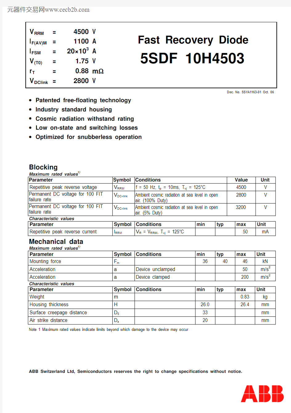

V RRM= 4500 V I F(AV)M= 1100 A I FSM= 20×103A V(T0)= 1.75 V r T= 0.88 m?V DClink= 2800 V Fast Recovery Diode
5SDF 10H4503
Doc. No. 5SYA1163-01 Oct. 06
?Patented free-floating technology
?Industry standard housing
?Cosmic radiation withstand rating
?Low on-state and switching losses
?Optimized for snubberless operation
Blocking
Maximum rated values 1)
Parameter Symbol Conditions Value Unit Repetitive peak reverse voltage V RRM f = 50 Hz, t p = 10ms, T vj = 125°C 4500 V
Permanent DC voltage for 100 FIT failure rate V DC-link Ambient cosmic radiation at sea level in open
air. (100% Duty)
2800 V
Permanent DC voltage for 100 FIT failure rate V DC-link Ambient cosmic radiation at sea level in open
air. (5% Duty)
3200 V
Characteristic values
Parameter Symbol Conditions min typ max Unit Repetitive peak reverse current I RRM V R = V RRM, T vj = 125°C 50 mA Mechanical data
Maximum rated values 1)
Parameter Symbol Conditions min typ max Unit Mounting force F m 36 40 46 kN Acceleration a Device unclamped 50 m/s2 Acceleration a Device clamped 200 m/s2 Characteristic values
Parameter Symbol Conditions min typ max Unit Weight m0.83 kg Housing thickness H26.0 26.4 mm Surface creepage distance D S 33 mm Air strike distance D a 20 mm Note 1 Maximum rated values indicate limits beyond which damage to the device may occur
元器件交易网https://www.360docs.net/doc/7418875130.html,
ABB Switzerland Ltd, Semiconductors reserves the right to change specifications without notice.
On-state
Maximum rated values 1)
Parameter
Symbol Conditions min
typ max Unit Max. average on-state current
I F(AV)M
Half sine wave, T C = 70 °C 1100 A Max. RMS on-state current I F(RMS)
1740
A Max. peak non-repetitive surge current I FSM
20×103
A Limiting load integral I 2t t p = 10 ms, T vj = 125°C, V R = 0 V
2×10
6 A 2s Max. peak non-repetitive surge current I FSM
12×103
A Limiting load integral
I 2t
t p = 30 ms, T vj = 125°C, V R = 0 V
2.16×10⁶
A 2s Characteristic values
Parameter Symbol Conditions min typ max Unit On-state voltage V F I F = 2500 A, T vj = 125°C 3.1 3.8 V Threshold voltage V (T0) 1.75 V Slope resistance
r T
T vj = 125°C
I F = 500...2500 A
0.88
m ?
Turn-on
Characteristic values
Parameter
Symbol Conditions min
typ
max Unit dI F /dt = 600 A/μs, T vj = 125°C 80 V Peak forward recovery voltage
V FRM
dI F /dt = 3000 A/μs, T vj = 125°C
250
V
Turn-off
Maximum rated values 1)
Parameter
Symbol Conditions
min
typ
max Unit Max. decay rate of on-state current
di/dt crit I FM = 4000 A, T vj = 125 °C V DC-link = 2800 V
600
A/μs
Characteristic values
Parameter
Symbol Conditions min
typ
max Unit Reverse recovery current I RM 1520 A Reverse recovery charge Q rr 5250 μC Turn-off energy E rr
I FM = 3300 A, V DC-Link = 2800 V -dI F /dt = 600 A/μs, L CL = 300 nH C CL = 10 μF, R CL = 0.65 ?, T vj = 125°C, D CL = 5SDF 10H4503
9.5
J
Thermal
Maximum rated values
Note 1
Parameter Symbol Conditions min typ max Unit Operating junction temperature range
T vj
0 125 °C Storage temperature range T stg
-40 125 °C Characteristic values
Parameter
Symbol Conditions
min typ max Unit Thermal resistance junction to case R th(j-c) Double-side cooled F m = 36...46 kN 12 K/kW R th(j-c)A Anode-side cooled F m = 36...46 kN 24 K/kW
R th(j-c)C
Cathode-side cooled F m = 36...46 kN 24
K/kW Thermal resistance case to heatsink R th(c-h) Double-side cooled F m = 36...46 kN 3 K/kW
R th(c-h)
Single-side cooled F m = 36...46 kN
6
K/kW
Analytical function for transient thermal
impedance:
)
e -(1R = (t)Z n
1
i t/-i th c)-th(j ∑=i τ i 1 2 3 4 R th i (K/kW)
7.705 2.748 1.009 0.539
τi (s)
0.5244
0.0633
0.0065
0.0015
Fig. 1 Transient thermal impedance junction-to-case
Fig. 2 Max. on-state voltage characteristics
Fig. 3 Max. on-state voltage characteristics
Fig. 4 Surge on-state current vs. pulse length. Half-sine wave
Fig. 5 Surge on-state current vs. number of pulses,
half-sine wave, 10 ms, 50Hz
Fig. 6Upper scatter range of turn-off energy per pulse vs. turn-off current Fig. 7Upper scatter range of turn-off energy per pulse vs reverse current rise rate
Fig. 8Upper scatter range of repetitive reverse recovery charge vs reverse current rise rate.Fig. 9Upper scatter range of reverse recovery current vs reverse current rise rate
Fig. 10Diode Safe Operating Area
Fig. 11General current and voltage waveforms Array
Fig. 12Test circuit.
ABB Switzerland Ltd, Semiconductors reserves the right to change specifications without notice.
ABB Switzerland Ltd Doc. No. 5SYA1163-01 Oct. 06
Semiconductors Fabrikstrasse 3
CH-5600 Lenzburg, Switzerland
Telephone +41 (0)58 586 1419 Fax +41 (0)58 586 1306
Fig. 13 Outline drawing, all dimensions are in millimeters and represent nominal values unless stated otherwise
Related documents:
Doc. Nr Titel
5SYA 2036 Recommendations regarding mechanical clamping of Press Pack High Power Semiconductors
5SZK 9104 Specification of environmental class for pressure contact diodes, PCTs and GTO, STORAGE available on request, please contact factory
5SZK 9105
Specification of environmental class for pressure contact diodes, PCTs and GTO, TRANSPORTATION available on request, please contact factory
Please refer to https://www.360docs.net/doc/7418875130.html,/semiconductors for actual versions.