MSA-0311中文资料

Cascadable Silicon Bipolar MMIC?Amplifier Technical Data
Features
?Cascadable 50 ? Gain Block ? 3 dB Bandwidth:DC to 2.3 GHz ?11.0 dB Typical Gain at 1.0?GHz ?9.0 dBm Typical P 1 dB at --1.0?GHz ?Unconditionally Stable (k>1)?Low Cost Surface Mount Plastic Package ?Tape-and-Reel Packaging Option Available [1]
MSA-0311
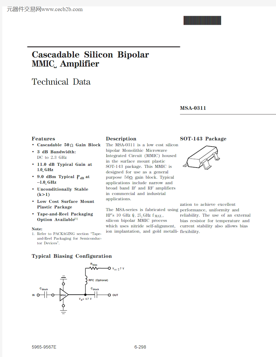
SOT-143 Package
Description
The MSA-0311 is a low cost silicon bipolar Monolithic Microwave Integrated Circuit (MMIC) housed in the surface mount plastic SOT-143 package. This MMIC is designed for use as a general purpose 50 ? gain block. Typical applications include narrow and broad band IF and RF amplifiers in commercial and industrial applications.
The MSA-series is fabricated using HP’s 10 GHz f T , 25?GHz f MAX ,silicon bipolar MMIC process which uses nitride self-alignment,ion implantation, and gold metalli-
Typical Biasing Configuration
R
V CC > 7 V
IN
OUT
Note:
1.Refer to PACKAGING section “Tape-and-Reel Packaging for Semiconduc-tor Devices”.
zation to achieve excellent performance, uniformity and reliability. The use of an external bias resistor for temperature and current stability also allows bias flexibility.
MSA-0311 Absolute Maximum Ratings
Parameter
Absolute Maximum [1]
Device Current
60 mA Power Dissipation [2,3]240 mW RF Input Power
+13 dBm Junction Temperature 150°C Storage Temperature
–65 to 150°C
Thermal Resistance [2,4]:
θjc = 500°C/W
Notes:
1.Permanent damage may occur if any of these limits are exceeded.
2.T CASE = 25°C.
3.Derate at 2.0 mW/°C for T C > 30°C.
4.See MEASUREMENTS section “Thermal Resistance” for more information.
Part Number Ordering Information
Part Number No. of Devices
Container MSA-0311-TR130007" Reel MSA-0311-BLK
100
Antistatic Bag
For more information, see “Tape and Reel Packaging for Semiconductor Devices”.
Electrical Specifications [1], T A = 25°C
Symbol
Parameters and Test Conditions: I d = 35 mA, Z O = 50 ?
Units
Min.
Typ.
Max.
G P Power Gain (|S 21|2) f = 0.1 GHz dB
11.5f = 1.0 GHz 9.0
11.0?G P Gain Flatness f = 0.1 to 1.6 GHz
dB ±0.7f 3 dB 3 dB Bandwidth GHz
2.3I nput VSWR f = 0.1 to
3.0 GHz 1.5:1Output VSWR f = 0.1 to 3.0 GHz 1.7:1
NF 50 ? Noise Figure
f = 1.0 GHz dB 6.0P 1 dB Output Power at 1 dB Gain Compression f = 1.0 GHz dBm 9.0IP 3Third Order Intercept Point f = 1.0 GHz dBm 22.0t D Group Delay f = 1.0 GHz psec 140V d Device Voltage
T C = 25°C V 3.8
4.7
5.6
dV/dT
Device Voltage Temperature Coefficient
mV/°C
–8.0
Notes:
1.The recommended operating current range for this device is 20 to 40 mA. Typical gain performance as a function of current is on the following page.
VSWR
Typical Performance, T A = 25°C
(unless otherwise noted)
G p (d B )
FREQUENCY (GHz)
Figure 1. Typical Power Gain vs. Frequency, I d = 35 mA.
2468
10
1214I d (mA)
Figure 2. Power Gain vs. Current.
4
6
8
10
12
14
G p (d B )
15
25
3040
50
35
20
N F (d B )
FREQUENCY (GHz)
Figure 4. Noise Figure vs. Frequency, I
d = 35 mA.
0.1
0.20.3
0.5
2.0
1.0
4.0
0.1
0.20.30.5 2.0
1.0FREQUENCY (GHz)
Figure 3. Output Power at 1 dB Gain Compression vs. Frequency, I d = 35 mA.
036
9121518P 1 d B (d B m )
MSA-0311 Typical Scattering Parameters (Z O = 50 ?, T A = 25°C, I d = 35 mA)
Freq.GHz
Mag
Ang
dB
Mag
Ang
dB
Mag
Ang
Mag
Ang
0.1.062511.7 3.84175–17.9.1272.24–70.2.073111.7 3.83170–17.9.1283.23–130.4.073811.6 3.78159–17.8.1296.24–280.6.073011.4 3.72149–17.6.13218.24–400.8.082111.2 3.65140–17.3.13611.24–531.0.081011.0 3.56130–17.0.14113.24–651.5.09–3210.4 3.31106–15.9.16017.24–912.0.09–1059.5 2.9984–14.9.17916.23–1152.5.13–1518.5 2.6670–14.1.19719.23–1333.0.19–1767.4 2.3551–13.5.21215.22–1453.5.24166 6.2 2.0435–13.0.22411.23–1514.0.27152 5.1 1.8020–12.7.2326.24–1515.0.36114 2.9 1.39–6–12.1.250–1.25–1526.0.50880.8 1.10–28–11.8.258–8.25–166
A model for this device is available in the DEVICE MODELS section.
S 11S 21S 12 S 22
SOT-143 Package Dimensions
DIMENSIONS ARE IN MILLIMETERS (INCHES) Package marking code is “A03”