TBA820M-D08-T中文资料

UNISONIC TECHNOLOGIES CO.,
TBA820M LINEAR INTEGRATED CIRCUIT
1.2W AUDIO POWER AMPLIFIER
DESCRIPTION
The UTC TBA820M is a monolithic integrated audio amplifier. It is designed for audio frequency class b amplifier.
FEATURES
*Wide operating supply voltage: Vcc=3~14V *Medium output power
P OUT =1.2W at Vcc=9V,R L =8Ω, THD=10% *Low quiescent circuit current: I Q =4mA(type) *Good ripple rejection.
*Minimum number of external parts required.
*Pb-free plating product number: TBA820ML
ORDERING INFORMATION
Order Number
Normal Lead Free Plating
Package Packing
TBA820M-S08-R TBA820ML-S08-R SOP-8 Tape Reel TBA820M-S08-T TBA820ML-S08-T SOP-8 Tube
TBA820M-D08-T TBA820ML-D08-T DIP-8 Tube
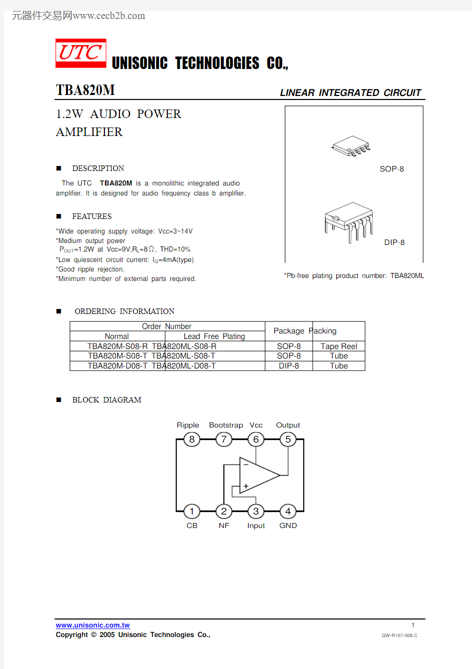
BLOCK DIAGRAM
Ripple Bootstrap Vcc Output
CB
NF
Input
GND
ABSOLUTE MAXIMUM RATINGS (T a =25°C)
PARAMETER SYMBOL RATINGS UNIT
Supply Voltage Vcc 16 V Output Peak Current I O(peak) 1.5 A Power Dissipation P D 1.25 W Operating Temperature T OPR 0 ~ +70 °C Storage Temperature T STG -40 ~ +150 °C
Note:1. Absolute maximum ratings are stress ratings only and functional device operation is not implied. The device
could be damaged beyond Absolute maximum ratings.
2. The device is guaranteed to meet performance specifications within 0℃~70℃ operating temperature range and assured by design from –20℃~85℃.
ELECTRICAL CHARACTERISTICS
(T a =25°C, V cc =9V, F=1KHZ, R G =600?, R F =120?, R L =8?, unless otherwise specified.
PARAMETER SYMBOL TEST CONDITIONS MIN TYP MAX UNIT
Quiescent Current I Q V IN =0 4 12 mA
Vcc=9V,R L =4?,THD=10% 1.6 Vcc=9V,R L =8?,THD=10% 0.9 1.2
Vcc=6V,R L =4?,THD=10% 0.75
Vcc=6V,R L =8?,THD=10% 0.4 0.5 Output Power P OUT Vcc=12V,R L =8?,THD=10% 2
W Total Harmonic Distortion THD P OUT =500mW 0.3 1 % Open Loop Voltage Gain Gvo R F =0 75 dB Closed Loop Voltage Gain Gvc R F =120? 33 36 39 dB Input Resistance R IN 5 M ? Output Noise Voltage eN R G =10k ?, BW(-3dB)=50~20kHz 0.3 1 mV
TEST CIRCUIT
V CC
TYPICAL CHARACTERISTICS
Fig 1 Quienscent circuit current vs
Supply Voltage Fig 2 Output power vs Supply Voltage
04
8
Q u i e s c e n t C u r r e n t (m A )
T o t a l h a r m o n i c D i s t o r t i o n ( %)
048
12160
0.4
0.8
1.2
1.6
Output Power(W) 2.0
P o w e r D i s s i p a t i o n (W )
4
8
12
16
Supply Voltage (V)
20
TYPICAL CHARACTERISTICS(CONT.)
Fig 7 Frequency response
Fig 8 Total Harmonic distortion vs frequency
10
10
310
210410
510
10
3
10
2
10410
50Frequency(Hz)
Frequency(Hz) R e s p o n s e (d B )
-5
-3-1
13