nnano.2014.186
664 NATURE NANOTECHNOLOGY | VOL 9 | SEPTEMBER 2014 | https://www.360docs.net/doc/8b18877854.html,/naturenanotechnology news & views
independently, for example by applying a voltage on a gate electrode. The method used by Nitta and colleagues gives precise information on the direction of the total spin–orbit field and, therefore, also of the α/β ratio.As well as introducing a new intriguing concept in the physics of interference transport phenomena, the method has practical implications for the research of spintronic devices. Spin-transistor structures, in which electrical control of on and off states is achieved using the spin of the electrons flowing in the transistor channel 4–6, rely on coherent precession of spins of carriers injected into the channel. When α/β = 1, the spin–orbit-field axis becomes independent of momentum, and confining the electrons to the narrow quasi-1D channel is not required to preserve spin coherence 7. The method developed by Nitta and colleagues allows this optimal spin–orbit-coupling field to be found and to be used to manipulate spins without destroying the spin information. ?Tomas Jungwirth and J?rg Wunderlich are at the Institute of Physics ASCR, v.v.i., Cukrovarnicka 10,
162 53 Praha 6, Czech Republic. Tomas Jungwirth is also at the School of Physics and Astronomy, University of Nottingham, Nottingham NG7 2RD, UK. J?rg Wunderlich is also at the Hitachi Cambridge Laboratory, Cambridge CB3 0HE, UK. e-mail: jw526@https://www.360docs.net/doc/8b18877854.html, References 1. Bergmann, G. Solid State Commun . 42, 815–817 (1982).2. Sasaki, A. et al. Nature Nanotech . 9, 703–709 (2014).3. Scheid, M., Kohda, M., Kunihashi, Y., Richter, K. & Nitta, J. Phys. Rev. Lett. 101, 266401 (2008).4. Datta, S. & Das, B. Appl. Phys. Lett . 56, 665–667 (1990).5. Koo, H. C. et al. Science 325, 1515–1518 (2009).6. Wunderlich, J. et al. Science 330, 1801–1804 (2010).7. Bernevig, B. A., Orenstein, J. & Zhang, S.-C. Phys. Rev. Lett .
97, 236601 (2006).
TWO-DIMENSIONAL MATERIALS Atomically thin p–n junctions Van der Waals heterostructures consisting of a single MoS 2 monolayer and a single WSe 2 monolayer can be used to form p–n junctions.
Su-Fei Shi and Feng Wang A p–n junction is formed at the boundary between a hole-doped (p-type) and electron-doped (n-type) semiconductor, and creates an electrical field due to electron transfer from the n-type region to the p-type region. This built-in electrical field leads to diode behaviour, which is characterized by asymmetric charge transport under forward and backward biases. Such semiconductor diodes are ubiquitous in modern electronics and optoelectronics, ranging from rectifying diodes, frequency
mixing diodes and tunnelling diodes to photodiodes, light-emitting diodes and laser diodes. A key parameter in semiconductor diodes is the thickness of the p–n junction, which is typically 10 nm to 1 μm depending on the diode type. Atomically thin layers of two-dimensional (2D) semiconductors, such as transition metal dichalcogenides, offer opportunities for engineering novel semiconductor p–n junctions. Writing in Nature Nanotechnology , Philip Kim and co-workers at Columbia University,
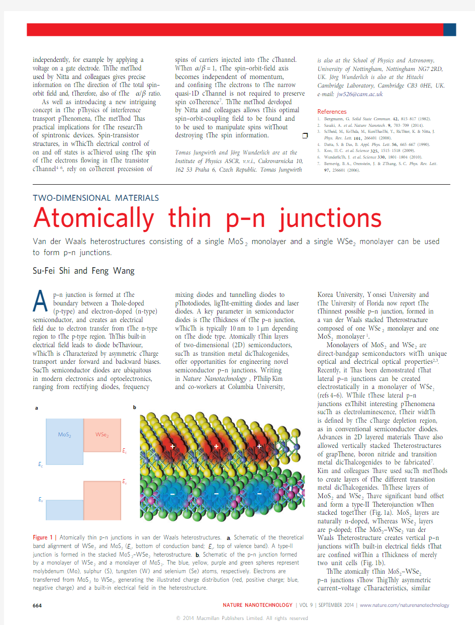
Korea University, Y onsei University and the University of Florida now report the thinnest possible p–n junction, formed in a van der Waals stacked heterostructure composed of one WSe 2 monolayer and one MoS 2 monolayer 1.Monolayers of MoS 2 and WSe 2 are direct-bandgap semiconductors with unique optical and electrical optical properties 2,3. Recently, it has been demonstrated that lateral p–n junctions can be created electrostatically in a monolayer of WSe 2 (refs 4–6). While these lateral p–n junctions exhibit interesting phenomena such as electroluminescence, their width is defined by the charge depletion region, as in conventional semiconductor diodes. Advances in 2D layered materials have also allowed vertically stacked heterostructures of graphene, boron nitride and transition metal dichalcogenides to be fabricated 7. Kim and colleagues have used such methods to create layers of the different transition metal dichalcogenides. These layers of MoS 2 and WSe 2 have significant band offset and form a type-II heterojunction when stacked together (Fig. 1a). MoS 2 layers are naturally n-doped, whereas WSe 2 layers are p-doped; the MoS 2–WSe 2 van der Waals heterostructure creates vertical p–n junctions with built-in electrical fields that are confined within a thickness of merely two unit cells (Fig. 1b).The atomically thin MoS 2–WSe 2 p–n junctions show highly asymmetric
current–voltage characteristics, similar MoS 2
WSe 2
E
c E v E c E v
a b Figure 1 | Atomically thin p–n junctions in van der Waals heterostructures. a , Schematic of the theoretical
band alignment of WSe 2 and MoS 2 (E c , bottom of conduction band; E v , top of valence band). A type-II
junction is formed in the stacked MoS 2–WSe 2 heterostructure. b , Schematic of the p–n junction formed
by a monolayer of WSe 2 and a monolayer of MoS 2. The blue, yellow, purple and green spheres represent
molybdenum (Mo), sulphur (S), tungsten (W) and selenium (Se) atoms, respectively. Electrons are
transferred from MoS 2 to WSe 2, generating the illustrated charge distribution (red, positive charge; blue,
negative charge) and a built-in electrical field in the heterostructure.
? 2014 Macmillan Publishers Limited. All rights reserved
NATURE NANOTECHNOLOGY | VOL 9 | SEPTEMBER 2014 | https://www.360docs.net/doc/8b18877854.html,/naturenanotechnology
665news & views to conventional semiconductor diodes. The microscopic origin of this electrical rectification behaviour, however, is rather different. In conventional semiconductor diodes, a depletion region exists across the thickness of p–n junctions, and semi-classical drift and diffusion of charge carriers through the depletion region often controls the electrical rectification. In contrast, quantum tunnelling of electrons becomes increasingly important when the thickness of the p–n junction is decreased, and Kim and colleagues show that quantum tunnelling dominates charge transport across the atomically thin p–n junctions.The vertical MoS 2–WSe 2 p–n junctions also exhibit interesting optoelectronic responses. Using spatially resolved photocurrent measurements, the researchers observed a strong photocurrent generated at the WSe 2–MoS 2 heterojunction, indicating efficient separation of photoexcited electrons and holes. This electron–hole separation also leads to strongly quenched fluorescence in the heterostructure compared with that of bare WSe 2 or MoS 2. The photocurrent
generated in MoS 2–WSe 2 p–n junctions depends sensitively on the interlayer recombination rate of layer-separated electrons and holes, which can be controlled through electrostatic gating. The maximum photocurrent is reached when a minimum interlayer electron–hole recombination rate is achieved by gating. Furthermore, Kim and colleagues show that sandwiching the atomic p–n junction between graphene layers could enhance the collection of the photoexcited carriers by eliminating the slow charge diffusion along the rather resistive transition metal dichalcogenides.
Two other independent research teams, led by Thomas Mueller and Xiangfeng Duan, have also recently reported the generation of photocurrent in similar heterostructures composed of stacked 2D MoS
2 and WSe 2 layers 8,9; electroluminescence was, in addition, observed in these atomically thin vertical p–n junctions 9
. The interesting electrical and optoelectronic behaviour reported in all three of these studies illustrates the exciting opportunities offered by van der Waals heterostructures, which can be composed of a rich variety of 2D crystals 7.
These van der Waals heterostructures also generate many new questions about their underlying physics. Take, for example, the charge transfer and photocurrent generation in the MoS 2–WSe 2 p–n junctions. What is the dynamic evolution governing the charge transfer process? Do the layer-separated electrons and holes form exciton states given the strong Coulomb interactions in 2D? Can the band alignment of MoS 2 and WSe 2 be controlled by electrostatic gating? Further exploration of the atomically thin p–n junctions, and van der Waals heterostructures more generally, will advance our understanding of 2D physics and lead to new technological developments. ?Su-Fei Shi and Feng Wang are in the Department of Physics, University of California, 366 LeConte Hall #7300, Berkeley, California 94720-7300, USA. e-mail: fengwang76@https://www.360docs.net/doc/8b18877854.html, References 1. Lee, C-H. et al. Nature Nanotech. 9, 676–681 (2014).2. Splendiani, A. et al. Nano Lett. 10, 1271–1275 (2010).3. Mak, K. F., Lee, C., Hone, J., Shan, J. & Heinz, T. F. Phys. Rev. Lett. 105, 136805 (2010).4. Baugher, B. W . H., Churchill, H. O. H., Yang, Y. & Jarillo-Herrero, P . Nature Nanotech. 9, 262–267 (2014).5. Ross, J. S. et al. Nature Nanotech. 9, 268–272 (2014).6. Pospischil, A., Furchi, M. M. & Mueller, T. Nature Nanotech. 9, 257–261 (2014).7. Geim, A. K. & Grigorieva, I. V . Nature 499, 419–425 (2013).8. Furchi, M. M., Pospischil, A., Libisch, F., Burgd?rfer, J. & Mueller, T. Preprint at https://www.360docs.net/doc/8b18877854.html,/abs/1403.2652 (2014).9. Cheng, R. et al. Preprint at https://www.360docs.net/doc/8b18877854.html,/abs/1403.3447 (2014).? 2014 Macmillan Publishers Limited. All rights reserved